Introduction
Multijunction solar cells combine multiple semiconducting materials into a single device to achieve efficiencies well beyond what is possible with traditional single-junction devices. While single-junction GaAs solar cells have achieved solar-to-electric conversion efficiencies of 29%, efficiencies up to 46% have already been demonstrated using four-junction devices under concentrated sunlight illumination.Reference France, Geisz, Garcia, Steiner, McMahon, Friedman, Moriarty, Osterwald, Ward, Duda, Young and Olavarria1,Reference Dimroth, Tibbits, Niemeyer, Predan, Beutel, Karcher, Oliva, Siefer, Lackner, Bett, Krause, Drazek, Guiot, Wasselin, Tauzin and Signamarcheix2 Currently, multijunction cells are primarily used by the space industry for power generation on satellites or spacecraft, where the high efficiency lowers the required weight of the solar array for a given power. These cells are also used for terrestrial power generation in concentrator photovoltaic systems, where the amount of solar cell material is reduced by the concentration factor (the ratio of illuminated area to cell area), and the concentration improves device efficiency due to a logarithmic increase in the voltage with light intensity. The performance increase under concentrated light, combined with the natural high performance of multijunction solar cells, has led to the highest reported photovoltaic efficiencies of any technology.Reference Green, Emery, Hishikawa, Warta and Dunlop3
While many multijunction solar cell designs exist, such as wafer-bondedReference Dimroth, Tibbits, Niemeyer, Predan, Beutel, Karcher, Oliva, Siefer, Lackner, Bett, Krause, Drazek, Guiot, Wasselin, Tauzin and Signamarcheix2 or printed approaches,Reference Sheng, Bower, Bonafede, Wilson, Fisher, Meitl, Yuen, Wang, Shen, Banks, Corcoran, Nuzzo, Burroughts and Rogers4 this article focuses on metamorphic multijunction solar cells. Metamorphic epitaxy provides access to a wide selection of III–V compounds as potential absorber materials, enabling an optimal bandgap combination within a multijunction solar cell. However, metamorphic solar cells contain dislocations that can significantly reduce the solar cell performance if their density is not carefully controlled. We discuss the benefits and drawbacks of metamorphic materials for photovoltaic applications, describe the materials science of metamorphic buffers for multijunction solar cells, and demonstrate the designs and performance of different metamorphic multijunction approaches.
Background
Motivation for metamorphic multijunction solar cells
The efficiency advantage of multijunction solar cells over single-junction solar cells is the reduction of losses due to carrier thermalization and photon transmission.Reference Friedman5–Reference Philipps, Guter, Welser, Schone, Steiner, Bett, Lopez, Vega and Luque8 An incoming photon with energy above the semiconductor bandgap (i.e., hν ≥ E g, where h is Planck’s constant, ν is the photon frequency, and E g is the bandgap energy) is absorbed and generates an electron–hole pair that may contribute to the device current. The excess energy of the photon above the bandgap is lost as heat as the photogenerated electron–hole pair quickly thermalizes to the semiconductor band edge, and photons with energy less than the bandgap are not absorbed. In a properly designed multijunction device, each subcell receives a portion of the solar spectrum with energy only slightly greater than its bandgap, thereby reducing the total thermalization loss and improving the efficiency. Additionally, the bandgaps of the subcells are chosen to span most of the wavelength range of the solar spectrum, that ranges from 300 nanometers to several micrometers, and therefore reduce losses due to transmission of photons. This combination of low thermalization and transmission loss has so far only been achieved in multijunction solar cell devices.
High material quality—meaning a low internal defect concentration—is necessary for the highest photovoltaic performance. Defects often introduce electronic states within the bandgap of the host semiconductor, where these states act as nonradiative recombination centers for photogenerated electron–hole pairs. Single-crystal III–V and Group IV semiconductors such as GaInP, GaAs, and Ge are commonly employed as absorber materials because they can be produced with very high material quality, are easily doped (both n- and p-type), and possess alloy compositions with a wide range of bandgaps.
For a given number of junctions in a multijunction device, the operating conditions of spectrum, temperature, and concentration determine the optimal bandgap combination. However, combining alloys with optimal bandgaps is a challenge, in part, because the most desirable materials have different lattice constants, and the selection of high-quality single-crystal growth substrates is limited. Figure 1a shows the available standard III–V and Group IV alloys, with the optimal bandgap combination for two-, three-, and four-junction devices indicated as determined previously,Reference Friedman5,Reference France, Geisz, Steiner, Friedman, Ward, Olson, Olavarria, Young and Duda9 using the 500× concentrated direct spectrum and assuming near-perfect material quality. Any combination of (non-nitride) III–V materials with the optimal direct bandgaps involves lattice mismatch between the materials or to elemental or binary semiconductor growth substrates. Thus, lattice-matched epitaxy of standard III–V materials cannot produce multijunction solar cells with an optimal bandgap combination.
(a) Bandgaps and lattice constants of high-quality III–V ternaries and SiGe binaries used in multijunction solar cells, and the approximate optimal bandgaps for two,- three,- and four-junction devices (2J, 3J, and 4J, respectively). The modelReference Friedman5,Reference France, Geisz, Steiner, Friedman, Ward, Olson, Olavarria, Young and Duda9 uses the 500× concentrated direct terrestrial spectrum (AM1.5D) with the device at 25°C. The ideal bandgaps for a multijunction device cannot be achieved using standard semiconductors with the same lattice constant. The black tie lines indicate potential metamorphic materials that can be used to optimize device bandgaps. (b) Modeled efficiency of a two-junction solar cell as a function of its bandgaps, assuming near-perfect material quality. GaInP/GaAs is not the optimal bandgap combination, but in practice, is the highest efficiency two-junction cell because of its high crystal quality. Metamorphic multijunction cells need to have extremely high quality (low dislocation density) in order to benefit from having the ideal bandgap combination.

Metamorphic epitaxy enables an optimal bandgap combination by combining alloys with different lattice constants, and thus has the potential for the highest possible multijunction solar cell efficiency. However, lattice-mismatched materials have dislocations that can significantly lower performance by increasing nonradiative recombination. In addition, very high efficiency can still be achieved by using lattice-matched compounds that have near-perfect material quality, but a nonoptimal bandgap combination. Figure 1b shows the modeled efficiency of a two-junction device, under the 500× concentrated direct spectrum, as a function of its bandgaps.Reference Friedman5,Reference France, Geisz, Steiner, Friedman, Ward, Olson, Olavarria, Young and Duda9 While not the optimal bandgap combination, the highest performing two-junction device currently is 1.8-eV Ga0.5In0.5P/1.4-eV GaAs,Reference Steiner, Geisz, Garcia, Friedman, Duda, Olavarria, Young, Kuciauskas and Kurtz10 because the junctions are lattice-matched to a high-quality GaAs substrate and are themselves very high quality. Likewise, the current multijunction cell most commonly used by the space industry is an all lattice-matched monolithic GaInP/GaInAs/Ge device grown on a germanium substrate.Reference Fetzer, Jun, Edmonds, Khemthong, Rouhani, Cravens, Bardfield and Gillanders11 Careful control of the metamorphic epitaxy is required such that the efficiency gains from the optimal bandgap combination outweigh the losses.
Dislocations and solar cell performance
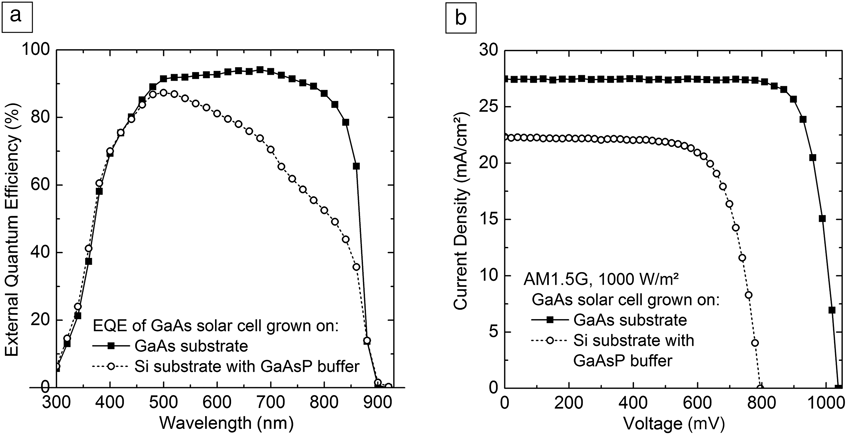
Research into metamorphic III–V solar cells has been ongoing for over 30 years due to the potential for high-efficiency solar cells on low-cost substrates. Initially, GaAs solar cells were directly grown on Si substrates, which resulted in a high density of dislocations due to the 4% lattice mismatch. The dislocations were found to act as minority-carrier recombination centers and significantly lowered the minority-carrier diffusion length and device performance when the spacing between dislocations was shorter than the diffusion length in nondislocated material, experimentally demonstrated in Figure 2.
Losses from dislocations are experimentally observed by comparing lattice-matched GaAs solar cells with lattice-mismatched GaAs-on-Si solar cells with about 108 cm–2 dislocation density,Reference Roesener12 using (a) external quantum efficiency (EQE) and (b) standard illuminated current density–voltage (J–V) curves, measured under the terrestrial global (AM1.5G) spectrum. High dislocation density reduces the EQE, thus the current, and lowers the voltage of the device.
Yamaguchi and others modeled the relationship between the dislocation density and solar cell properties and predicted that dislocation densities below 106 cm–2 are necessary to limit nonradiative loss in metamorphic solar cells.Reference Yamaguchi and Amano13,Reference Andre, Wilt, Pitera, Lee, Fitzgerald and Ringel14 The dislocation density is thus a principal metric for lattice-mismatched solar cells and can be measured using a variety of strain-sensitive or recombination-based imaging techniques.Reference Fitzgerald15 Direct deposition of GaAs on Si, even when using multistep nucleation methods, results in dislocation densities of 108–109 cm–2. Methods to reduce the dislocation density, such as thermal cycling, selective area growth, and strained-layer superlattices, were shown to lower the dislocation density in these devices to around 107 cm–2, but not to the level necessary for high-quality solar cells.Reference Ringel, Grassman and Li16
Materials science for metamorphic solar cells
Despite the fact that high dislocation densities are detrimental to photovoltaic performance, it is important to recognize that metamorphic solar materials actually require them in order to relieve lattice-mismatch strain energy. This section provides a brief introduction to metamorphic epitaxy for solar cells, and more detailed references on dislocation fundamentals and strained-layer epitaxy can be found elsewhere.Reference Fitzgerald15,Reference Hull and Bacon17–Reference Beanland, Dunstan and Goodhew20
Graded buffers for metamorphic solar cells
The subcells of a III–V multijunction solar cell are typically 1–3 μm thick in order to fully absorb the incoming solar spectrum. At this thickness, even a small lattice mismatch results in enough elastic energy to surpass activation energies for dislocation nucleation and glide. The epitaxial thickness at which dislocation glide is energetically favorable for a given strain is called the “critical thickness,” and has been modeled by many researchers.Reference Fitzgerald15,Reference Matthews and Blakeslee21,Reference People and Bean22 Other optoelectronic devices can access useful bandgaps without the formation of dislocations by utilizing thin, strained layers that remain below the critical thickness, but solar cells cannot due to their requirement for thick absorbers. For solar cells, controlled formation of strain-relieving dislocations is necessary such that the subsequent thick absorber material can be grown without strain, making it stable against plastic relaxation.
The strain relief provided by misfit dislocations is accomplished through the introduction/subtraction of extra/excess crystal planes, and the “misfit dislocation loop” is the crystallographic boundary that surrounds and defines each extra/missing plane. Relief of this strain moves the in-plane lattice constant away from that of the underlying substrate and toward the equilibrium lattice constant of the epitaxial material, allowing subsequent growth of thick and strain-free lattice-mismatched material. The associated dislocation loops are made up of two main parts (illustrated in Figure 3): misfit segments, which lie on the horizontal plane of the mismatched interface and provide the majority of the strain relief; and threading segments, which extend semi-vertically to the sample surface and are largely responsible for device performance loss.
(a) Illustration and (b) cross-sectional transmission electron microscope (TEM) image of a compositionally graded buffer within a multijunction solar cell. The lattice constant (a R) is slowly increased throughout the buffer, which gradually increases strain. Dislocations (green lines in illustration, and sharp contrast lines in TEM) form and glide to relieve the strain, allowing a strain-free, lattice-mismatched subcell with a low threading dislocation density (TDD) to be grown. (c) Plan-view 100 μm × 100 μm electron-beam-induced current image, measuring a TDD below 106 cm–2 in the active region of a metamorphic Ga0.7In0.3As solar cell.
Compositionally graded buffers (see Figure 3) provide a route to controlled formation of dislocations while confining the majority of dislocation line length within the inactive buffer material.Reference Fitzgerald15,Reference Dodson and Tsao19,Reference Beanland, Dunstan and Goodhew20 The graded buffer consists of a sequence of layers slowly increasing in lattice-mismatch (strain) with respect to the initial substrate, which gradually increases the elastic energy. At the low levels of strain present in graded buffers, a limited number of “glissile” or mobile dislocations form and relieve strain through the glide of the threading segments that increases the length of the misfit segment. Promoting long glide of such dislocations maximizes their individual strain-relief efficacy and minimizes the total number needed to relieve a set amount of strain. Although unrealistic, the threading dislocations would ideally glide to the wafer edges and leave only the misfit segments within the inactive graded buffer, relieving strain without leaving threading dislocations in the photoactive material. Long misfit segments can also be formed via annihilation reactions between dislocations gliding on the same plane.
The slowly increasing strain energy throughout the compositionally graded buffer serves as the driving force acting upon the mobile dislocations, encouraging glide. The average glide length 〈l〉 of a dislocation is related to the linear misfit dislocation density (ρm, units of dislocations/cm) and areal threading dislocation density (TDD, ρt, units of dislocations/cm2) as 〈l〉 = 4 ρm/ρt, where the factor of four is due to the two threading arms per misfit dislocation and the two dimensions of strain relief. The strain relief (Δε) is related to the misfit dislocation density by the parallel edge component of the Burgers vector, b ||, as  $\Delta \varepsilon = \rho _m b_\parallel $, and the relaxed lattice constants on either side of the buffer (a 1 and a 2) as:
 $\Delta \varepsilon = {\raise0.7ex\hbox{${a_1 }$} \!\mathord{\left/ {\vphantom {{a_1 } {a_2 }}}\right.\kern-\nulldelimiterspace}\!\lower0.7ex\hbox{${a_2 }$}} - 1$. Rearranging these equations gives:
 $$\rho _t = {{4\Delta \varepsilon } \over { - \langle l\rangle b_{||} }}.$$
Thus, maximizing 〈l〉 gives the minimum residual TDD for a given strain relief (i.e., for a given change in relaxed lattice constant). This is the goal of a compositionally graded buffer, achieved by the gradual increase of low levels of strain.
Dislocation glide and microstructure influence
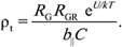
The dynamics of strain relaxation and dislocation glide were modeled kinetically by Dodson and TsaoReference Dodson and Tsao23 and later expanded by Fitzgerald et al.Reference Fitzgerald, Kim, Currie, Langdo, Taraschi and Bulsara24,Reference Fitzgerald, Xie, Monroe, Silverman, Kuo, Kortan, Thiel and Weir25 to describe the residual TDD (ρt) in an ideal graded buffer. The TDD depends on intrinsic material properties, the buffer structure, and growth conditions:
 $\rho _t = {{R_G R_{GR} e^{U/kT} } \over {b_{||} C}}.$
The glide velocity ( $v = Ce^{ - U/kT} $) is dependent on material constants (C), temperature (T), and activation energy for glide (U), and has been measured for many semiconductor materials.Reference Yonenaga26 The elastic properties of the material and solid-solution hardening play a strong role and vary as a function of composition.Reference Klinger, Roesener, Lorenz, Petzold and Dimroth27 Materials with low glide velocities, such as GaP, tend to result in higher ρt compared to high-glide velocity materials, such as InP. Low growth rate (R G), low misfit grade rate (R GR, % strain per thickness), and increased growth temperature all encourage glide and thus reduce the residual ρt. However, only a certain range of growth conditions are realistically possible due to practical limitations on deposition and growth temperatures that limit the achievable ρt. In addition, these models are fairly simplistic and ignore interactions between dislocations and other internal material properties.
Material microstructure such as compositional fluctuations, surface roughness, existing dislocations, precipitates, or other internal defects, also heavily influence dislocation nucleation and glide. The influence of these phenomena on dislocation glide depends on the materials system in the graded buffer. For instance, gliding threading segments can interact with each other as well as the underlying misfit segments.Reference Freund28,Reference Schwarz29 Crosshatch roughness, shown in Figure 4a, typically develops during metamorphic growth and can lead to significant overlap between the crosshatch troughs and the strain fields of underlying misfit dislocations when the roughness is excessive. Gliding dislocations can be pinned at the troughs, forcing the nucleation of new dislocation loops to continue strain relaxation, a phenomenon shown to significantly influence the glide and residual TDD of SixGe1–x buffers.Reference Samavedam and Fitzgerald30,Reference Currie, Samavedam, Langdo, Leitz and Fitzgerald31
Three material microstructures that influence glide. (a) Atomic force microscope image of metamorphic GaInP showing typical crosshatch roughness that can increase pinning dislocation interactions under the valleys. The image scale bar is on the right of the image, and the height of a line scan (blue line) is shown on the bottom of the image. (b) Transmission electron microscope image of phase separation in a GaxIn1–xP graded buffer, showing large pileups of pinned dislocations. Reprinted with permission from Reference Reference Quitoriano and Fitzgerald32. © 2007 American Institute of Physics. (c) Illustration showing how dislocations (green) in atomically ordered Ga0.5In0.5P disrupt the order pattern, which is energetically favorable.Reference France, McMahon, Norman, Geisz and Romero34
An issue in some graded III–V buffers is the presence of a solid-solution miscibility gap, which can lead to phase separation within the buffer and an associated variable internal strain field. Dislocations gliding through the phase-separated material thus receive a variable stress and are pinned at locations with low stress. GaxIn1–xP- and GaxIn1–xAs-based buffers with high indium content have been shown to readily phase separate;Reference Fitzgerald, Kim, Currie, Langdo, Taraschi and Bulsara24,Reference Quitoriano and Fitzgerald32 this drastically increases the dislocation density, as shown by the transmission electron microscope image in Figure 4b.
Atomic ordering in III–V materials has been shown to enhance glide.Reference McMahon, Kang, France, Norman, Friedman and Wei33 Ordered III–V materials are generally metastable, and dislocations that glide through ordered planes release stored energy by disrupting the order pattern (see Figure 4c). While this is potentially beneficial for dislocation dynamics, it has also been observed that dislocations can form when transitioning between ordered and disordered GaInP,Reference France, McMahon, Norman, Geisz and Romero34 thereby requiring careful control of growth conditions and buffer design.Reference France, Garcia, McMahon, Norman, Simon, Geisz, Friedman and Romero35
Residual strain accommodation
Residual strain in the photoactive carrier-collecting regions of the subcells provides a driving force for dislocation glide that could lead to misfit dislocations in the photoactive region and substantial nonradiative recombination. To ensure that the solar cell structure is strain free, the relaxed lattice constant of the solar cell structure has to be matched to the in-plane lattice constant of the last layer of the graded buffer, termed the “overshoot layer” (see Figure 3). The residual strain in the overshoot layer depends on many parameters, such as the TDD, buffer structure, material microstructure, and other parameters, so prior knowledge of this parameter is required in order to design strain-free subcells. Ex situ x-ray diffraction or in situ wafer curvature can be used to determine the residual strain of the overshoot layer and ensure strain-free growth of the subcell, thus avoiding the formation of long misfit segments within the photoactive material.
Metamorphic buffers resulting in low TDD
The epitaxy of metamorphic solar cells is challenging due to the complex interactions among epitaxial growth conditions, material properties, graded buffer structure, and dislocation dynamics. Nevertheless, understanding these interactions and controlling crosshatch roughness, phase separation, and atomic ordering has enabled high-quality solar cells to be demonstrated. In early work, Ringel et al. produced GaAs solar cells on Si substrates, a 4% lattice mismatch, using Si1–xGex graded buffers with a low TDD of ∼106 cm–2.Reference Sieg, Carlin, Boeckl, Ringel, Currie, Ting, Langdo, Taraschi, Fitzgerald and Keyes36,Reference Ringel, Carlin, Andre, Hudait, Gonzalez, Wilt, Clark, Jenkins, Scheiman, Allerman, Fitzgerald and Leitz37 Surface roughness, and its influence on the TDD in the SixGe1–x buffer, was controlled by chemomechanically polishing the metmorphic buffer at an intermediate stage: Si0.5Ge0.5.Reference Currie, Samavedam, Langdo, Leitz and Fitzgerald31 From Equation 1, a graded buffer with 106 cm–2 TDD and 4% strain relief requires ∼8 centimeter average dislocation glide length, demonstrating that graded buffers can effectively confine dislocations to inactive regions.
Since then, III–V graded buffers have been used to span lattice constants between GaAs and InP with dislocation densities of 106 cm–2 and lower by limiting any detrimental influence of atomic ordering or phase separation,Reference France, Geisz, Garcia, Steiner, McMahon, Friedman, Moriarty, Osterwald, Ward, Duda, Young and Olavarria1,Reference Quitoriano and Fitzgerald32,Reference France, Garcia, McMahon, Norman, Simon, Geisz, Friedman and Romero35,Reference Dimroth, Lanyi, Schubert and Bett38 allowing access to a wide range of available bandgaps. At these dislocation densities, the spacing between dislocations is on the same order as the minority carrier diffusion length, so performance loss is drastically reduced. The bandgap flexibility and high quality of the lattice-mismatched material is the basis for a diverse set of metamorphic multijunction designs, described next.
Metamorphic multijunction designs
Metamorphic epitaxy allows targeting semiconductor alloys with ideal bandgaps for the conversion of sunlight into electricity. The efficiency of these devices depends primarily on the material quality that can be obtained. However, commercial success depends heavily on factors, such as substrate cost, required thickness, and time for the growth of the solar cell device. These factors have led to a wide variety of metamorphic multijunction cell architectures and the development of metamorphic subcells with a large range of bandgaps. Here, we describe different approaches that have successfully led to high-efficiency multijunction devices (see Figure 5). The graded buffers and considerations are different for each approach. Because the graded buffer is often between two photoactive subcells, conductivity and transparency to the transmitted portion of the spectrum are required.
Illustrations of various high-efficiency metamorphic multijunction designs, where the active subcells are differently colored for clarity: (a) lattice-matched triple junction; (b) upright metamorphic; (c) inverted metamorphic; (d) multijunction on active Si; and (e) multijunction on inactive Si. Ge, GaAs, or Si substrates are used, and different bandgap combinations are targeted by using graded buffers.
Upright metamorphic multijunction
In the standard lattice-matched triple junction (Figure 5a), the Ge subcell receives excess photocurrent that is not utilized. The three-junction upright metamorphic (UMM) solar cell (Figure 5b) improves upon this design by lowering the bandgaps of the top two subcells through the use of a GaxIn1–xAs graded buffer grown on the Ge substrate, where the Ge substrate is still an active subcell.Reference King, Law, Edmonson, Fetzer, Kinsey, Yoon, Sherif and Karam39 The modified bandgap combination shown in the figure is 1.7-eV Ga0.35In0.65P/1.2-eV Ga0.83In0.17As/0.7-eV Ge, which more evenly distributes the incoming spectrum among the three subcells and raises the multijunction current.Reference Guter, Schöne, Philipps, Steiner, Siefer, Wekkeli, Welser, Oliva, Bett and Dimroth40 An upright metamorphic four-junction AlGaInP/AlGaInAs/GaInAs/Ge device has also been demonstrated.Reference Liu, Fetzer, Rehder, Cotal, Mesropian, Law and King41
The graded buffer of this UMM device typically needs to relieve 0.5–1.2% strain, for 1.3 to 1.2 eV GaInAs subcell bandgaps. This mismatch is relatively low, and dislocation densities below 106 cm–2 have been demonstrated for this device architecture, which has achieved over 41% efficiency under concentrated light.Reference Guter, Schöne, Philipps, Steiner, Siefer, Wekkeli, Welser, Oliva, Bett and Dimroth40,Reference King, Bhusari, Larrabee, Liu, Rehder, Edmonson, Cotal, Jones, Ermer, Fetzer, Law and Karam42 These GaxIn1–xAs graded buffers avoid the highly mixed ternary compositions where phase separation is an issue.Reference Quitoriano and Fitzgerald32 The buffer is also easily doped for conductivity and consists of compositions with wider bandgaps than the adjacent Ga0.83In0.17As subcell, making it naturally transparent to the filtered light that it receives.
Inverted metamorphic multijunction
In the inverted metamorphic (IMM) approach (Figure 5c),Reference Wanlass, Ahrenkiel, Ahrenkiel, Albin, Carapella, Duda, Geisz, Kurtz and Moriarty43 high-bandgap (Al)GaAs and/or (Al)GaInP subcells are grown first, lattice-matched and without dislocations, on a GaAs or Ge substrate. Graded buffers are then used to access low-bandgap lattice-mismatched GaInAs subcells. After growth, the device is removed from the substrate and inverted such that sunlight is incident on the highest bandgap subcell. Four-junction devices consisting of 1.8-eV Ga0.5In0.5P/1.4-eV GaAs/1.0-eV Ga0.7In0.3As/0.7-eV Ga0.45In0.55As with efficiency over 45% under concentrated light have been demonstrated,Reference France, Geisz, Garcia, Steiner, McMahon, Friedman, Moriarty, Osterwald, Ward, Duda, Young and Olavarria1 and structures with threeReference Geisz, Kurtz, Wanlass, Ward, Duda, Friedman, Olson, McMahon, Moriarty and Kiehl44,Reference Geisz, Friedman, Ward, Duda, Olavarria, Moriarty, Kiehl, Romero, Norman and Jones45 to six junctions have been reported.Reference Patel, Aiken, Chumney, Cornfeld, Lin, Mackos, McCarty, Miller, Sharps and Stan46
The metamorphic subcells of the IMM approach are highly mismatched, 1.0-eV GaInAs is 2% mismatched to GaAs and 0.7-eV GaInAs is 4% mismatched to GaAs, so the low-bandgap subcells require graded buffers with a wide lattice constant and composition range (Figure 1). In addition, the first graded buffer is below a GaAs subcell, so it needs to be transparent to light with a wavelength >870 nanometers (the GaAs bandgap). Graded GaxIn1–xAs would be absorbing, so wider-gap AlxGayIn1–x–yAs or GaxIn1–xP is used instead. Because the required composition range is large, many material properties affect dislocation dynamics and the resulting TDD: Both phase separation and atomic ordering are influential in these materials systems. Achievable TDDs in the IMM cell depend on the subcell and buffer materials, but values as low as 5 × 105 cm2 for the 1-eV cell, and 2 × 106 cm2 for the 0.7-eV subcell of a four-junction device using GaInP buffers have been demonstrated.Reference Garcia, France, Geisz, McMahon, Steiner, Johnston and Friedman47
Metamorphic multijunction cells on Si
Multijunction devices on Si substrates have been heavily researched for their potential low cost—stemming from the use of large-area Si substrates and a large existing Si-based manufacturing infrastructure—and because silicon has close to the optimal bandgap for the bottom junction of a two-junction device (Figure 1). Many device approaches exist, including designs that use Si as an active subcell and as an inexpensive growth substrate. The graded buffer is grown on Si, which has a smaller lattice constant than any of the standard III–V solar cell materials. The buffer material is typically either a mixed Group IV material such as SiGe, or a III–V material such as GaInP or GaAsP, to allow the grading of the lattice constant toward III–V materials with appropriate bandgaps.
Although the potential cost reduction is alluring, this approach has many difficult materials science challenges and has seen a great deal of fundamental research over the last four decades. The growth of polar III–V alloys on nonpolar Group IV materials requires elimination of antiphase boundaries, and necessitate close control of the interface and III–V nucleation.Reference Volz, Beyer, Witte, Ohlmann, Nemeth, Kunert and Stolz48–Reference Grassman, Carlin, Galiana, Yang, Yang, Mills and Ringel51 Also, the III–V alloys for graded buffers on Si have low glide velocities,Reference Yonenaga26 and when Si is used as an active subcell, the III–V growth must not lower the quality of the Si.Reference Garcia-Tabares and Rey-Stolle52,Reference Feifel, Rachow, Benick, Ohlmann, Janz, Hermle, Dimroth and Lackner53 Perhaps most significantly, the thermal expansion coefficient mismatch between Si and III–V materials can lead to cracking upon post-growth cooling or thermal cycling during operation. Despite these challenges, two-junction 1.7-eV GaAsP/1.1-eV Si cells using a GaAsP buffer (Figure 5d), and three-junction 2.1-eV GaInP/1.6-eV GaAsP/1.0-eV SiGe cells using a SiGe buffer (Figure 5e) have recently been demonstrated, although efficiencies are still lower than the pure III–V-based approaches.Reference Grassman, Chmielewski, Carnevale, Carlin and Ringel54,Reference Carlin, Fitzgerald and Ringel55 Dislocation densities below 106 cm–2 have been shown using SiGe graded buffers on Si with 3.5% mismatch.Reference Ringel, Carlin, Andre, Hudait, Gonzalez, Wilt, Clark, Jenkins, Scheiman, Allerman, Fitzgerald and Leitz37 GaAsP buffers on Si with 3.2% lattice mismatch, as well as associated III–V subcells, are still undergoing active research, with dislocation densities of 8 × 106 cm–2 reported thus far.Reference Lang, Faucher, Tomasulo, Yaung and Lee56
Metamorphic multijunction performance
All of these multijunction designs utilize the inherent bandgap flexibility of metamorphic subcells to either increase the efficiency of the solar cell or to reduce the cost. Good carrier collection, measured by the quantum efficiency, and high voltage, which is very sensitive to nonradiative recombination, are required. Recently, a wide variety of GaxIn1–xAs subcells were demonstrated on GaAs substrates using phosphide-based graded buffers. Figure 6a shows the internal quantum efficiency of these cells, from Reference Reference France, Geisz, Garcia, Steiner, McMahon, Friedman, Moriarty, Osterwald, Ward, Duda, Young and Olavarria1. The carrier collection is high across all subcells and voltage loss is low (not shown), demonstrating tunable absorption over a wide portion of the solar spectrum.
(a) Internal quantum efficiency of metamorphic GaxIn1–xAs single-junction solar cells using phosphide-based graded buffers, demonstrating tunable absorption across the direct terrestrial (AM1.5D) solar spectrum. The AM1.5D spectrum is shown in gray, with units on the right axis. (b) Four-junction inverted metamorphic device tested under the concentrated AM1.5D spectrum, where “suns” is the concentration level. Very high efficiencies are possible with metamorphic designs.Reference France, Geisz, Garcia, Steiner, McMahon, Friedman, Moriarty, Osterwald, Ward, Duda, Young and Olavarria1
Finally, the efficiency of metamorphic solar cells is the ultimate performance metric. The efficiency gains from the bandgap flexibility must outweigh the losses associated with the graded buffers. Currently, the highest performing metamorphic solar cell is the four-junction inverted metamorphic solar cell, showing 39.8% efficiency under the AM1.5 direct spectrum without concentration (not shown), and 45.6% efficiency under the 690× concentrated AM1.5 direct spectrum (Figure 6b).Reference France, Geisz, Garcia, Steiner, McMahon, Friedman, Moriarty, Osterwald, Ward, Duda, Young and Olavarria1 These efficiencies are among the highest efficiencies for any solar cellReference Green, Emery, Hishikawa, Warta and Dunlop3 and clearly demonstrate the benefit of metamorphic solar cells with tunable bandgaps.
Conclusions
Metamorphic epitaxy allows access to materials with wide-ranging bandgaps and an ideal bandgap combination in a monolithic multijunction solar cell. The graded buffers have unique requirements, including conductivity and transparency, and the lattice-mismatched subcells are very sensitive to any residual dislocations. Sustained research into metamorphic epitaxy has led to a deeper understanding of material–dislocation interactions in crystalline III–V and Group IV semiconductor alloys. Careful control over the graded buffer growth and microstructure confines dislocations within the buffer, and has enabled the use of metamorphic subcells in multijunction devices with very little performance loss related to the lattice mismatch. Over 45% solar-to-electric efficiency has been shown for heavily mismatched IMM cells under concentrated light, clearly demonstrating the efficiency advantage of metamorphic multijunction devices. Research of multijunction cells on Si substrates is progressing, and further engineering of buffer layers on Si substrates may create significant opportunity for lower-cost multijunction solar cells as well as other metamorphic III–V devices.
Acknowledgments
We thank John Geisz, Daniel Friedman, Bill McMahon, and David Lackner for valuable conversations; Andrew Norman and Harvey Guthrey for microscopy images; and Tom Moriarty and Carl Osterwald for cell measurements.