Introduction
Nanostructured multi-phase metallic materials, which are composed of two or more metals with feature sizes in the range of a few nanometers to a few tens of nanometers, present significant advantages over conventional bulk materials, including high flow strengths approaching 1/2 to 1/3 of the theoretical limit (of the order of µ/30 where µ is the shear modulus) [Reference Clemens, Kung and Barnett1, Reference Anderson, Foecke and Hazzledine2], enhanced fatigue and radiation damage tolerance [Reference Misra, Demkowicz, Zhang and Hoagland3, Reference Wang, Misra and Hoagland4], and thermal stability [Reference Primorac, Abad, Hosemann, Kreuzeder, Maier and Kiener5]. Examples of model systems include (but are not limited to) Cu–Nb, Al–Nb, Cu–Ag, and Cu–Mo with nanolaminate or bicontinuous, intertwined morphologies and are referred to as metallic nano-composites (MNCs) in the remainder of this article. Extensive research has been conducted to understand the deformation mechanisms in the MNCs, and it was found that the key factors that influence the mechanical properties of an MNC include interface crystallinity; feature size, which can be defined as the average spacing between neighboring interfaces; and morphology.
The high strength in MNCs originates from the ability of the interfaces to block dislocation slip. A general “smaller is stronger” trend is observed in MNCs and the dominant deformation mechanism changes with interface spacing [Reference Hoagland, Kurtz and Henager6, Reference Misra, Hirth and Hoagland7, Reference Wang and Misra8]. Three models have been used to explain the dependence of yield strength (σ) on interface spacing (h). The first is based on the Hall–Petch scaling law, σ ∝ h −1/2, and is effective when dislocation pile-ups can be treated as a continuum, typically when h is in the micron to sub-micron scale. With decreasing h, the number of dislocations allowed in a pile-up will be reduced, until only one dislocation can be accommodated. The glide of this single dislocation bounded by the interfaces, which is usually termed confined layer slip (CLS), dominates when h is in tens of nanometers range and results in a different scaling law: σ ∝ (ln(h))/h. When h is further reduced to a few nanometers, the glide of individual dislocations across interfaces becomes the key unit mechanism and the peak strength of the MNC is defined by the interface barrier stress to slip transmission.
For coherent interfaces like Cu/Ni, where the constituent phases are isostructural and slip systems are contiguous across the interfaces, coherency stresses play a crucial role in determining the maximum achievable strength [Reference Hoagland, Kurtz and Henager6, Reference Bhattacharyya, Mara, Dickerson, Hoagland and Misra9]. In systems with isostructural phases and semicoherent interfaces such as Cu/Ag, the coherency stresses are relieved by misfit dislocation networks at the interfaces, even for the smallest interface spacing explored experimentally (typically, h ≈ 1 nm). In this case, the dislocation network in the interface plane is the major barrier to dislocation slip [Reference Hoagland, Mitchell, Hirth and Kung10]. For MNCs with non-isostructural phases (such as FCC-Cu/BCC-Nb), the slip systems are discontinuous across the interface, and the interfaces are semicoherent with preferred orientation relationships and no coherency stress exists. With a positive heat of mixing and lack of any alloying and intermetallic compounds, the Cu–Nb interfaces are chemically sharp and atomistic modeling indicated relatively low shear strength for these interfaces [Reference Hoagland, Mitchell, Hirth and Kung10]. The weaker the interface in shear, the more difficult it is for a dislocation to transmit through because of the ability of a weak interface to absorb and spread the dislocation core in the interface plane [Reference Wang, Misra, Hoagland and Hirth11, Reference Hoagland, Hirth and Misra12]. For instance, in Cu/Nb systems, where the interface is weak in shear, the maximum yield strength for uniaxial loading normal (or parallel) to interfaces as high as 2.6 GPa has been achieved [Reference Misra, Hirth and Hoagland7].
Note that most of the studies on MNCs, including the ones mentioned above, have focused on multilayer systems, that typically fail with minimal uniform elongation, at h < approximately 5 nm, due to plastic flow localization in the form of shear banding. The technological application of MNCs is thus limited because of this apparent brittle behavior where maximum strength is observed. Recent studies have shown that, a change in morphology, especially a bicontinuous intertwined architecture, may help to retain the high strength in MNCs while achieving extended plastic deformability [Reference Cui, Derby, Li, Mara and Misra13].
The dynamics of dislocations, and their interactions with each other and with the interfaces are difficult to discern in postmortem microstructural characterization. In situ nanomechanics in transmission electron microscope (TEM) is an effective approach to such observations. Furthermore, due to the length scale of these nanometer features, the corresponding changes under straining are sometimes best discerned using in situ TEM. The establishment of in situ straining stages in TEM dates back to the 1950s [Reference Wilsdorf14]. Over the years, in situ straining holders with the extended capability of load–displacement measurement (in which the load resolution can reach nanonewton), temperature up to 1000 °C, atomic-scale straining control and coupling with irradiation environments have been developed. Details on the instrumentation of the stages have been reviewed by other articles and thus will not be elaborated here [Reference Yu, Legros and Minor15, Reference Haque and Saif16, Reference Li, Wang, Mao and Wang17]. Using these apparatus, observation of deformation events in metals such as dislocation slip [Reference Oh, Legros, Kiener and Dehm18, Reference Clouet, Caillard, Chaari, Onimus and Rodney19], deformation twinning [Reference Wang, Li, Anderoglu, Zhang, Misra, Huang and Hirth20, Reference Ye, Mishra, Sachdev and Minor21, Reference Morrow, McCabe, Cerreta and Tomé22, Reference Wang, Zeng, Weinberger, Zhang, Zhu and Mao23, Reference Yu, Shan, Li, Huang, Xiao, Sun and Ma24, Reference Li, Wang, Misra, Zhang, Huang and Hirth25], phase transformation [Reference Nó, Ibarra, Caillard and San Juan26, Reference Ma, Guo, Fu and Qiao27, Reference Liu, Karaman, Wang and Zhang28, Reference Jiang, Tadaki, Mori and Hsu29], dislocation and grain boundary interactions [Reference Ohmura, Minor, Stach and Morris30, Reference Lee, Robertson and Birnbaum31, Reference Lee, Robertson and Birnbaum32, Reference De Hosson, Soer, Minor, Shan, Stach, Syed Asif and Warren33], dislocation and radiation-induced defect interactions [Reference Kiener, Hosemann, Maloy and Minor34, Reference Dillon, Bufford, Jawaharram, Liu, Lear, Hattar and Averback35], and grain boundary motion [Reference Jin, Minor, Stach and Morris36, Reference Gouldstone, Chollacoop, Dao, Li, Minor and Shen37, Reference Minor, Lilleodden, Stach and Morris38, Reference Legros, Gianola and Hemker39, Reference Soer, De Hosson, Minor, Morris and Stach40] have been achieved.
In this article, our focus is on the application of TEM in situ straining in studying the deformation mechanisms of MNCs. It will be demonstrated in order that dislocation activities in MNCs with different length scales of interface spacings, including dislocation pile-up, confined layer slip (CLP), deformation twinning and dislocation climb, as well as crack propagation across the nano-sized phases can all be observed with the help of in situ techniques. Furthermore, with the option of load–displacement measurement, mechanical parameters like interface shear strength and yield strength of the nanocomposites can be determined. Emphasis is placed on the dislocation phenomena at heterophase interfaces in metal–metal systems, therefore, studies where one phase is metallic glass will not be discussed.
Deformation twin versus dislocation pile-up against interface
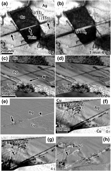
In MNCs with interface spacings above the submicron scale, dislocation pile-up against the interface, with resemblance to pile-up against the grain boundary in bulk metals, is proposed to be the major strengthening mechanism. The ability of the interface to block dislocation transmission is thus crucial in determining the mechanical properties of an MNC. To explore how interface properties affect dislocation transmission, Eftink et al. performed in situ tensile experiments on CuAg samples where the Cu/Ag interface is either cube-on-cube or incoherent twin [Reference Eftink, Li, Szlufarska, Mara and Robertson41]. By water quenching or directional solidification, the bi-layer thickness of CuAg was controlled at a few hundreds of nanometers. It was found that the cube-on-cube interface is a weak barrier to twinning partial dislocation, while the incoherent twin type interface effectively prevents partial transmission. As shown in Fig. 1(a), the deformation twin originated in Ag layer has propagated through the interface to the Cu layer, generating a continuous twin. With increasing strain in Fig. 1(b), the deformation twin thickens to the same extent in both phases, indicating that additional partial dislocations must have been generated at the interface. On the contrary, partial crossing the interface was not observed at the incoherent twin interface. Instead partials in Ag were absorbed by the interface, followed by emission of a perfect dislocation in Cu [Figs. 1(c)–1(e)] and dislocation pile-up in Ag followed by cross-slip of dislocations with no slip transmission, dislocation absorption into the interface, and emission back into the Ag layer [Figs. 1(f)–1(h)] was observed.
TEM images showing (a) continuous deformation twin across Cu/Ag interface, (b) thickening of the deformation twin in two phases, (c) generation of stacking faults in Ag with leading partials against the interface, (d) absorption of the leading and trailing partials by the interface, (e) emission of a perfect dislocation in Cu, (f) dislocation pile-up in Ag, (g) and (h) cross-slip of dislocations out of the pile-up and emission of dislocations back into Ag [Reference Eftink, Li, Szlufarska, Mara and Robertson41].

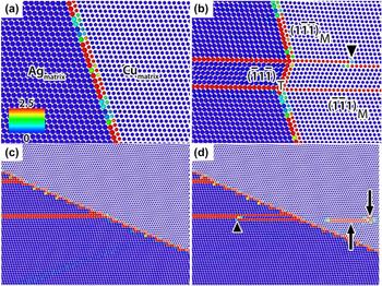
Molecular dynamic (MD) simulations were also conducted in this work to investigate dislocation–interface interactions at the two types of interfaces, which presented results in agreement with the in situ observation. At the cube-on-cube interface, the simulations showed transmission of twinning partial from Ag to Cu and rotation of the interface to transfer strain to the Cu layer, followed by thickening of the deformation twin by addition of mobile partial dislocations [Figs. 2(a) and 2(b)]. When a partial dislocation in Ag encounters an incoherent twin Ag/Cu interface, it is first accommodated by the interfaces without emission of dislocation, followed by nucleation of a new partial with opposite Burgers vector back into Ag and emission of two perfect dislocations into Cu [Figs. 2(c) and 2(d)].
MD simulations showing (a) initial cube-on-cube AgCu interface, (b) partial dislocation transmitted from Ag to Cu and the twin thickened from the partial dislocation indicated by the arrowhead, (c) partial dislocation in Ag accommodated by the interface and (d) nucleation of a partial back into Ag and emission of two perfect dislocations in Cu [Reference Eftink, Li, Szlufarska, Mara and Robertson41].
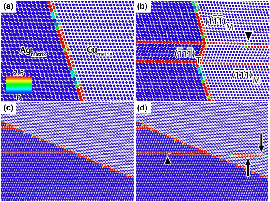
From this work, two general rules have been considered to predict dislocation–interface interaction behavior: (i) the geometric condition across the interface. This is described by the parameter m′ = cos(ϕ)·cos(κ), where ϕ is the angle between the slip plane normals and κ is the angle between the Burgers vectors of the incoming and outgoing dislocations. (ii) the magnitude of the Burgers vector of the residual interface dislocation,  $\left| {{b_{{\rm{res}}}}} \right|$. Dislocation transmission across the interfaces would be favored with a maximization of m′ and a minimization of
 $\left| {{b_{{\rm{res}}}}} \right|$.
Dislocation-confined layer slip mechanism
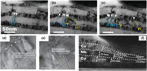
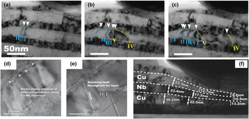
The breakdown of dislocation pile-up–based Hall–Petch model is typically inferred in multilayer MNCs when the layer thickness is in a few tens of nanometers, based on plots of measured hardness (or strength) as a function of  $\sqrt h$ [Reference Misra, Hirth and Hoagland7, Reference Foecke and Van Heerden42]. A CLS model constructed on earlier work of a similar mechanism in plastic yielding of thin films on substrates [Reference Freund43] was proposed to describe such deformation as glide of single Orowan-type dislocation loops bounded by the interfaces [Reference Misra, Hirth and Kung44]. To directly observe CLS and elucidate deformation mechanism in MNC when the feature size is of a few tens of nanometers, Li et al. performed in situ nanoindentation in TEM on quasi-single crystal Cu/Nb nanolayer films [Reference Li, Wang, Misra and Huang45]. The bilayer thickness of the film was 50 nm, with individual layer thickness of 20 nm for Nb and 30 nm for Cu and a {110} Nb//{111} Cu//interface plane texture. As shown in Figs. 3(a)–3(c), dislocation glide via CLS within the layers and nucleation of new dislocations were observed and ascribed as the dominant deformation mechanism in the material. Nucleation of dislocations at the Cu/Nb interface and emission of dislocation into the layer has also been observed, as demonstrated in Figs. 3(d) and 3(e). Interfaces were thus proposed to be the preferred nucleation sites for glide dislocations. Co-deformation of Cu and Nb nanolayers, which means simultaneous deformation of the two phases, was also observed without cracking to large plastic strains as shown in Fig. 3(f). This behavior is considered as the indicative feature of CLS, which has been discovered in various multilayer systems such as Cu/Zr [Reference Zhang, Lei, Liu, Niu, Chen, Liu, Zhang and Sun46], Cu/Au and Cu/Cr [Reference Li, Zhu, Tan, Wu, Wang and Zhang47]. No evidence of deformation twinning and dislocation transmission across the interface was encountered during the experiments.
In situ TEM study on Cu/Nb multilayer showing (a)–(c) confined layer slip and formation of new dislocations, (d, e) dislocation emission from the interfaces and (f) co-deformation of the nanolayers [Reference Li, Wang, Misra and Huang45].

Interface-mediated deformation twinning mechanism
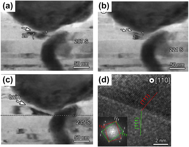
In accumulative roll-bonded (ARB) Cu/Nb multilayer MNC that has a Nb{112}//Cu{112} interface with the Kurdjumov–Sachs orientation relationship, deformation twinning was observed, in contrast to the above mentioned system with {110} Nb//{111} Cu//interface plane, although the interface spacing is similar [Reference Han, Carpenter, Wang, Beyerlein and Mara48]. To study the dynamic process of deformation twinning, Zheng et al. performed in situ TEM nanoindentation on such a system with a nominal individual layer thickness of 18 nm [Reference Zheng, Beyerlein, Wang, Carpenter, Han and Mara49]. As shown in Figs. 4(a) and 4(b), partial dislocation 1 emitted into Cu layer after loading, forming a stacking fault, followed by emission of partial dislocation 2 approximately 10 nm apart and formation of the second stacking fault. With further loading, twin formed between the two stacking faults as shown in Fig. 4(c). The HRTEM in Fig. 4(d) further confirms the formation of twin and demonstrates the twinning relationship across the twin boundary. From the in situ work and atomic scale analysis of the Cu/Nb interface, deformation twinning in ARB Cu/Nb can be described as first nucleation and emission of twinning dislocations from dissociation of misfit dislocations at the interfaces, the consequent formation of stacking faults separated along the interface, and the final nucleation and emission of twinning dislocations between the separated stacking faults.
(a)–(c) In situ TEM study on ARB process Cu/Nb multilayer showing formation of deformation twin from twin nuclei 1 and 2 and (d) HRTEM image at the twin boundary [Reference Zheng, Beyerlein, Wang, Carpenter, Han and Mara49].

Nanotwinning has been shown to be an effective strengthening mechanism in metallic materials with improved ductility [Reference Lu, Shen, Chen, Qian and Lu50, Reference Lu, Chen, Huang and Lu51, Reference Wei, Li, Zhu, Liu, Lei, Wang, Wu, Mi, Liu, Wang and Gao52]. In situ straining in TEM gives information on the origin of twinning from interfacial misfit dislocations. With a deeper understanding of the relationship between deformation twinning and the interface structure, twinning can be introduced to MNCs to improve their mechanical properties through interface design.
Room-temperature dislocation climb at interfaces
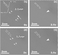
When the interface spacing is reduced down to a few nm, dislocation transmission across the interface is proposed to be the major deformation mechanism in MNCs. At this length scale, observation of dislocation line in TEM becomes very difficult. Instead, high-resolution (HR)-TEM is a useful tool to study dislocations at the atomic scale. When the indentation speed can be controlled below a few Å per second, in situ straining can be performed in HR-TEM mode. Li et al. conducted such experiments on Al/Nb multilayers with individual layer thickness of 5 nm with an indentation speed of 0.2 nm/s [Reference Li, Wang, Huang, Misra and Zhang53]. Snapshots at different instants during the tests in Fig. 5 illustrate that two dislocations approached from a 2.5 nm distance to 1.7 nm and finally annihilated each other along the interface through climb, which is unexpected in bulk Al or Nb at room temperature and provides experimental support to the atomistic simulation showing that dislocations could effectively climb near and within interfaces and facilitate dislocation transmission [Reference Wang, Hoagland and Misra54]. A near perfect interface was left after the annihilation. Based on the frame rate, a lower bound of the climb velocity could be estimated at 0.4 nm/s, which is two orders of magnitude higher than the climb velocity of ∼0.001 nm/s in bulk Al [Reference Liao, Srinivasan, Zhao, Baskes, Zhu, Zhou, Lavernia and Xu55]. Enhanced diffusion of vacancies and higher vacancy concentration at the interface were proposed to attribute to the rapid climb of dislocations at the interface [Reference Wang, Hoagland and Misra54]. Through this work, dislocation trapping at the interface, pinning of partial dislocation at the interface that leads to the extension of stacking fault, and increase of dislocation density from ∼1014 m−2 to ∼1016 m−2 after indentation, which should account for the large magnitude of plastic deformation in crystals, were also observed. These observations that were not attainable from other approaches provide important insight into understanding the deformation mechanisms in MNCs at fine length scale.
HRTEM snapshots showing (a) two dislocation b1 and b2 separated by 2.5nm; (2) b1 and b2 approaching each other through climb; (c) annihilation of the two dislocations and (d) the interface after dislocation annihilation.

Fracture mechanisms in multilayers
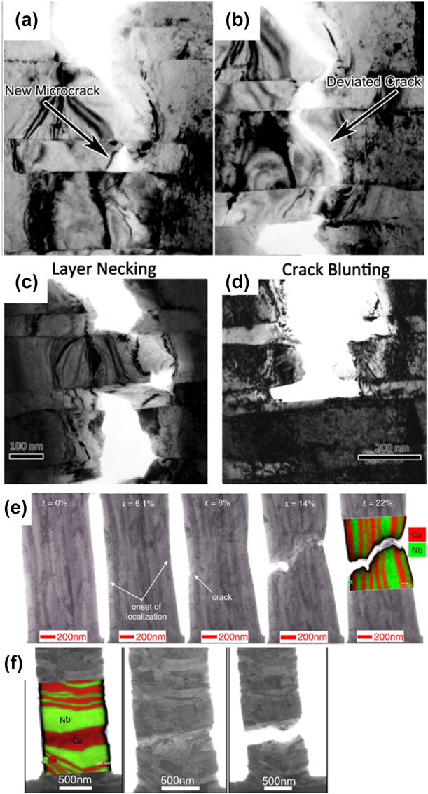
Besides tracing dislocation activities, investigation of the size and morphological evolutions of the nanosized phase is also enabled by the in situ TEM technique. Besides the evolution in layer thickness as mentioned above, crack propagation can also be observed, which provides an opportunity to study fracture mechanisms in situ in MNCs. Hattar et al. performed such experiment on multilayers of 65-nm Cu and 150-nm Nb by stretching the sample in TEM [Reference Hattar, Misra, Dosanjh, Dickerson, Robertson and Hoagland56]. Four crack hindrance mechanisms were observed, namely microvoid formation [Fig. 6(a)], crack deviation [Fig. 6(b)], layer necking [Fig. 6(c)], and crack blunting [Fig. 6(d)]. This work provided insight on the role of interfaces in impeding crack propagation. Coupling with the information gained from dislocation–interface interactions, deformation and fracture mechanisms of MNCs will be better understood.
TEM images showing (a) formation of microcrack, (b) crack deviation, (c) layer necking, and (d) crack blunting of 65 nm Cu/150 nm Nb MNC [Reference Hattar, Misra, Dosanjh, Dickerson, Robertson and Hoagland56], and snapshots from the tensile test on 63 nm Cu/Nb when the load is (e) parallel to the interface and (f) perpendicular to the interfaces [Reference Liu, Monclús, Yang, Castillo-Rodríguez, Molina-Aldareguía and LLorca57].

In the previous study, fracture mechanisms were only studied when the load was applied parallel to the interfaces. Liu et al. tested Cu/Nb multilayers in two loading orientations—parallel to the interfaces and also the perpendicular case [Reference Liu, Monclús, Yang, Castillo-Rodríguez, Molina-Aldareguía and LLorca57]. Their material was prepared through ARB to achieve an average layer thickness of 63 nm. Under parallel loading, CLS in both Cu and Nb was observed, leading to nearly isostrain co-deformation, until the onset of strain localization, which resulted in crack formation and propagation similar to Hatter’s observations [Fig. 6(e)]. When the load is perpendicular to the interfaces, deformation rapidly localized in a thicker Cu layer, which is supposed to be softer. Failure of the specimen was followed as shown in Fig. 6(f), giving an apparent “brittle” behavior. Stress and strain values were measured during the test and showed that when the load was applied parallel to the interfaces, the Cu/Nb multilayers had both higher strength and better deformability, owing to the ability of the interfaces to impede both dislocation glide and crack propagation.
Measurement of the shear strength of the interface
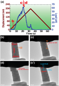
As mentioned in the previous example, in situ TEM sample holders not only serve to introduce strain to the sample, but the option of realtime load–displacement measurements is also available. The stress and strain values can thus be calculated during a dynamic process and related to corresponding deformation events. One important mechanical parameter of an MNC is the shear strength of the interface, which can be defined as the critical shear stress at which one layer slides with respect to the other along the interface plane. Atomic simulations have shown that the ability of a semicoherent interface to block dislocations is closely related to its shear strength [Reference Wang, Misra, Hoagland and Hirth11, Reference Hoagland, Hirth and Misra12]. When the interface is weak in shear, the stress field of a glide dislocation approaching the interface would locally shear the interface. In consequence, the glide dislocation is attracted to the interface and absorbed by it in the form of core spreading along the interface plane. Exceptionally high applied stress is required to re-nucleate a glide dislocation at the other side of the interface to complete the transmission. Although atomic simulations can give estimations on the interface shear strength, in situ nanopillar compression test offers a method to measure it directly, which is easily applicable to any metal systems. Li et al. fabricated nanopillars from Cu/Nb multilayers and shear loaded the pillar with the loading axis ∼25° off the stage axis to measure the Cu/Nb interface strength [Reference Li, Mara, Wang, Dickerson, Huang and Misra58]. Figure 7(a) presents the load/displacement data measured during the compression and Figs. 7(b)–4(d) are TEM image snapshots from the test, corresponding to points b to d in Fig. 7(a). The interfaces can be clearly resolved in the TEM images and thus sliding along the interfaces can be distinguished from shearing within the nanolayers. Interface sliding was observed from points c to d, from the load data and measured diameter of the pillar at the sliding interface, the shear strength of the interface could be measured at 0.3 GPa, which is lower than the shear strength of both metals and in good agreement with the atomistic simulations [Reference Wang and Misra8]. As a consequence, plastic deformation may be localized along the interfaces when there is enough resolved stress along the interface plane and leads to shear band formation and premature failure of the material [Reference Bhattacharyya, Mara, Dickerson, Hoagland and Misra9, Reference Mara, Bhattacharyya, Dickerson, Hoagland and Misra59].
(a) Displacement and load data record during the test, point b to d correspond to images b to d, (b) to (d) in situ TEM study on Cu/Nb multilayer showing shearing at the interface [Reference Li, Mara, Wang, Dickerson, Huang and Misra58].

Assisting new morphological design for high strength and plasticity
Nanolayer MNCs, at interface spacings less than approximately 5 nm, are prone to strain localization in the form of shear band formation. One approach to promote plastic deformability in MNC is through new design in morphology. Recent work in our group has demonstrated that via co-sputtering of two immiscible metals, MNC with controlled morphology can be fabricated [Reference Derby, Cui, Baldwin and Misra60]. The prototype thin-film nanocomposites were only deposited to 1 micrometer thickness. Nanopillar compression test in TEM provides a means to characterize the mechanical properties of these MNCs [Reference Cui, Derby, Li, Mara and Misra13]. Figure 8(a) shows a scanning TEM (STEM) image of a nanopillar from 3 nm Cu/Mo multilayers after compression. Cu appears darker in the image compared to Mo because of its lower atomic number. It can be observed that localized shearing occurred at the top of the pillar. Figure 8(b) shows a Cu/Mo nanocomposite with a hierarchical structure, where Cu islands are distributed in matrix of alternating 3-nm Cu and 4-nm Mo ligaments. The STEM image of a nanopillar of the nanocomposite before and after 12% compression can be found in Fig. 8(c). No evidence of shear band was observed and a maximum flow stress of 2.6 GPa was observed. The Cu islands were observed to accommodate the plastic strain and supposed to avert shear localization. Another work that was carried out in the scanning electron microscope (SEM) but worth mentioning here is that with a bicontinuous interpenetrating structure as shown in Fig. 8(d), the pillar compression test showed high stress level over 2 GPa up to 30% compression [Reference Cui, Derby, Li and Misra61]. An STEM image of the pillar after compression is shown in Fig. 8(e), uniform distribution of deformation can be observed in the bicontinuous structure.
STEM images showing (a) 3 nm Cu/Mo multilayer nanopillars after compression test, (b) cross-section of the hierarchical Cu/Mo nanocomposite, (c) nanopillar of the hierarchical nanocomposite before and after compression test, (d) cross-section of the bicontinuous structure, and (e) nanopillar of the bicontinuous structure after compression test where the original diameter is shown by the dotted lines [Reference Cui, Derby, Li, Mara and Misra13, Reference Cui, Derby, Li and Misra61].

In situ straining in TEM can adequately test the mechanical properties of samples fabricated at small scale. The above examples reveal that a hierarchical and bicontinuous morphology would improve the plastic deformability of the Cu/Mo system while maintaining the high strength. Apart from nanopillar compression test, tensile, three-point bend, and other mechanical testing can also be performed. The challenge lies in sample preparation and manipulation at this small-length scale and interpretation of the experimental data considering the size effect of the mechanical behavior of a material.
Summary and conclusions
In situ straining in TEM has enabled the direct observation of deformation behavior of MNCs at the nano and atomic scales. Different modes of dislocation activities have been elucidated, which include dislocation pile-up, glide of single dislocations between interfaces, emission of dislocations from the interfaces, deformation twinning originated from interfacial dislocations, trapping of dislocations at the interfaces, and dislocation climb at the interface. These activities are directly related to the mechanical properties of the MNCs. A better understanding of the deformation mechanisms based on the information provided by in situ tests will give us guidance on designing MNCs with desired mechanical properties. Quantitative in situ tests enable direct measurement of the mechanical parameters of an MNC, facilitating the design process. Most of the in situ work on MNCs were performed in compression mode, and results from tensile and bending tests will be reported in the future.
The development in the in situ instrumentation will further enable us to investigate the response of nanocomposites under various conditions like repeated loading, high strain rate, corrosive environment, elevated temperature, and irradiation. A more complete dataset of the mechanical properties of an MNC will be achieved, and the design of MNCs can be targeted to specific applications. Faster imaging techniques working at millisecond to microsecond time scale will enable collection of clearer images during the dynamic deformation process.
Acknowledgments
YC and AM acknowledge the support from NSF under the DMREF program [Grant No. 1533557]. Electron microscopy was performed at the Michigan Center for Materials Characterization operated by the College of Engineering, University of Michigan. This work was performed, in part, at the Center for Integrated Nanotechnologies, an Office of Science User Facility operated for the U.S. Department of Energy (DOE) Office of Science. Los Alamos National Laboratory, an affirmative action equal opportunity employer, is managed by Triad National Security, LLC for the U.S. Department of Energy’s NNSA, under contract 89233218CNA000001. The authors are grateful for discussions with M.J. Demkowicz, J. Wang, J.K. Baldwin, B. Derby, and K. Sun.