Introduction
Metasurface, a novel type of two-dimensional (2D) metamaterial, has gained increasing attention due to the unique abilities in light manipulation.[ Reference Yu and Capasso 1 ] In contrast to the phase changes via propagations in conventional systems, metasurface can introduce abrupt changes on both phase and amplitudes of waves via arrays of optical resonators.[ Reference Kildishev, Boltasseva and Shalaev 2 ] In this sense, the dependence of propagation effects can be simply released and thus a number of novel 2D devices have been proposed and experimentally demonstrated in past few years, e.g. anomalous reflection/refraction.[ Reference Yu, Genevet, Kats, Aieta, Tetienne, Capasso and Gaburro 3 , Reference Ni, Emani, Kildishev, Boltasseva and Shalaev 4 ] surface-wave coupling,[ Reference Sun, He, Xiao, Xu, Li and Zhou 5 ] high-resolution optical hologram,[ Reference Larouche, Tsai, Tyler, Jokerst and Smith 6 ] and the well-known flat lens.[ Reference Huang, Chen, Mühlenbernd, Zhang, Chen, Bai and Zhang 7 , Reference Aieta, Genevet, Kats, Yu, Blanchard, Gaburro and Capasso 8 ] The initial metasurfaces are designed and realized in arrays of metallic resonators. But the huge intrinsic losses of metal have strongly limited the converting efficiency,[ Reference Pors, Nielsen, Eriksen and Bozhevolnyi 9 , Reference Aieta, Kats, Genevet and Capasso 10 ] especially in near-IR and visible wavelength range. To improve the reflection coefficient, all-dielectric metasurfaces have been proposed and fabricated by replacing plasmonic resonances with Mie scattering resonances.[ Reference Yang, Wang, Moitra, Kravchenko, Briggs and Valentine 11 – Reference Lin, Fan, Hasman and Brongersma 13 ] Silicon metasurfaces are the most prominent examples due to the high refractive index and low loss of silicon.[ Reference Yang, Wang, Moitra, Kravchenko, Briggs and Valentine 11 ] In past few years, more than 98% conversion efficiency over a 200 nm bandwidth has been successfully demonstrated in the near-IR wavelength range.[ Reference Yang, Wang and Moitra 14 ] Low loss and achromatic silicon flat lens have also been realized by several groups.[ Reference Moitra, Slovick, Li, Kravchencko, Briggs, Krishnamurthy and Valentine 15 – Reference Ou, Plum, Jiang and Zheludev 17 ] All these achievements have clearly shown the bright futures of silicon metamaterials. However, the researches on silicon metamaterials are facing severe challenges when the working wavelengths are shifted to visible frequency range.
Because of the high refractive index and wide band gap (anatase 3.2 eV and rutile 3.0 eV), titanium dioxide (TiO2) has been considered as an alternative materials for all-dielectric metasurfaces in visible range. In past few years, several techniques and methods have been developed to deposit TiO2 thin films, e.g. electron beam evaporation,[ Reference Yao, Huang and Ma 18 ] sol–gel method,[ Reference Sonawane, Hegdeand and Dongare 19 ] magnetron sputtering technique,[ Reference Löbl, Huppertz and Merge 20 ] and pulsed laser deposition.[ Reference Suda, Kawasaki and Ueda 21 ] Among all these approaches, electron beam evaporation has shown several intrinsic advantages. It can produce large area high-quality optical films with low defect density, low cost, and high repeatability. Most importantly, electron beam evaporation is highly directional and thus is compatible with the current lift-off process of fabricating metasurfaces. However, the flux of atoms impinging on the substrate is lower that with other methods such as magnetron sputtering. Therefore, the refractive index of the as-deposited layer is expected to be <2.3.[ Reference Sarakinos, Alami, Klever and Wuttig 22 ] This refractive index is good enough for some applications such as multilayer distributed Bragg reflector. But it is relatively low to realize dielectric-based metasurface at the visible range.
Here we demonstrate the fabrication of high-quality TiO2 with electron beam evaporation. By changing the post-annealing temperature and oxygen ambient, uniform TiO2 films with large area have been successfully obtained. The real part of refractive index is almost 2.4 at 632 nm, while the corresponding imaginary part is around zero through the whole visible range. Our further numerical calculation shows that the optical properties of TiO2 films are good enough to precisely engineer the phase of the reflected light over the whole 2π range.
Fabrication
TiO2 thin films are deposited on the p-type Si (1 0 0) substrate by electron beam evaporator (Syskey Co., Ltd.). Before the deposition, silicon wafers are firstly washed in deionized water, acetone, and isopropyl alcohol by sonication for 15 min each, and then blow-dried by clear dry air (CDA). TiO2 [99.999%, ZhongNuo Advanced Material (BeiJing) Technology Co., Ltd.] is deposited on the silicon wafers by electron beam evaporator with a fixed rate at 1 A/s. The thickness of TiO2 films are controlled by the deposition time. The electron gun operating voltage is 5.2 kV, and the current of beam is 4.5 mA. The vacuum of our system is below 5.0 × 10⁻⁵ Pa. The substrate temperature during deposition is kept at 200 °C, which is an optimized value by measuring the refractive index of the TiO2 film as a function of substrate temperature. The as-prepared sample is named as TiO2@Si. After the preliminary deposition, the TiO2@Si films are annealed in an annealing furnace with oxygen atmosphere for 90 min. The post-deposition annealing (PDA) is performed at different temperature ranging from 300 to 900 °C with 200 °C interval and kept for 90 min in oxygen ambient following by a naturally cooling down process.
The thickness and the surface morphology of TiO2 thin films are measured using a field emission scanning electron microscope (FE-SEM, Model S-4700, Hitachi, Japan). The chemical composition of the TiO2 films are investigated using an energy-dispersive X-ray spectroscopy (EDS) equipped on FE-SEM. The microstructures of the various films are examined using an X-ray diffraction (XRD) system (Model ATX-E, Rigaku) with Cu K α radiation and a standard Bragg–Brentano geometry (θ–2θ). The optical properties of the TiO2 film are investigated using a Rotating Compensator Ellipsometer (VASE M2000U, J.A. Woollam).[ Reference Kotake, Jiaand and Nakamura 23 ]
Characterization of the TiO2 film
Composition and surface morphology
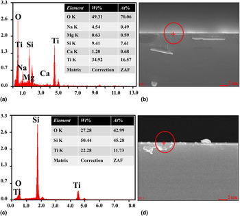
It is well known that the composition of the titanium oxide thin films have a significant effect on the optical properties.[ Reference Bendavid, Martin and Jamting 24 ] We then study the compositions of deposited TiO2 films. Figure 1 show the experimental results of two samples which are annealed at 200 °C (Sample A) and 500 °C (Sample B) in oxygen, respectively. Both of their thicknesses are 50 nm. Figures 1(a) and 1(c) show the compositions of these two films that are measured with EDS. The molecular content of the oxygen is about 3.408 times of that of titanium when the film is annealed at 200 °C. When the annealing temperature is increased to 500 °C, the molar ratio of oxygen to titanium is very similar (~3.66). The molar ratios of oxygen to titanium are more than 2:1 in both samples and no obvious difference can be observed. This indicates that the TiO2 films have a stable chemical composition near to that of TiO2 after annealing in oxygen environment.
EDS spectrum of the deposited TiO2 film with 50 nm thickness annealed in oxygen at 200 °C (a, b) and 500 °C (c, d).

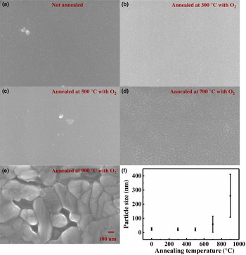
Unlike the chemical component, the morphology of the films can be effectively modified by the PDA. To test the effect of PDA, we have deposited a series of TiO2 films and annealed at different temperature in oxygen ambient. The thicknesses of all these films are kept at 50 nm. The morphologies of films are characterized with FE-SEM. All the results are summarized in Fig. 2. When the PDA temperature is below 500 °C, the TiO2 is quite uniform under the SEM image [see Figs. 2(a)–(c)]. When the annealing temperature is 700 °C, the particle size becomes larger and obvious reunited small grains can be observed [see Fig. 2(d)]. The changes in particle sizes have been analyzed and plotted in Fig. 2(f). We can see that the grain sizes increase with the temperature slowly at low temperature. Once the annealing temperature is increased to 700 °C, the grain size will increase very fast. When the PDA temperature is 900 °C, the small grains reunite and their final sizes are even as large as 100–400 nm. In principle, larger grain size will decrease the grain boundary defect density. According to previous reported,[ Reference Sun, Yi, Yao, Song and Xiao 25 ] larger real part of refractive index can be obtained by increasing the grain size of the TiO2 film. However, the increase of grain size will introduce a lot of defects and generate strong scattering loss. Therefore, the PDA temperature should be optimized.
Top-view SEM image of the TiO2 films with different PDA temperatures. (a) No annealing, (b) annealing at 300 °C, 90 min, oxygen ambient. (c) Annealing at 500 °C, 90 min, oxygen ambient. (d) Annealing at 900 °C, 90 min, oxygen ambient. (e) Annealing at 700 °C, 90 min, oxygen ambient. (f) The size distribution of gains in TiO2 film.

Microstructure
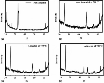
Besides the morphology, the crystalline structures of TiO2 thin films have a significant effect on the optical properties. Here the crystalline structure of the TiO2 films are examined with XRD, where a Nifiltered K α (λ = 1.54056 Å) is used. Figure 3 shows the XRD patterns of the films under different annealing conditions. A dominant peak with 2θ~33.382 appears for the as-deposited film, indicating the existence of the α–phase titanium. After annealing the films in oxygen under different temperatures, the peaks are presented with 2θ~25.382 and 2θ~48.31 attributing to the (101) plane of the anatase phase. This clearly shows that the crystalline properties have been improved with PDA. When the TiO2 is annealed at 900 °C, two new peaks with 2θ~44.38 and 2θ~55.24 appear [see Fig. 3(d)]. These new peaks are attributed to the rutile phase of TiO2. But the anatase phase still dominates the crystal structure of the film and the anatase crystallites preferentially grow with a strong orientation in the direction normal to (101) plane.
XRD patterns of the deposited films as a function of annealing temperature: anatase (A) and rutile (R). (JCPDS number 84–1286, 01–1292). (a) Annealing at 500 °C, 90 min, oxygen ambient. (b) Annealing at 500 °C, 90 min, oxygen ambient. (c) Annealing at 700 °C, 90 min, oxygen ambient. (d) Annealing at 900 °C, 90 min, oxygen ambient.

Ellipsometry measurement results
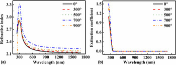
Based on the above experimental results, we know that the PDA can improve the crystal quality and the increase in the grain size. Therefore, the optical properties such as refractive index can be effectively changed by changing the PDA temperature. The thickness, refractive index, and extinction coefficient are examined by ellipsometry. Figure 4 shows the dispersion for the relations refractive index n(λ) and the extinction coefficient k(λ) of TiO2 films under different annealing conditions as a result of the theoretical fit to spectroscopic ellipsometry. The thickness of the films decreases in turn with the increase of the annealing temperature from 55 to 50 nm, with 10% thickness change. The real part of the refractive index shows an upward tendency with the increase of the annealing temperature. The specific real part of the refractive index increase in turn from n = 2.2 for 300 °C to n = 2.4 for 700 °C at the wavelength of 632 nm, which is already the highest value that can be obtained using the electron beam deposition method. Further increase the annealing temperature to 900 °C will decrease the effective refractive index on the contrary way. This kind of changes in refractive index is understandable. As we mentioned above, the improved crystal quality can increase the refractive index. However, more air defects are formed when the film is annealed at 900 °C [see the SEM image in Fig. 2(e)]. Thus, the averaged refractive index is decreased. For all the films under different annealing parameters, the extinction coefficients stay at very low value. This is mainly because that the thickness of TiO2 film is very small and TiO2 is transparent in the visible and near IR wavelength range. However, we can still see the obvious increase of extinction ratio in Fig. 4(b) when the PDA temperature is 900 °C. This is also consistent with the SEM image in Fig. 2(e) well. To now, we can determine the PDA temperature at 700 °C as the optimized condition for high-quality TiO2 film. As shown in Fig. 4, relative uniform film with refractive index n = 2.4 at 632 nm can be achieved. Meanwhile, its extinction ratio is as good as conventional un-annealed film and can be neglected in visible range.
(a) Refractive index dispersion of TiO2 films annealed at various temperatures. (b) Extinction coefficients of TiO2 films annealed at various temperatures.

Metasurface design with TiO2 as composition material
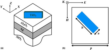
After achieving high refractive index TiO2 film, we thus can use it to design the metasurface at visible light range. To focus light, it is important to create 0–2π phase shifts and modulate the amplitude of light. In flat lens, this can be achieved using the resonances of sub-wavelength dielectric antennas with high refractive index and low loss. Then we start our design by numerically analyzing the resonant characteristics of periodically aligned antenna using TiO2 as a building material with a commercial finite-element package COMSOL Multiphysics. The schematic structure of antenna is depicted in Fig. 5(a). It is composed of a TiO2 rectangular block and a 150 nm silver ground plane, which are separated by a 150 nm alumina spacer. The thickness and refractive index of TiO2 rectangular block are set at 240 nm and the refractive index is taken directly from the retrieved result from the experiment. The geometry and high refractive index are properly chosen in order to excite the Mie resonance in the visible region. The refractive index of the alumina space layer and the substrate is n Al2O3 = 1.62. The optical properties of silver are taken from Jonson's experiments.[ Reference Sun, Yi, Yao, Song and Xiao 25 ] The in-plane width and length of rectangular antenna are denoted by a and b, which determine the amplitudes and phases of resonant modes of the antenna well. A normal incident plane light is used to excite the antenna from the air side. The polarization of incident light is linear polarized along the x-axis, which is tilted 45° with respect to the silicon block [see Fig. 5(b)].
Unit cell of the TiO2 metasurface. (a) Schematic representation of the TiO2 nanoantennas unit cell. (b)Top view of the unit cell.

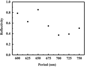
Periodic boundary condition is used in our simulations. As it is shown in Fig. 6, with the change of the period, the reflective amplitudes of light will also change, and the highest reflection can be obtained with period p = 650 nm. As a result, the periodicity of unit cell is set as 650 nm in our following simulations.
The period-dependent reflection of antenna array with a = 275 nm and b = 375 nm.

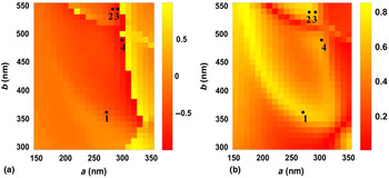
A 0–2π phase shifts are most important for design metasurface with ability to focus the incident light with flat surface. Based on the fact that reflection spectrum is mainly formed by the resonances in rectangular TiO2 antenna, the phase and amplitude of the reflected cross-polarized light can be efficiently controlled by changing the nanostructure's length a and width b, at a fixed wavelength of 632 nm. Figure 7(a) and 7(b) show the 2D color maps of calculated phase (φ cross) and reflectance (|r cross|2) with different a and b. Here the simulation wavelength is 632 nm. In Fig. 7(a), a region with high reflection efficiency (|r cross|2 > 0.5) can be clearly observed. Interestingly, the corresponding phase shifts in Fig. 7(a) covers a wide range from 0 to 2π. Consequently, the high reflection and 0–2π phase shifts can be obtained simultaneously. As a result, we can choose four antennas which provide an incremental phase shift of π/4 for cross-polarized reflected light shown as black points in Fig. 7. By simply rotating the structures by 90° counter clockwise, the additional π-phase shift can be attained. Therefore, the rectangular TiO2 antenna array can realize the whole phase shifts from 0 to 2π while maintaining near-equal amplitude. The results shown in Fig. 7 are general rather than application specific, and therefore, they can be used to design a number of functionalities like anomalous reflection, and flatlens for focusing and spectrum splitting.
Reflection properties of antennas. Variations of the reflectance phase (in the unit of π) (a) and amplitude (b) with a and b.

Conclusion
In conclusion, a high refractive index TiO2 film is grown by electron beam evaporation and post annealing at 700 °C. Due to the optimized crystal structure, grain size, packing density, and roughness of film, an averaged refractive index of TiO2 film is larger than 2.4 at 632 nm. Based on the refractive index of TiO2 film, a metasurface at visible light range can be designed. Our calculation shows that our TiO2 film is good enough to support 0–2π phase shift. We believe that our results will be important for the development of metasurfaces operating at visible range.
Acknowledgments
This work is supported by NSFC under the grant numbers 11374078, Shenzhen peacock plan KQCX20130627094615410, and Shenzhen Fundamental research plan under the grant numbers JCYJ20130329155148184, JCYJ20140417172417110, and JCYJ20140417172417096.