I. INTRODUCTION
Diamond-like carbon (DLC) has a unique combination of properties including extreme hardness, optical transparency, high electrical resistivity, and chemical inertness, and it is therefore widely used for a variety of applications such as biomedical engineering, protective coating, microelectromechanical systems, cutting tool, antireflective coating, and as a field emission source for emitter.Reference Fallon, Veerasamy, Davis, Robertson, Amaratunga, Milne and Koskinen1–Reference Nakatani, Okamoto, Omura and Yamashita5 There are also several types of bonds in DLC that confer a wide range of properties. DLC is an amorphous carbon material with sp 2- or sp 3-bonded carbon and hydrogen. The chemical structure of DLC, which corresponds to a bond ratio of sp 3:sp 2, is important because it produces the unique properties of DLC.Reference Robertson6 The strong directional sp 3 bonding of diamond gives it many unique properties such as extreme hardness, optical transparency, high electrical resistivity, and chemical inertness. In contrast, the sp 2 bonding of graphite produces weak interlayer bonding, making it useful as a lubricant.Reference Robertson6 The properties of DLC have been reported to be significantly dependent on the deposition conditions because the energy of carbon species plays an important role in determining the sp 3:sp 2 ratio in DLC films.Reference Voevodin and Donley7, Reference Tsai and Bogy8 Also, incorporation of Si, B, N, and F into DLC films has been shown to change the sp 3:sp 2 ratio. Addition of Si and F shows different behavior on the change in the ratio of sp 3:sp 2 DLC. For example, an addition of Si increases the sp 3:sp 2 ratio but an addition of F decreases the ratio.Reference Jung and Park9, Reference Jung and Park10 As the proportion of sp 2 bonds increases, the electrical conductivity of the DLC film increases but the diamond-like properties decrease. If the diamond-like properties of the film could be maintained while enhancing the electrical conductivity, the DLC films could be used for chemical sensing, electrosynthesis, electrochemical-based toxic waste detection, remediation, and so on.Reference Lee, Tryk, Fujishima and Park11 The higher energy of the carbon species increases the sp 3 bonding ratio, and the addition of B into DLC increases the sp 2 bonding ratio in the film and N maintains the formation of the sp 3 bond.Reference Sikora, Bourgeois, Sanchez-Lopez, Rouzaud, Rojas, Loir, Garden, Garrelie and Donnet12, Reference Jung and Park13 Furthermore, an increase in hardness has also been reported with the addition of N into the carbon due to the formation of a crystalline β-C3N4phase with highly enhanced mechanical and chemical properties.Reference Liu and Cohen14, Reference Gu, Zhang, Duan, Chang, Tian, Chen, Dong, Shi, Zhang and Yuan15
In this paper, we report the effects of B and N codoping on the hardness and electrical resistivity of DLC films grown on thermally grown SiO2 on Si substrate by magnetron sputtering deposition. The electrical conductivity and hardness of the N–B codoped DLC films were simultaneously controlled through a neutralization effect of N and B codoping by varying N2 flow rate with fixed B target power and varying B target power with fixed N2flow rate. The films were examined using hall measure equipment, nanoindentation, scanning electron microscopy (SEM), and x-ray photoelectron spectroscopy (XPS).
II. EXPERIMENTAL PROCEDURES
Nitrogen and boron codoped DLC films were fabricated by RF magnetron sputtering deposition. 100-nm-thick SiO2 layer thermally grown on Si wafers was used as a substrate. High-purity graphite (99.999 wt%) and boron (99.97 wt%) targets with 2-inch diameters were mounted on the cathode. The distance between the target and the substrate was 6 cm. The background pressure was approximately 3.9 × 10⁻⁴ Pa, and the sputtering was conducted under N2 and Ar atmosphere with a total pressure of 1.9 Pa. The total flow rate of the mixed gases was fixed at 607.9 (Pa m3)/s, and the flow rate of the N2 gas was varied from 0 to 60.7 (Pa m3)/s. The RF power of the carbon was fixed at 100 W and that of boron was varied from 0 to 25 W. The substrate was kept at room temperature. The targets were degassed before sputtering for 5 min and after sputtering for 300 min. The deposition rate was measured using cross-sectional SEM (JSM 7001F; JEOL,Tokyo, Japan). XPS (VG Escalab 220i-XL; Thermo VG Scientific Ltd., West Sussex, UK) was used to analyze the elemental composition and the chemical bonding state. 1486.6 eV of monochromatic Al Kαradiation with 0.47 eV of width was used, and emitted photoelectrons were detected with hemispherical analyzer at a pass energy of 15 eV. Hall measurement equipment was used to measure the electrical resistivity of the DLC films, and nanoindentation was used to measure the hardness of the DLC films. For nanoindentation measurement, Berkovich indentation tip made by ISO 14577 was used to track the hardness. The averaged hardness data were obtained after analysis for 9–10 times. The strain rate target was chosen as 0.05/s for all samples. The total measurement time was approximately 300 s at a time, and the maximum load for each sample was varied from 142 to 161 mN.
III. RESULTS AND DISCUSSION
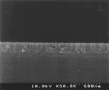
First, B-doped DLC films were fabricated by adjusting B target power to determine the proper N-doping amount for B-doped DLC film. A cross-sectional SEM image of B-doped DLC film as shown in Fig. 1 revealed that about 250-nm uniform thick film was successfully formed. The conditions of sputtering were 100 W (graphite target power), 15 W (boron target power), 607.9 (Pa m3)/s (Ar gas flow rate), and 300 min (deposition time).
Cross-sectional SEM images of the B-doped DLC film.

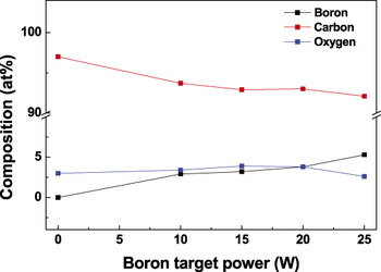
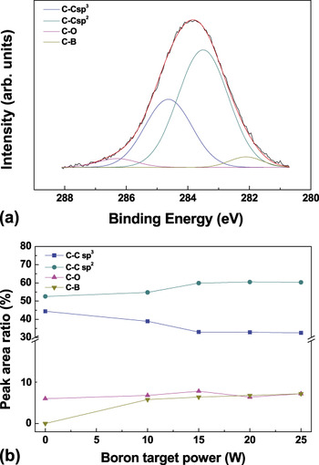
The effect of boron target power on the composition of B-doped DLC films was determined by XPS analysis. As shown in Fig. 2, the variation in the composition of B in the B-doped DLC films was a function of the boron target power: 2.9–5.3 at.% of B with 10–25 W of target power. The effect of B concentration on the evolution of the chemical bonding state could be deduced from C 1s XPS core-level spectra. To determine the relative intensity of each contribution precisely, deconvolution of the spectra was achieved using a Gaussian/Lorentzian function as shown in Fig. 3(a) for 15 W of B target power. The decomposed peak with binding energies of 282.5, 284, 285, and ∼286.5 eV were assigned to C–B, C–C sp 2, C–C sp 3, and C–O bonding states, respectively.Reference Lee, Tryk, Fujishima and Park11, Reference Díaz, Anders, Zhou, Moler, Kellar and Hussain16 A small amount of C–O bonding was also observed in the spectra at the binding energy of ∼286.5 eV due to contamination from air exposure. The relative deconvoluted peak ratio in Fig. 3(b) shows that the C–B bonding contribution was increased according to B target power due to an increase in B content. We also observed that the reduction in C–C sp 3 bonding became important with increasing B target power due to the enhanced graphitization of carbon by the substitution of C with B until 15 W of B target power. Normally, B is introduced into both substitutional and interstitial positions in the prepared B-doped DLC.Reference Marinković, Sužnjević and Dežarov17, Reference Ottaviani18 By entering substitutionally, B acts as a graphitization catalyst but has an inverse effect when present in an interstitial position.Reference Marinković, Sužnjević and Dežarov17 The reduction in C–C sp 3 bonding was not increased with a B target power higher than 15 W, as shown in Fig. 3(b). This might be due to the substitutional limit of B in DLC because an excess amount of B above the limit does not induce a graphitization of DLC.Reference Ottaviani18
Variation in the composition of the B-doped DLC films with different B target powers.

(a) Deconvoluted x-ray photoelectron spectra of C 1s of B-doped DLC films with 15 W of B target power and (b) deconvoluted C 1s peak ratio with different B target powers for the B-doped DLC films.

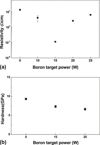
The effect of reduction in C–C sp 3 bonding on the electrical and mechanical properties of B-doped DLC films was analyzed using Hall measurement equipment and nanoindentation, respectively. The variation in the resistivity and hardness of the B-doped DLC film is shown in Figs. 4(a) and 4(b). The electrical conduction in DLC can be described by thermal hopping and electron tunneling through localized C–C sp 2 bond sites.Reference Hauser19 This is due to the fact that the energy of bonding electron in C–C sp 2-bonded C atoms exists near the Fermi level. Therefore, the number of C–C sp 2 bonds increases as the B content increases, and the hopping distance is likely to be shortened, resulting in a lower resistivity. In addition, the strong directional sp 3 bond in diamond provides greater hardness.Reference Robertson6 Also, the values for resistivity and hardness of B-doped DLC decrease with increases in B doping due to an increase in C–C sp 2 content and a decrease in C–C sp 3 content. The minimum value for resistivity was obtained with 15 W of B target power, i.e., approximately 3 at.% B content. As shown in Fig. 4(b), the resistivity increased after 15 W of B target power because an excess amount of B above the substitutional limit can induce the formation of a B4C phase, which has a higher resistivity than the graphite phase (e.g., a resistivity of 0.1–10 Ωcm).Reference Pierson20
Variation in the (a) electrical resistivity and (b) hardness of the B-doped DLC films with different B target powers.

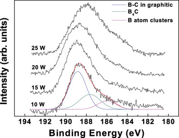
Figure 5 shows B 1s photoelectron peaks in DLC films according to B target powers. The decomposed B 1s peaks with binding energies of 189, 187.6, and ∼186 eV were assigned to B–C, B4C, and B atom cluster bonding states, respectively.Reference Rodriguez and Baker21 With increasing B target power, an increase in the B4C component of the total intensity was observed, and a contribution from B atom cluster was also found. The resulting change in the bonding constitution of B with the target power is in agreement with the resistivity results given in Fig. 4(b). The B doping condition of 15 W of target power was selected for preparing N–B codoped DLC films.
B 1s XPS spectra of the B-doped DLC films with different B target powers.

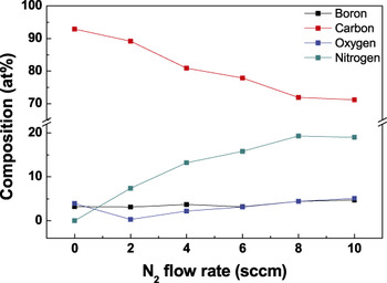
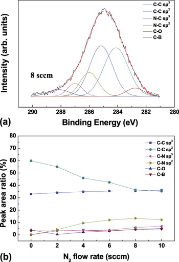
A comparison of the normalized area intensities of C 1s, B 1s, N 1s, and O 1s peaks in the XPS spectra was carried out to investigate the effect of N2 gas flow rate on the variations in the composition of N–B codoped DLC films. Figure 6 shows the XPS composition results as a function of N2 flow rate from 0 to 607.9 (Pa m3)/s. The nitrogen content in the N–B codoped DLC film increased up to N2 flow rate of 48.6 (Pa m3)/s, around 19 at.%, and after that, the nitrogen content was almost saturated. The effect of N incorporation on the bonded constituents of the B-doped DLC film prepared with 15 W of B target power is shown in Fig. 7(a). Based on the previous results, the decomposed peaks with binding energies of 282.5, 284, 285, 286, 288, and ∼289 eV were assigned to C–B, C–C sp 2, C–C sp 3, N–C sp 2, N–C sp 3, and C–O bonding states, respectively.Reference Lee, Tryk, Fujishima and Park11, Reference Souto, Pickholz, dos Santos and Alvarez22 The variation in the bonded constituents as a function of N2 flow rate is shown in Fig. 7(b), and the relative intensity of C–N bonding constituents, e.g., N–C sp 2 and N–C sp 3 bonding peaks, increased as the N2 flow rate increased. From a rapid reduction in C–C sp 2 bonding peak with increasing N2 flow rate, N atoms were found to preferentially substitute for C in the C–C sp 2bond.
Variation in the composition of N–B codoped DLC films with different N2flow rates.

(a) Deconvoluted x-ray photoelectron spectra of C 1s of N–B codoped DLC films prepared using 15 W of B target power and a N2 flow rate of 48.6 (Pa m3)/s and (b) deconvoluted C 1s peak ratio in N–B codoped DLC films prepared using 15 W of B target power and different N2flow rates.

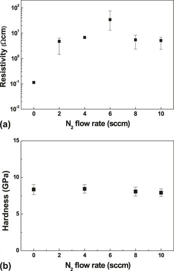
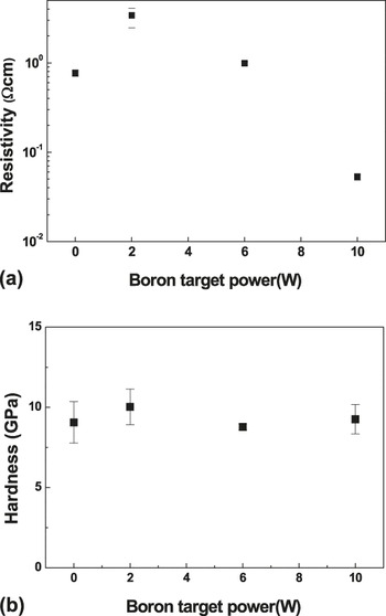
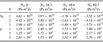
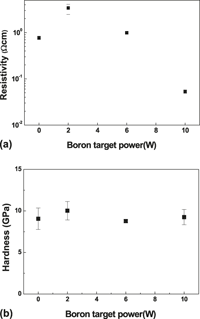
Variations in the resistivity and hardness of the N–B codoped DLC films according to the N2 flow rate were monitored using Hall measurement equipment and nanoindentation [Figs. 8(a) and 8(b)]. The number of C–C sp 2 bonds decreased as the N2 flow rate increased, causing the hopping distance to lengthen, which resulted in high resistivity.Reference Hauser19 Furthermore, the incorporation of N may neutralize the doping effect of B. However, at a N2 flow rate greater than 36.4 (Pa m3)/s, the resistivity decreased, possibly due to a change in the conduction type of N–B codoped DLC (Table I). The incorporated nitrogen could also act as a n-type dopant. However, in the case of the hardness measurements, despite an increase in N content in the DLC film, the hardness was not increased as expected.Reference Liu and Cohen14 A constant hardness, even with an increase in N content, should be a characteristic of N–B codoped DLC films. As previously mentioned, the incorporation of N neutralizes the effect of B doping. As a result, the decreased electrical resistivity and reduced hardness of the DLC film with incorporated B reincreased or at least stayed the same with the incorporation of N. To confirm the neutralization effect between N and B, the electrical resistivity and hardness of N–B codoped DLC films were measured with the samples prepared under a N2 gas flow rate of 24.3 (Pa m3)/s with varying B target powers. As shown in Fig. 9(a), the electrical resistivity of the N-doped DLC film increased with B codoping but decreased with more than over 2 W of B target power. This convex behavior of the electrical resistivity with B target power could be explained by the neutralization effect of N by B at low target power and the B doping effect at high power. The hardness of N-doped DLC films according to B codoping is shown in Fig. 9(b). Hardness was almost uniform with increasing B target power until 10 W, and this behavior was due to the neutralization effect between N and B; a decrease in the hardness due to an increase in B was compensated by the addition of N. Based on these observations, it can be said that N–B codoped DLC films with optimized mechanical and electrical properties can be obtained from the compensation effect of the dopants.
Variation in the (a) electrical resistivity and (b) hardness of N–B codoped DLC films prepared using 15 W of B target power and different N2flow rates.

Variation in the (a) electrical resistivity and (b) hardness of N–B codoped DLC films prepared using a N2 gas flow rate of 24.3 (Pa m3)/s with different B target powers.

Electrical property of N–B codoped DLC films as a function of N2 flow rate. (N b, carrier concentration; μ, carrier mobility; N, number of measurements.)

IV. CONCLUSIONS
N–B codoped DLC films were prepared using RF magnetron sputtering. The bonding state, hardness, and electrical resistivity of the DLC films were investigated through changes in the sp 3:sp 2 carbon bond ratio after N and B doping. The resistivity and hardness values for B-doped DLC decreased with increased B doping until 15 W of B target power due to an increase in C–C sp 2 bonds and a decrease in C–C sp 3 bonds. Above 15 W of B target power, the increase in boron carbide compounds with a higher resistivity than graphitized DLC induced an increase in resistivity. The selected B doping condition of 15 W of B target power was adopted for N–B codoping at various N2 flow rates. The resistivity of N–B codoped DLC increased as the N2 flow rate increased up to 36.4 (Pa m3)/s due to the neutralization effect of N but decreased over 36.4 (Pa m3)/s as a result of the N-doping effect. The almost uniform hardness value in the N–B codoped DLC films with different N2 flow rates can also be explained by the neutralization effect between B and N. This neutralization effect of N and B codoping was confirmed with N–B codoped DLC films prepared under a fixed N2flow rate with varied B target powers.
ACKNOWLEDGMENT
This work was supported by the Industrial Strategic Technology Development Program (KI002182, TFT backplane technology for next generation displays) funded by the Ministry of Knowledge Economy (MKE, Korea).