I. INTRODUCTION
Semiconductor photocatalysts have attracted much attention, because of their potential applications in the remediation of environmental pollutants. Photocatalysts can degrade pollutants into small inorganic molecules. This chemical remediation strategy is advantageous because it is environmentally friendly, requires low reaction temperatures, and is highly stable. Photocatalysts can also be used for solar energy applications.Reference Chen, Wang, Hong, Zong, Yao and Zhu1–Reference Tian, Huang, Guo, He and Zhang5 Moreover, compared to traditional wide band gap photocatalysts such as TiO2 (3.2 eV) and ZnO (3.2 eV), visible-light-driven (VLD) photocatalysts have considerable performance advantages. Recently, bismuth tungstate (Bi2WO6), which has a relatively narrow band gap (2.6–2.8 eV) and, therefore, is a strong absorber in the visible region of spectrum (λ > 420 nm), has attracted considerable attention. Bi2WO6 has shown great potential as a VLD photocatalyst.Reference Zhang, Wang, Chen, Wong and Liu6–Reference Tian, Huang, Zhang and He9
Bi2WO6 is an important layered Aurivillius oxide. Its crystal structure consists of alternating layers of bismuth oxide (Bi2O2)2+ and (WO4)2− octahedrons. Furthermore, the (WO4)2− layers in Bi2WO6 are composed of linked (WO4)2− octahedral vertices, resulting in potential photocatalytic activity toward the degradation of dyes under irradiation by visible light.Reference Fu, Zhang, Yao and Zhu10 However, there are still some disadvantages to the use of Bi2WO6 as a photocatalyst including its high recombination rate of photogenerated electron–hole pairs. Many recent attempts have been made to improve the photocatalytic activity of Bi2WO6 by creating Bi2WO6 nanostructures, doping with nonmetals or metals, and building Bi2WO6 heterostructures. Of these approaches, the combination of Bi2WO6 with other semiconductors to build heterostructures was an effective route toward improving its photocatalytic activity. Since nanomaterials can be more photocatalytically active than their bulk counterparts, the production of nanosized Bi2WO6 is widely believed to be beneficial for photocatalysis. To date, much progress has been made in the preparation of Bi2WO6 photocatalysts using solid-state reactions and hydrothermal processes.Reference Wang, Qiao, Fang, Huang, Liu, Wu, Tang, Tang and Zhu11 However, it is difficult to achieve Bi2WO6 particle sizes below several tens of nanometers using hydrothermal processes.
In this work, Bi2WO6 nanoparticles (20–30 nm) were successfully synthesized using a simple solvothermal method by replacing water with ethylene glycol as synthesis medium. Although these Bi2WO6 nanoparticles exhibited a high photocatalytic activity, they were too small to be recycled. Therefore, it was necessary to prepare Bi2WO6 samples that could easily be recycled while retaining their excellent photocatalytic activities. Therefore, a C3N4/Bi2WO6 heterogeneous photocatalyst was prepared. The C3N4 photocatalyst had a band gap of 2.73 eV and, consequently, absorbed light with wavelengths of up to 450 nm.Reference Tian, Huang, He, Guo, Zhang and Zhang12–Reference Wu, Li and Zhang16 The introduction of C3N4 into the Bi2WO6 most likely allowed for more effective charge separation of the Bi2WO6. Meanwhile, the Bi2WO6 nanoparticles on the surface of the layered C3N4 layered structure allowed for recycling of the photocatalyst without secondary pollution. To investigate the effects and mechanism of the C3N4/Bi2WO6 heterogeneous photocatalyst, the materials were characterized using x-ray diffraction (XRD), scanning electron microscopy (SEM), transmission electron microscopy (TEM), ultraviolet-visible diffuse reflectance spectroscopy (UV-vis DRS), x-ray photoelectron spectroscopy (XPS), and photoluminescence (PL) measurements. Compared to pure Bi2WO6, C3N4/Bi2WO6 exhibited a significantly enhanced photocatalytic activity for the degradation of rhodamine B (RhB).
II. EXPERIMENTAL SECTION
A. Synthesis of C3N4 photocatalyst
The C3N4 used in this study was prepared by heating melamine to 550 °C for 4 h in air atmosphere according to the literature. After being cooled to room temperature, the C3N4 powder was collected and ground for further use.
B. Synthesis of C3N4/Bi2WO6 photocatalysts
Bi2WO6 and C3N4/Bi2WO6 photocatalysts were synthesized under solvothermal conditions. In a typical process, Na2WO4·2H2O (2.5 mmol) and an appropriate amount of Bi(NO3)3·5H2O were dissolved in 60 mL of ethylene glycol with vigorous stirring to form a solution (solution A). Second, a certain amount of C3N4 was added into solution A with ultrasonication for 30 min. After stirring for another 30 min at room temperature, the resulting suspension was transferred into a 100 mL Teflon-lined stainless steel autoclave and maintained at 160 °C for 24 h. Finally, the autoclave was allowed to cool down naturally to room temperature. The products were collected by centrifugation, washed three times by alternating with deionized water and ethanol, and dried in an oven at 80 °C for 6 h.
The weight of C3N4 in C3N4/Bi2WO6 was estimated to be 0, 10, 20, 30, 40, and 50%, respectively. The different contents of C3N4 in the C3N4/Bi2WO6 were named as Bi2WO6, 10% C3N4/Bi2WO6, 20% C3N4/Bi2WO6, 30% C3N4/Bi2WO6, 40% C3N4/Bi2WO6, and 50% C3N4/Bi2WO6, respectively.
C. Characterization
The crystallinity of the photocatalysts synthesized was characterized by XRD on a Bruker D8 Advance diffractometer (Bruker Corporation, Karlsruhe, Germany) using Cu-K radiation at a setting of 40 kV and 40 mA. The morphology and microstructure of the photocatalysts were investigated by a field-emission SEM (FESEM, Merlin Compact, Heidenheim, Germany) and H-800 TEM (Hitachi, Tokyo, Japan). XPS spectra were recorded on a VGMK II XPS (Thermo Fisher ESCALAB 250Xi, Waltham, Massachusetts). UV-visible absorption spectra of the photocatalysts were recorded on a UV-vis spectrophotometer (Agilent Cary 5000, Melbourne, Australia). BaSO4 was used as the reflectance standard. PL emission spectra of the photocatalysts were recorded on a fluorescence spectrophotometer (Shimadzu Rf-540, Kyoto, Japan).
D. Photocatalytic activity experiments
The photocatalytic activities of the Bi2WO6 and C3N4/Bi2WO6 photocatalysts were evaluated by the degradation of the RhB under visible light (λ > 420 nm) irradiation of a 500 W xenon lamp. First, 50 mg of the powder photocatalysts was dispersed by ultrasonication in an aqueous solution of RhB (50 mL, 10−5 mol/L). Second, the suspensions were magnetically stirred for 60 min in the dark to ensure the establishment of an adsorption–desorption equilibrium between the photocatalyst and RhB. Next, the suspensions were exposed to visible light irradiation, and a 3.0 mL suspension was taken and separated by centrifugation (5000 rpm, 5 min) at certain time intervals. The RhB concentration was tested by recording the absorbance at the characteristic band of 553 nm on an L6 UV-vis spectrophotometer.
III. RESULTS AND DISCUSSION
A. Characterization of composite photocatalysts
Figure 1 shows XRD patterns of C3N4/Bi2WO6, Bi2WO6, and C3N4. As shown in the figure, clear diffraction peaks were observed for Bi2WO6 at 28.2°, 32.7°, 47.1°, and 55.9°, which could be indexed to the (131), (200), (202), and (133) diffractions for Bi2WO6 (JCPDS 39-256), respectively. The peak of Bi2WO6 was attributed to the (131) plane, which was in good agreement with high-resolution TEM (HRTEM) analyses (shown below). The two distinct peaks at 13.04° and 27.47° for pure C3N4 corresponded to the diffraction peaks of the (100) and (002) crystal planes of this graphitic material, respectively.Reference Wang, Qiao, Fang, Huang, Liu, Wu, Tang, Tang and Zhu11 It should be noted that there were no characteristic peaks for C3N4 in the C3N4/Bi2WO6 samples. Pure Bi2WO6 displayed similar XRD patterns to those of C3N4/Bi2WO6. Therefore the heterogeneous process did not alter the crystal structure of Bi2WO6. No diffraction peaks of C3N4 were observed in the C3N4/Bi2WO6 samples, because of the low intensity of the C3N4 peaks. In addition, no impurities were observed, suggesting that the final products contained pure C3N4 and Bi2WO6.
XRD pattern of C3N4, Bi2WO6, and C3N4/Bi2WO6 with different molar ratios of C3N4 versus Bi2WO6.

C3N4/Bi2WO6 was further characterized using Fourier transform infrared (FTIR) spectroscopy (Fig. 2). Pure C3N4 displayed three typical absorption regions at 3156, 1200–1800, and 800–1000 cm−1. The broad peak at 3156 cm−1 was ascribed to the stretching mode of the N–H bond. Absorption bands between 1200 and 1800 cm−1 were ascribed to the stretching modes of CN heterocycles and the C–N stretching mode. The peak at 800–1000 cm−1 was assigned to s-triazine units. As for Bi2WO6, the intense peaks near 450–800 cm−1 were attributed to the Bi–O, W–O, and W–O–W stretching modes in Bi2WO6. Each FTIR spectra exhibited the typical peaks of both C3N4 and Bi2WO6. These absorption bands were also observed in C3N4/Bi2WO6. In addition, the two absorption bands at 3430 and 1630 cm−1 were both ascribed to adsorbed water molecules. Therefore, the above results indicated the successful combination of the two components, C3N4 and Bi2WO6.
FTIR spectra of C3N4, Bi2WO6, and C3N4/Bi2WO6 with different molar ratios of C3N4 versus Bi2WO6.
XPS was used to evaluate the chemical composition and the oxidation state of the surface of the C3N4/Bi2WO6 heterojunction and to further study the interactions of g-C3N4 and Bi2WO6. The XPS spectrum of 20% C3N4/Bi2WO6 over the full scan range is shown in Fig. 3(a), in which Bi, O, W, C, and N were detected. Figures 3(b)–3(f) show high resolution XPS spectra of these five primary elements, Bi 4f, O 1s, W 4f, C 1s, and N 1s in the 20% C3N4/Bi2WO6 heterojunctions, respectively. The major peaks at 159.4 and 164.7 eV in Fig. 3(b) were assigned to Bi 4f 7/2 and Bi 4f 5/2, respectively. Two clear peaks were observed in the high-resolution XPS spectra in the O 1s region [Fig. 3(c)]. The peak at 530.3 eV was assigned to Bi–O bonds in the (Bi2O2)2+ slabs in the layered Bi2WO6 structure. The peak at 531.7 eV was due to surface hydroxyl groups. As shown in Fig. 3(d), peaks in the W 4f region were observed at 35.6 and 37.8 eV, which were due to W 4f 7/2 and W 4f 5/2, respectively. In Fig. 3(e), the peaks at 286.3 and 288.7 eV were both attributed to sp 2 hybridized C (C–(N)3). The C 1s peak at 284.6 eV was assigned to adventitious carbon on the surface of g-C3N4. A wide peak was observed at 397–402 eV as shown in Fig. 3(f). The peaks at 399.6 and 400.9 eV were assigned to tertiary nitrogen (N–(C)3) groups and charging effects. The N 1s peak at 398.6 eV was attributed to sp 2-hybridized nitrogen (C=N–C), confirming the existence of sp 2-bonded g-C3N4 in the 20% C3N4/Bi2WO6 heterojunctions.Reference Fu, Chang, Tian, Xi and Dong17–Reference Jiang, Chen, Zhu, Chen, Shi and Xie19 These XPS results further demonstrated that C3N4/Bi2WO6 heterojunctions were successfully obtained.
XPS spectra of C3N4/Bi2WO6: (a) survey, (b) Bi 4f, (c) O 1s, (d) W 4f, (e) C 1s, and (f) N 1s.
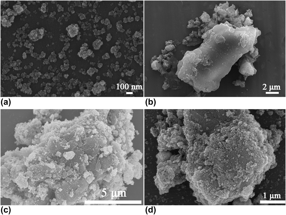
Figure 4 shows SEM images of the microstructures of the Bi2WO6, C3N4, and C3N4/Bi2WO6 photocatalysts. Compared to the smaller-sized Bi2WO6 nanoparticles, pure C3N4 displayed a sheet-like morphology. The Bi2WO6 [Fig. 4(a)] nanoparticles had various morphologies. The Bi2WO6 nanoparticles were approximately 30–50 nm, and these nanoparticles tended to aggregate, forming larger structures. As shown in Fig. 4(b), C3N4 exhibited an aggregated morphology with large lamellar structures. According to Fig. 4(c), the Bi2WO6 nanoparticles were uniformly distributed on the surface of the C3N4 lamellar structures. After 30 min of ultrasonication, the morphology of C3N4/Bi2WO6 [Fig. 4(d)] did not change in a notable manner, indicating that the small Bi2WO6 nanoparticles were firmly attached to the C3N4.
SEM images of (a) Bi2WO6, (b) C3N4, (c) 20% C3N4/Bi2WO6, and (d) 20% C3N4/Bi2WO6 after 30 min of ultrasonication.
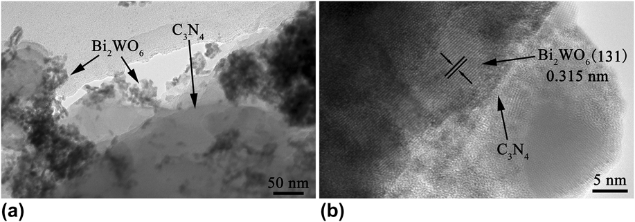
To further investigate the microstructure of C3N4/Bi2WO6, TEM was used to image the 20% C3N4/Bi2WO6 photocatalyst as shown in Fig. 5. Pure g-C3N4 consisted of sheets [Fig. 5(a)], and its surface was very smooth in agreement with the SEM images [Fig. 5(b)]. Furthermore, the Bi2WO6 nanoparticles covered the surface of the C3N4. The Bi2WO6 phase was in direct contact with C3N4, forming C3N4/Bi2WO6 heterojunctions. To better understand the structure of C3N4/Bi2WO6 heterojunction, an HRTEM image of the 20% C3N4/Bi2WO6 photocatalyst was obtained [Fig. 5(b)]. The HRTEM image revealed that the lattice spacing was approximately 0.315 nm, which was consistent with the (131) spacing of Bi2WO6.Reference Zhang, Wong, Chen, Jimmy, Zhao, Hu, Chan and Wong20 These results were in accordance with the XRD patterns shown in Fig. 1. Clearly, a heterojunction was formed between Bi2WO6 and C3N4. This heterojunction promoted charge transfer between C3N4 and Bi2WO6 and separation of photogenerated electron–hole pairs, both of which enhanced the photocatalytic activity of the material.
(a) TEM and (b) HRTEM images of 20% C3N4/Bi2WO6.
The optical absorption of the as-prepared samples was also investigated. Figure 6(a) shows the UV-vis diffuse reflectance spectra of C3N4/Bi2WO6, Bi2WO6, and C3N4. Combining C3N4 and Bi2WO6 caused a red-shift in the absorption edge, improving the absorption of light in the visible region. The visible light absorption of C3N4/Bi2WO6 also increased with increasing C3N4 content.
(a) UV-vis diffuse reflectance spectra of C3N4, Bi2WO6, and C3N4/Bi2WO6. (b) Plots of (αhν)2 versus (hν) for C3N4 and Bi2WO6.
The intercept of the tangent to the plot of (ahν)2 versus hν [Fig. 6(b)] provides a good approximation of the band gap energies of Bi2WO6, C3N4, and 20% C3N4/Bi2WO6. As shown in the figure, the absorption edge of Bi2WO6 was approximately 432 nm, which corresponded to the band gap of 2.87 eV.Reference Fu, Pan, Zhang and Zhu21–Reference Ma, Zhou, Hu, Jiang and Huang23 C3N4 had an absorption edge at 454 nm, which can be assigned to a band gap of 2.73 eV. The band gap of 20% C3N4/Bi2WO6 was 2.65 eV. Compared to Bi2WO6, the 20% C3N4/Bi2WO6 had enhanced visible-light absorption from 432 nm to 468 nm, which may have been attributed to the heterojunctions formed at the C3N4 and Bi2WO6 interfaces. This enhanced visible-light absorption strongly suggests that 20% C3N4/Bi2WO6 can absorb more visible light to produce more photogenerated electron–hole pairs, which would contribute to its VLD photocatalytic activity.
B. Photocatalytic activity
The photocatalytic activities of P25, Bi2WO6, and C3N4/Bi2WO6 toward the degradation of RhB in water were evaluated under visible-light irradiation. Figure 7 shows the normalized concentration of RhB in the system as a function of time for photocatalytic degradation under irradiation by visible light. The photolysis of RhB was negligible in the absence of the photocatalysts, indicating that RhB was stable under irradiation by visible light. Among the photocatalysts tested, 20% C3N4/Bi2WO6 exhibited the highest photocatalytic activity, and the photocatalytic degradation of RhB reached 99% within 100 min. However, when the weight ratio of C3N4/Bi2WO6 was increased from 40% to 50%, the photocatalytic activity of C3N4/Bi2WO6 was reduced and reached a lower value than that of Bi2WO6. This indicated that the weight ratio of C3N4/Bi2WO6 significantly affected the final activity of the composites. At a high C3N4 percentage, such as for 50% C3N4/Bi2WO6, the photocatalytic activity of the composite was lower than that of pure Bi2WO6, because the C3N4/Bi2WO6 interface and surface area of the heterojunction were smaller. These results suggest that an enhanced photocatalytic activity can be obtained by constructing C3N4/Bi2WO6 heterojunctions, which favor the separation of photogenerated electron–hole pairs and the transfer of charge carriers.
Photocatalytic degradation curves of RhB by Bi2WO6 and C3N4/Bi2WO6 under irradiation by visible light (λ > 420 nm).
The reaction kinetics of the degradation rate of the RhB solution was quantitatively compared under visible irradiation (λ > 420 nm). As shown in Fig. 8, the apparent rate constants, k app, of Bi2WO6 and 20% C3N4/Bi2WO6 were 0.007 and 0.0293 min−1, respectively. The photocatalytic activity of 20% C3N4/Bi2WO6 was 4.19 times that of Bi2WO6.
Apparent rate constants for the photodegradation of RhB by Bi2WO6 and C3N4/Bi2WO6 under irradiation by visible light (λ > 420 nm).
To evaluate the stability of the 20% C3N4/Bi2WO6 photocatalyst, five cycles of the photodegradation of RhB were performed (Fig. 9). The concentration of RhB decreased by 98% after 100 min during the first run. After being used four times, the catalyst did not experience a significant loss of photocatalytic activity in the fourth cycle. Variations in the XRD analysis (Fig. 10) illustrated that the crystal structure of the 20% C3N4/Bi2WO6 photocatalyst did not change after the cycling photocatalytic experiments. Therefore, the 20% C3N4/Bi2WO6 photocatalyst can be inferred as a stable photocatalyst.
Normalized RhB concentration versus time for 20% C3N4/Bi2WO6 over five cycles during photocatalytic decomposition under irradiation by visible light (λ > 420 nm).
XRD patterns of 20% C3N4/Bi2WO6 before and after the cycling photocatalytic experiments.
PL spectra are a useful tool for investigating the migration, transfer, and recombination of photogenerated electron–hole pairs in semiconductors, because PL emission mainly results from the recombination of photogenerated electron–hole pairs. Generally speaking, higher PL emission intensities correspond to higher recombination efficiencies for photogenerated electron–hole pairs and lower photocatalytic activities. Figure 11 shows the PL spectra of the different C3N4/Bi2WO6 samples. The 20% C3N4/Bi2WO6 sample displayed the lowest emission intensity, suggesting that it possessed the highest photocatalytic activity, which was in agreement with the results of the photodegradation of RhB.
PL spectra of 10, 20, 30, 40, and 50% C3N4/Bi2WO6.
The above results strongly suggest that the formation of heterojunctions by combining C3N4 and Bi2WO6 enhances VLD photocatalytic activity compared to the use of Bi2WO6 alone. Based on the experimental results, a possible mechanism of the VLD photocatalytic activity of the C3N4/Bi2WO6 heterojunction was proposed as illustrated in Fig. 12. It is believed that in the C3N4/Bi2WO6 heterojunction, the interface between C3N4 and Bi2WO6 inhibits the recombination of photogenerated electron–hole pairs. Under visible-light irradiation, C3N4 and Bi2WO6 are excited simultaneously, producing photogenerated electron–hole pairs. Based on the band gap positions, the estimated conduction band (CB) and valence band (VB) of C3N4 are −1.13 and 1.6 eV. The CB and VB edge potentials of Bi2WO6 were at 0.39 and 3.26 eV, respectively. The CB and VB edge potentials of C3N4 were more negative than that of Bi2WO6. Therefore, because the CB of C3N4 is at a higher energy level than that of Bi2WO6, electrons in the CB of C3N4 are more easily transferred to the CB of Bi2WO6 by controlling the interface. Meanwhile, the holes in the VB of Bi2WO6 can transfer to the VB of C3N4 through the interface, because the energy level of the VB of Bi2WO6 is lower than that of C3N4 (Fig. 12). The process can be described as follows:
 $${{{{\rm{C}}_3}{{\rm{N}}_4}} \mathord{\left/ {\vphantom {{{{\rm{C}}_3}{{\rm{N}}_4}} {{\rm{B}}{{\rm{i}}_2}{\rm{W}}{{\rm{O}}_6}}}} \right. \kern-\nulldelimiterspace} {{\rm{B}}{{\rm{i}}_2}{\rm{W}}{{\rm{O}}_6}}}\left( {h\nu } \right) \to {{{{\rm{C}}_3}{{\rm{N}}_4}\left( {{{\rm{e}}^ - } + {\rm{\ }}{{\rm{h}}^ + }} \right)} \mathord{\left/ {\vphantom {{{{\rm{C}}_3}{{\rm{N}}_4}\left( {{{\rm{e}}^ - } + {\rm{\ }}{{\rm{h}}^ + }} \right)} {{\rm{B}}{{\rm{i}}_2}{\rm{W}}{{\rm{O}}_6}\left( {{{\rm{e}}^ - } + {\rm{\ }}{{\rm{h}}^ + }} \right)}}} \right. \kern-\nulldelimiterspace} {{\rm{B}}{{\rm{i}}_2}{\rm{W}}{{\rm{O}}_6}\left( {{{\rm{e}}^ - } + {\rm{\ }}{{\rm{h}}^ + }} \right)}}\quad ,$$
 $${{{{\rm{C}}_3}{{\rm{N}}_4}\left( {{{\rm{e}}^ - } + {\rm{\ }}{{\rm{h}}^ + }} \right)} \mathord{\left/ {\vphantom {{{{\rm{C}}_3}{{\rm{N}}_4}\left( {{{\rm{e}}^ - } + {\rm{\ }}{{\rm{h}}^ + }} \right)} {{\rm{B}}{{\rm{i}}_2}{\rm{W}}{{\rm{O}}_6}\left( {{{\rm{e}}^ - } + {\rm{\ }}{{\rm{h}}^ + }} \right)}}} \right. \kern-\nulldelimiterspace} {{\rm{B}}{{\rm{i}}_2}{\rm{W}}{{\rm{O}}_6}\left( {{{\rm{e}}^ - } + {\rm{\ }}{{\rm{h}}^ + }} \right)}} \to {{{{\rm{C}}_3}{{\rm{N}}_4}\left( {{{\rm{h}}^ + }} \right)} \mathord{\left/ {\vphantom {{{{\rm{C}}_3}{{\rm{N}}_4}\left( {{{\rm{h}}^ + }} \right)} {{\rm{B}}{{\rm{i}}_2}{\rm{W}}{{\rm{O}}_6}}}} \right. \kern-\nulldelimiterspace} {{\rm{B}}{{\rm{i}}_2}{\rm{W}}{{\rm{O}}_6}}}\left( {{{\rm{e}}^ - }} \right)\quad .$$
Schematic diagram of the photocatalytic degradation of RhB on C3N4/Bi2WO6 under irradiation by visible light.
Meanwhile, Bi2WO6 [Fig. 4(a)] also displayed a variety of morphologies, and the diameters of the Bi2WO6 nanoparticles were approximately 30–50 nm. The larger surface area of the Bi2WO6 nanoparticles favored the ability of the photo-generated charge carrier to transfer electrons at the interface. This transference effectively suppressed the recombination of photogenerated electron–hole pairs and, therefore, resulted in an enhanced VLD photocatalytic activity. According to Fig. 7, pure Bi2WO6 possessed a higher VLD photocatalytic activity than pure C3N4. Therefore, an appropriate weight ratio of the C3N4/Bi2WO6 heterojunction must be selected to produce the most effective separation of photogenerated electron–hole pairs. When the weight ratio of C3N4/Bi2WO6 was above 20%, insufficient Bi2WO6 was available to achieve an effective separation of photogenerated electron–hole pairs. Nevertheless, the addition of too much of the relatively low-efficiency C3N4 in the heterojunction resulted in a low VLD photocatalytic activity. The optimum weight ratio was found to be 20% C3N4/Bi2WO6. In addition, as shown in the UV-vis diffuse reflectance spectra of 20% C3N4/Bi2WO6 (Fig. 6), 20% C3N4/Bi2WO6 displayed enhanced visible-light absorption from 432 nm to 468 nm compared to that of pure Bi2WO6. This enhanced visible-light absorption suggests that 20% C3N4/Bi2WO6 was able to absorb more visible light for the production of photogenerated electron–hole pairs, which contributed to its high VLD photocatalytic activity. The 20% C3N4/Bi2WO6 heterojunction exhibited the highest photocatalytic activity.
IV. CONCLUSIONS
C3N4/Bi2WO6 heterojunction photocatalysts were successfully synthesized by consecutive hydrothermal and calcination processes. SEM and TEM images indicated that the Bi2WO6 nanoparticles formed were approximately 30–50 nm, and they were uniformly distributed on the surface of C3N4 lamellar structures. The 20% C3N4/Bi2WO6 sample displayed enhanced visible-light absorption from 432 nm to 468 nm. As compared to pure Bi2WO6, 20% C3N4/Bi2WO6 exhibited approximately 4.19 times enhancement in photocatalytic activity, because the separation efficiency of the photogenerated electron–hole pairs was improved. The heterojunction formed between C3N4 and Bi2WO6 contributed to the improved separation of photogenerated electron–hole pairs and enhanced photocatalytic activity of the composite material.
ACKNOWLEDGMENT
This work was financially supported by the National Natural Science Foundation of China (NSFC Grant No. 51572245)