I. INTRODUCTION
Increasing requirements for high reliability of semiconductor devices continuously motivate improvements in device designs as well as in manufacturing equipment and processing technology to provide a robust basis for high yield and reproducibility. A growing variety of applications for detectors of ultraviolet (UV) radiation, such as relating to food, air and drinking water purification, flame and combustion control as well as chemical and biological analysis or sterilization of biological and medical equipment depend on highly reliable and long-term stable detection systems. UV photodetectors based on narrow band gap semiconductors such as silicon, gallium arsenide (GaAs), and gallium phosphide (GaP) face limitations that are inherent to their material properties. Due to the low band gap, the devices are sensitive to low-energy radiation and must be cooled for high-sensitivity applications to reduce the dark current. Exposure to UV radiation of much higher energy than the semiconductorband gap accelerates device aging.Reference Monroy, Omnes and Calle1–Reference Werner4 UV photodetectors based on wide band gap semiconductors such as silicon carbide (SiC), gallium nitride (GaN), and aluminum gallium nitride (AlGaN) enable room-temperature operation and provide intrinsic visible blindness, i.e., the detection of low UV radiation even in highly intense visible or infrared ambient light (visible blindness > 104). The higher strength of the chemical bonds enhances their radiation hardness and the higher thermal conductivity allows high-temperature and high-power applications.Reference Monroy, Omnes and Calle1, Reference Razeghi and Rogalski2
SiC-based photodetectors belong to the most efficient among semiconductor UV detectors currently available in the UV range between 200 and 380 nm. First commercial p–n junction devices were fabricated on p-type 6H–SiC substrates and exhibited very low dark current of about 10−11 A/cm2 at −1.0 V reverse bias even at a temperature of 473 K.Reference Brown, Downey, Ghezzo, Kretchmer, Saia, Liu, Edmond, Gati, Pimbley and Schneider5, Reference Edmond, Kong, Suvorov, Waltz and Carter6 Such commercial SiC photodiodes were demonstrated to be robust against nuclear radiation.Reference Metzger, Henschel, Köhn and Lennartz7 Due to the commercialization of SiC devices, reliability issues have attracted more and more attention.Reference Holz, Hultsch, Scherg and Rupp8 The development of stable ohmic contacts to SiC has been subject of extensive research.Reference Borysiewicz, Kaminska, Mysliwiec, Wzorek, Kuchuk, Barcz, Dynowska, di Forte-Poisson, Giesen and Piotrowska9–Reference Downey, Flemish, Liu, Clark and Mohney11 Also, hardness against ionizing and particle radiation has been studied in detail.Reference Cavallini, Castaldini and Nava12–Reference Moscatelli16 Robustness against UV irradiation is an important issue for UV dose control systems in germicidal and bactericidal UV applications. They call for highly reliable UV detectors to monitor the power emitted by an UV light source and require UV photodiodes that are long-term stable under UV irradiation. Recently, aging behavior of 4H–SiC Schottky photodiodes after 200 h of high-intensity mercury lamp exposure was studied.Reference Sciuto, Mazzillo, Raineri, Catania, D’Arrigo and Roccaforte17
In the present article, we describe the epitaxial growth, fabrication, and characterization of SiC p–n junction photodiodes on n-type substrates and their long-term behavior under different conditions of highly intense UV exposure. Due to its physical properties, hexagonal 4H–SiC polytype has advantage over the 6H–SiC polytype and was chosen as substrate for the photodiodes fabricated in this study. Compared with 6H–SiC, the band gap of 4H–SiC is larger (3.26 eV at 300 KReference Goldberg, Levinshtein, Rumyantsev, Levinshtein, Rumyantsev and Shur18), which shifts the peak sensitivity to a shorter UV wave length and improves the visible blindness. Higher carrier mobilities and longer diffusion lengths of 4H–SiC enable superior UV photoresponse and quantum efficiency. The peak of the external quantum efficiency of a 4H–SiC photodiode was reported to be higher by about 5% than that of a 6H–SiC photodiode.Reference Park, Kimoto and Matsunami19 In this study, 4H–SiC p–n junction photodiodes were stressed under UV irradiation emitted by a medium-pressure mercury lamp for 93 h and by a low-pressure mercury ultraviolet light C-band (UV-C, peak emission at 254 nm) lamp for a duration of 22 months.
II. EPITAXIAL GROWTH
4H–SiC epitaxial layers were grown in a commercial hot-wall chemical vapor deposition (CVD) system that was previously described in detail.Reference Wagner, Schulz and Siche20 The system does not allow for rotation of the wafer during growth. To suppress contamination with impurities the susceptor and the substrate carrier were made of high-purity graphite coated with SiC. 4H–SiC epitaxial layers were grown on commercially available n-type 4H–SiC (0001) substrates, off-oriented 4° toward < $11\overline 2 0$>, with diameters of 76 mm (SiCrystal AG; Cree, Inc., Durham, NC). Prior to loading the substrates, they were sequentially cleaned with organic solvents, hot H2SO4:H2O2 (3:1), H2O:HCl:H2O2 (6:1:1), rinsed with deionized water followed by immersion in a hydrofluoric acid (HF) solution for removing the surface oxide. Before layer deposition the reaction cell, including susceptor and substrate, was baked at 1200 °C down to a background pressure below 10−5 mbar for removing undesired background doping impurities. The epitaxial growth was performed using silane (2.5% diluted in H2) and propane (5% diluted in H2) as precursors and trimethylaluminum (TMA) as a p-type and nitrogen (N2) as n-type doping source. Palladium-purified hydrogen was used as carrier gas. The layer thicknesses for the n-type and the p-type layers were about 5 μm and 0.15 μm and the net-donor and net-acceptor concentrations were N D–N A = 8 × 10¹⁵/cm3 and N A–N D = 6 × 10¹⁸/cm3, respectively. The layers were grown at a rate of 80 nm/min.
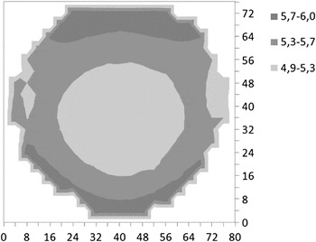
A typical thickness variation of the n-type epitaxial layers on 3-inch 4H–SiC wafers is shown in Fig. 1, measured by Fourier transform infrared (FTIR) spectroscopy. The standard deviation of a 5.5 μm thick layer is 5%. The thickness of the p-type SiC layer is extracted from ellipsometry measurements. A model that consists of differently doped SiC layers for the n–p-structure and a surface layer, which describes the surface roughness, was used to evaluate the ellipsometry data and was verified by scanning electron microscope imaging.
Thickness variation of an about 5.4 μm thick n-type 4H–SiC layer on 4H–SiC substrate with a diameter of 76 mm evaluated by FTIR spectroscopy.

N-type and p-type layers were grown in separate reaction cells to avoid an intermixing of p- and n-dopants and to obtain noncompensated layers.
III. DEVICE PROCESSING
Photodiodes were fabricated on 2- and 3-inch wafers. Modern and automated equipment has been used for dry- and wet-chemical processing, deposition of metals and dielectrics to ensure best possible process control.
Contact printing lithography using a mask aligner has been used for all patterning and alignment steps. The active area of the p–n junction diodes was defined by mesa etching using an inductively coupled plasma (ICP) with Cl2–BCl3 chemistry. Due to its chemical resistance, SiC patterning requires a sufficiently stable etch mask that was formed by SiNx. The SiNx was deposited using plasma-enhanced chemical vapor deposition (PECVD) and patterned by photolithography and ICP using sulfur hexafluoride (SF6) and oxygen (O2) chemistry. The SiC etching technology assured a high homogeneity of ±15 nm over the 3-inch wafer surface and an exact control of the total etch depth of 7 μm. The devices were passivated using wet thermal oxidation. Electrical contacts were deposited by sputtering and were patterned using lift-off. The front electrode on the p-type layer was formed by aluminum (Al)–titanium (Ti) alloy annealed at 1000 °C and a nickel (Ni)–chromium (Cr) contact was formed on the back of the n-type SiC substrate by annealing at 650–750 °C.Reference Borysiewicz, Kaminska, Mysliwiec, Wzorek, Kuchuk, Barcz, Dynowska, di Forte-Poisson, Giesen and Piotrowska9, Reference Crofton, Porter and Williams21, Reference Ohno22 Rapid thermal annealing was performed in argon atmosphere. Values of the specific contact resistance were determined by linear Transmission Line Method.Reference Crofton, Porter and Williams21 Typical values of 1 × 10⁻¹ Ω cm2 and 4 × 10⁻⁴ Ω cm2 were obtained for n-type and p-type, respectively. It should be noted, that the n-type contact resistance is about two orders of magnitude higher than the value reported in literature.Reference Crofton, Porter and Williams21 Contacts have been optimized for solderability and metal adhesion. Due to the low currents in the photodiodes in the range of about hundred nanoamps to some picoamps a relatively high specific contact resistance is not critical for device performance.
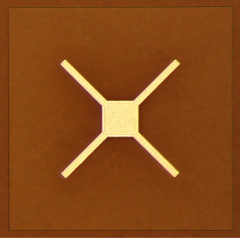
Finally, the devices were separated by wafer dicing. Different chip dimensions of up to 6 × 6 mm2 have been fabricated. Figure 2 shows the top view of a 4H–SiC p–n photodiode fabricated.
Optical micrograph of the front of a processed photodiode. The electrical contact has a bonding island in the center (bright). The edge length of the active area of the square chip is 1 mm.

IV. DEVICE CHARACTERISTICS
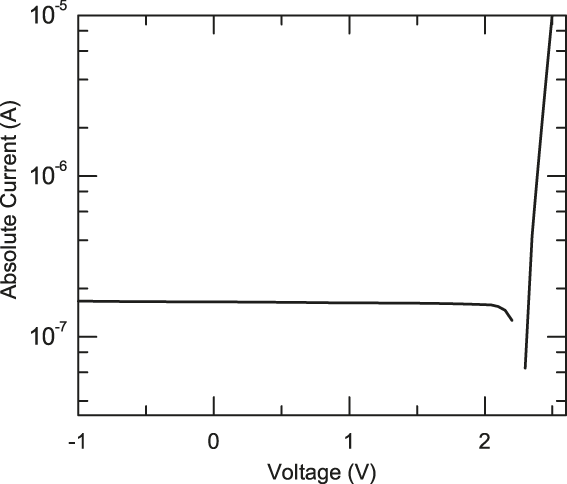
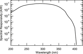
Photodiode chips packaged into a TO housing with UV transparent window were characterized at room temperature. For devices having an active area of 0.06 mm2 a dark current of 0.2 fA at 1 V reverse bias and a capacitance of 15 pF have been determined. The diodes exhibit a breakdown voltage of 125 V. Figure 3 shows typical photocurrent-voltage characteristics of the devices illuminated with an UV-C lamp (nearly monochromatic light at 254 nm) at an intensity of 4 mW/cm2. Under these conditions, a short-circuit photocurrent of 170 nA and an open-circuit voltage of 2.3 V was obtained. A 74000 Cornerstone 130 1/8 m motorized monochromator and a Newport 200 W xenon/mercury lamp type 6291 (Franklin, MA) were used to measure spectral response behavior in the wave length range of 200–450 nm. The total irradiance was monitored by a calibrated monitor diode, type Hamamatsu 5226-8BQ (Hamamatsu, Japan). Figure 4 shows the spectral response of a 4H–SiC p–n photodiode. The responsivity shows its maximum at about 300 nm and falls below 10% of maximum at wave lengths shorter than 215 nm and longer than 365 nm.
Photocurrent–voltage characteristics of a 0.06 mm² active area 4H–SiC p–n UV photodiode irradiated by nearly monochromatic 254 nm UV-C light, with intensity of 4 mW/cm2. The short-circuit photocurrent is 170 nA and the open-circuit voltage is 2.3 V.

Spectral responsivity of a typical 4H–SiC p–n UV photodiode.

Visible blindness defined as the ratio of responsivity at peak and in the visible range was tested with a 532 nm laser providing a power density of 40 mW/cm2. While irradiating a device with an active area of 1 × 1 mm2 with the green laser, no photocurrent could be detected with the used instrument (Keithley 237 SMU, Cleveland, OH) having a current measurement accuracy down to about 10. On the other hand, when illuminating with a 4 mW/cm2 low-pressure mercury UV-C lamp with a peak emission at 254 nm a photocurrent of 3.3 μA could be obtained. The visible blindness can be estimated by giving weightage and dividing these two currents to about ten orders of magnitude.
V. UV STRESSING EXPERIMENTS
To ascertain information about long-term stability of devices for UV detector applications, SiC devices were exposed to UV light for a long duration and high radiation intensity. The photodiode chips were packaged in TO18 cans with UV transparent borosilicate window material. Separate studies were conducted with low-pressure and medium-pressure mercury lamps. Both types of lamps were chosen because they are used for killing germs in air and liquids. The irradiance power of the low-pressure lamp is limited to about 4 mW/cm2. For higher irradiance power a medium-pressure lamp was used.
Long-term irradiation was performed with a low-pressure mercury UV-C lamp (Philips PL-L 36W 4P, Amsterdam, Netherlands, 4.2 mW/cm2 at peak wave length of 254 nm) for a time of 16,000 h totaling to a dose of 58 kJ/cm2. These aging experiments were performed at room temperature without temperature control or monitoring. During 22 months of irradiation stress, the devices were operated in short-circuit mode and their photocurrent was regularly measured. For short-circuit photocurrent characterization the diodes were removed from the stress setup for a short time and illuminated with a low-pressure UV-C tube (power density of about 1 mW/cm2). The photocurrents of the stressed samples were compared with the ones of three nonstressed samples.
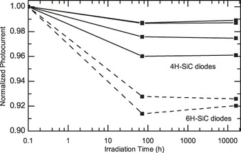
The results of the 22-months long-term stress experiment at 4.2 mW/cm2 exposure by a low-pressure UV-C lamp are shown in Fig. 5. Within the first 72 h of the irradiation the 4H–SiC p–n diodes exhibit a burn-in effect, i.e., the responsivities decrease by less than 4%. For comparison, two of the previously available 6H–SiC devices (CREE CD-260-0.30-D, on p-type SiC substrates) were tested in parallel under identical stressing conditions. Their responsivities dropped by less than 9% (see Fig. 5). After initial burn-in, for all devices no significant degradation is detectable within the accuracy of the measurement. All devices are fully functional after 16,000 h of UV irradiation and provide more than 95% of their initial photocurrent.
Normalized photocurrent of SiC UV photodiodes stressed with a low-pressure UV-C lamp. The solid lines show a burn-in effect of less than 4% within the first 72 h for 4H–SiC. The dashed lines show a burn-in effect of less than 9% within the first 72 h for 6H–SiC. After burn-in no degradation of photocurrent could be measured until now (16,000 h of irradiation).

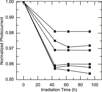
A second group of devices was irradiated by a medium pressure mercury discharge lamp (model uv-technik meyer UVH2022-17, Ortenberg, Germany). The lamp was operated at 1.8 kW constant electrical power and provided a total irradiance of 17 mW/cm2. During UV irradiation, the photodiodes were mounted to a water-cooled heat sink to minimize degradation due to elevated temperatures. More details of this setup are given elsewhere.Reference Nowy, Barton, Pape, Sperfeld, Friedrich, Winter, Hopfenmüller, Weiss, Park and Ikonen.23 The devices were exposed for 93 h totaling to a UV dose of 5.7 kJ/cm2. During exposure the devices were operated at short-circuit mode. The accelerated aging process was temporarily interrupted for photocurrent characterization with a low-pressure mercury discharge lamp (Wedeco NLR 1825, Herford, Germany). This lamp provided a total UV irradiance of about 1 mW/cm2. The characterization was done at the beginning, after 42 h, 64 h, and 93 h. The photocurrent of the stressed samples was compared with the photocurrent of two nonstressed reference samples. Again, as displayed in Fig. 6 the stressed devices exhibit a decrease of the photocurrent response of less than 5% within 93 h of exposure. This value corresponds with the ones observed in the long-term stress test under low-pressure UV-C lamp irradiation (see Fig. 5). We also note, that the photocurrent response drops mainly in the beginning of the exposure stress. All results confirm that the devices are long-term stable under high-intensity UV light irradiation and after an initial burn-in period, no significant change of the photoresponse has been detected. All stress tests are still ongoing and no failure has been detected so far. A root cause analysis for the burn-in behavior of the devices will also consider a possible influence of diode mounting and packaging materials.
Normalized photocurrent of 4H–SiC UV photodiodes stressed with a medium-pressure UV lamp. A decrease of the photocurrent of less than 5% within the first 42 h could be detected. After 42 h the photocurrent remains constant until 92 h.

VI. CONCLUSIONS
Highly efficient and reliable 4H–SiC p–n photodiodes have been fabricated on n-type substrates with active areas of up to 6 × 6 mm2. Electrical and optical characteristics of the devices were measured before and after artificial aging under high-intensity UV irradiation for up to 22 months. An initial burn-in effect was observed after 40 h, which is manifested in a drop of the photocurrent response by less than 5%. UV stress tests with previously available 6H–SiC p–n photodetectors fabricated on p-type substrates also exhibited a burn-in behavior. After initial burn-in no measurable degradation was detected. The aging tests confirm that the 4H–SiC p-on-n photodiodes are robust and suitable for high irradiance UV applications.
ACKNOWLEDGMENTS
This work was supported in part by the Federal Ministry for Economy and Technology based on decision of the German Parliament under Grant No. KF2194501DB9 and KF2303704RR9. Part of the work was funded by the Transfer BONUS program of Berlin’s Senate Department for Economy, Technology and Women. The authors also wish to thank Frank Kudella, Andreas Braun, Oliver Hilt and George Brandes for technological support and Nicolas Hübener for administrative assistance.