Introduction
With the development of microwave wireless communication system, the demand for reconfigurable bandpass filters (BPFs) [Reference Tu and Chang1–Reference Simpson, Roberto and Psychogiou24] has increased rapidly. And over the years, tunable filters play an even more important role in cognitive radio and radar applications due to compact size and cost reduction. Many methods can be applied to implement tunable filters, such as piezoelectric transducers [Reference Tu and Chang1], ferroelectric devices [Reference Zheng, Sazegar, Maune, Zhou, Binder and Jakoby2], microelectromechanical systems (MEMS) [Reference Huang, Fouladi and Mansour3, Reference Park, Lee and Rebeiz4], and varactor diodes [Reference Tang and Hong5–Reference Chen17]. Among them, varactor diodes have been widely used in the design of tunable filters, owing to flexibly tunability, compact size, low cost, and high tuning speed. Single-band tunable BPFs are proposed in [Reference Tang and Hong5–Reference Athukorala and Budimir7]. A tunable BPF is realized in [Reference Chen, Ma, Cai, Zhou, Bao and Che6] with harmonic suppression, but it suffers from limited frequency tuning range. Recently, BPFs with dual-band tunable characteristic can be achieved in [Reference Chaudhary, Choi, Jeong, Lim, Kim and Kim8–Reference Pal, Mandal and Dwari16]. However, many features within these proposed tunable dual-band BPFs (TD-BPFs) are not so ideal. For example, only one of two passbands can be tuned in [Reference Chaudhary, Choi, Jeong, Lim, Kim and Kim8], center frequencies (CFs) of two passbands with independent tunability needs further improvement in [Reference Chaudhary, Jeong and Lim9], and the out-of-band rejection of the tunable BPF is insufficient in [Reference Chen and Chu10]. Although the TD-BPFs are comprehensively reported by recent works, as far as we acknowledged, few works have focused on tunable tri-band BPF (TT-BPF) and tunable quad-band BPF (TQ-BPF).
Since the switchable filters have many advantages of multifunction and compact size, they have attracted much attention [Reference Lui, Wei and Shi18, Reference Chuang and Wu19]. PIN diodes have been introduced in [Reference Lui, Wei and Shi18], and only one of two passbands can be tuned on and off. However, in [Reference Chuang and Wu19], both the passbands can be switched on/off, so it has four possible operating states. Nevertheless, the number of operating modes mentioned above is still limited. Moreover, the above filters based on switchability are difficult to achieve tunability.
Therefore, both tunability and switchability are critical for complex reduction of communication systems. However, a few of reported BPFs can be tuned and switched simultaneously [Reference Kumar and Singh20, Reference Lu, Tang, Barker and Feng21]. The proposed BPF in [Reference Kumar and Singh20] with tunability and switchability is limited for single-band application. Stepped-impedance resonators (SIRs) are utilized in [Reference Lu, Tang, Barker and Feng21] to implement switchable single-/dual-band tunable filters. However, the out-of-band attenuation needs further improvement.
In this paper, a tunable dual-mode resonator (TDR) is proposed to achieve multi-band independent tunable and switchable BPFs. And the proposed structure can be applied to construct dual-band and tri-band tunable BPFs. Thanks to multi transmission zeros (TZs) are generated, the desired band–band isolation and high harmonic suppression can be realized. In the designed TD-BPF, the measurement results agree well with the simulation results. And the measurement results indicate that the CF of the first passband varies from 1.37 to 1.62 GHz and the CF of the second passband varies from 2.3 to 2.64 GHz. For the measured results of TT-BPF, the tuning ranges of CFs of three passbands are 1.3–1.5 GHz, 2.36–2.6 GHz, and 3–3.54 GHz, respectively. And the stopband with attenuation level of 24 dB can reach 4.6f 0, in which f 0 is the CF of the first passband. The measured results of TD-BPF and TT-BPF validate the effectiveness of the proposed methodology. For the simulation results of TQ-BPF, the tuning ranges of CFs of four passbands are 0.94–1.06 GHz, 1.66–1.98 GHz, 2.26–2.82 GHz, and 3.16–3.54 GHz, respectively.
TD-BPF analysis and design
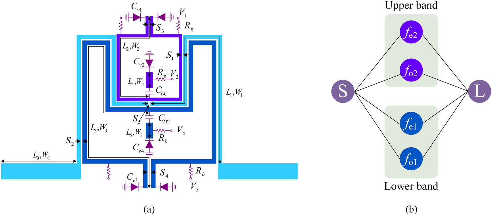
In this section, a TD-BPF is proposed and designed. As shown in Fig. 1(a), common input/output lines are utilized for two TDRs. Each TDR comprises a dual-mode open stub loaded resonator and three varactor diodes. The coupling path of the presented TD-BPF is indicated in Fig. 1(b). For the TD-BPF, four resonant modes can be excited, fo 1 and fo 2 denote the odd-mode resonant frequencies, fe 1 and fe 2 are even-mode resonant frequencies. Since the resonant frequencies can be changed by varying three capacitances of varactors simultaneously, two passbands can be independently tuned.
Proposed TD-BPF. (a) Physical layout. (b) Coupling routing diagram.

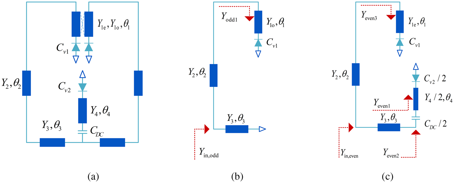
The presented TD-BPF consists of two TDRs. As indicated in Fig. 2(a), the proposed TDR comprises a transmission line with two varactor diodes Cv 1 and an open stub which is attached to a varactor diode Cv 2. And a DC block capacitor CDC is embedded at the center of the resonator. The electrical lengths and characteristic admittances of the ideal transmission line model (TLM) are respectively denoted by θi and Yi, i = 1, 2, 3, 4. Due to the symmetry of the structure, the classical odd-even mode analysis method can be utilized to obtain the resonant modes. The odd-mode and even-mode equivalent circuits are depicted in Figs 2(b) and 2(c), respectively.
Proposed TDR. (a) Transmission line model. (b) Odd-mode equivalent circuit. (c) Even-mode equivalent circuit.

The odd-mode input admittance is given by


where f denotes the reference frequency. When the resonant condition Im(Yin, odd) = 0 is satisfied, the odd-mode resonant frequency (fodd) can be derived. It can be observed from equations (1) and (2) that fodd can be changed by varying Cv 1, while fodd keeps unchanged by varying Cv 2.
The even-mode input admittance Yin, even is given by


where f denotes the reference frequency. From the resonant condition of Im(Yin, even) = 0, the even-mode resonant frequency (feven) is extracted by calculating (3)–(6). It is obvious that the change in the capacitances of Cv 1 and Cv 2 can vary the even-mode resonant frequency.
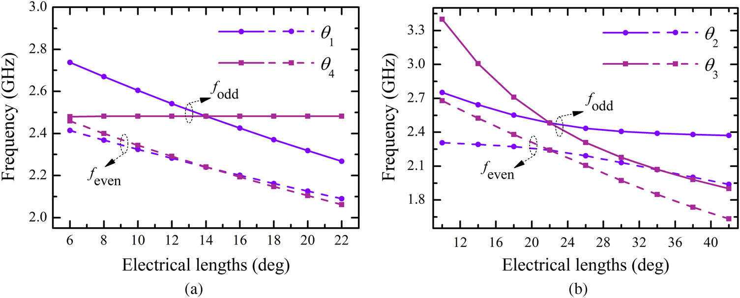
For simplicity, θ 1 = θ 4 = 14°, θ 2 = θ 3 = 22°, and Y 1e = Y 1o = Y 2 = Y 3 = Y 4/2 = 0.01 S are assumed. Meanwhile, the reference frequency f 0 is set to 2.3 GHz for electrical length calculation. To discuss the influence of the electrical lengths of the TDR on the resonant frequencies, Fig. 3 gives the resonant frequencies versus various values of θ 1, θ 2, θ 3, and θ 4. As shown in Fig. 3(a), both fodd and feven increase as θ 1 decreases, and feven decreases as θ 4 increases, while fodd keeps unchanged as θ 4 varies. In addition, fodd and feven shift down simultaneously with the increase of θ 2 and θ 3, in Fig. 3(b).
The resonant frequencies versus the various values of (a) θ 1 and θ 4. (b) θ 2 and θ 3.

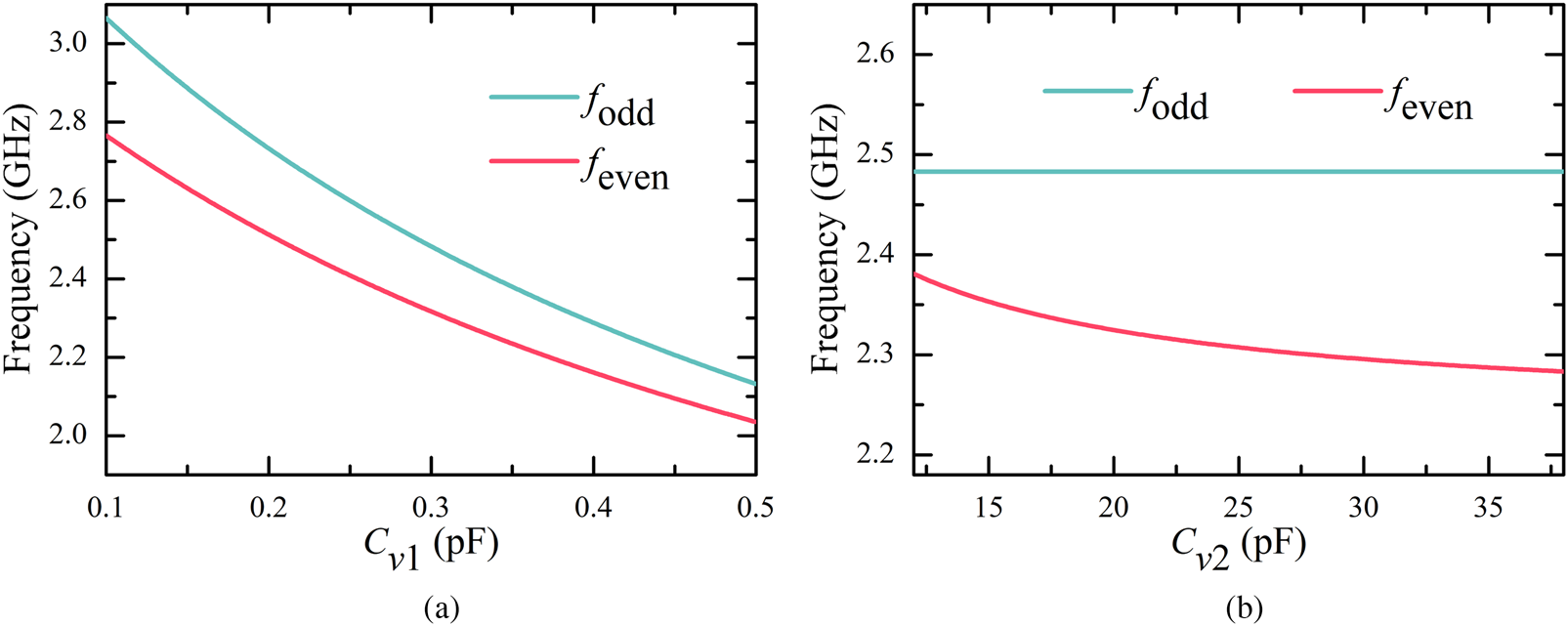
The resonant frequencies can be obtained by calculating (1)–(6). The resonant frequencies fodd and feven versus Cv 1 and Cv 2 are shown in Figs 4(a) and 4(b). As Cv 1 increases, the odd- and even-mode resonant frequencies decrease simultaneously. As Cv 2 decreases, feven shifts up while fodd keeps nearly unchanged. Therefore, by varying Cv 2, feven can be tuned independently without affecting fodd. The above characteristics of the presented structure can be used in the design of tunable passband CFs.
The resonant frequencies versus the variation of the loaded varactors. (a) Only Cv 1 varied (Cv 2 is fixed at 22 pF). (b) Only Cv 2 varied (Cv 1 is fixed at 0.3 pF).

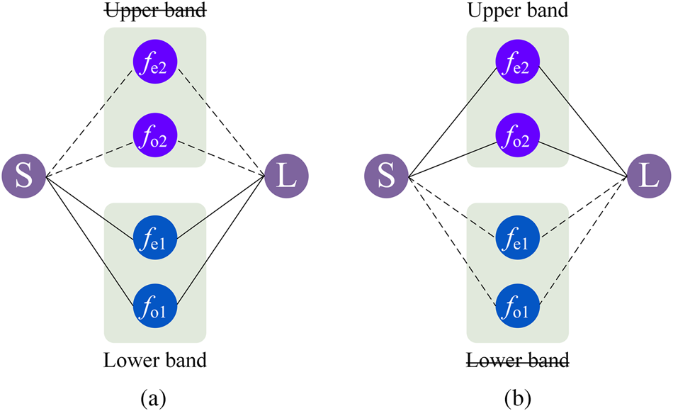
The coupling routing diagrams of the switchable TDR are presented in Fig. 5. Two coupling paths with TDRs constitute two switchable passbands. As indicated in Figs 5(a) and 5(b), when the TD-BPF works as a single-band BPF, either only the lower or the upper passband can be chosen.
Coupling routing diagrams of the switchable characteristics.(a) Single-lower band operation. (b) Single-upper band operation.

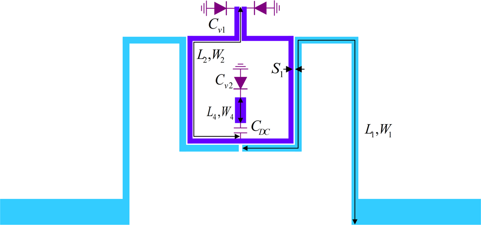
For demonstration, a TDR with feeding scheme is sketched in Fig. 6, where the S-L coupling is neglected since its effect on the external quality factor Qe is slight. The Qe of the presented TDR can be derived from the group delay of the odd-/even-modes, which can be written as


where Qexo and Qexe denote the extracted Qe of odd and even modes, respectively. $\tau _{S11\_odd/even}$ are the group delay of odd-/even-modes.
Feeding scheme of the proposed TDR.

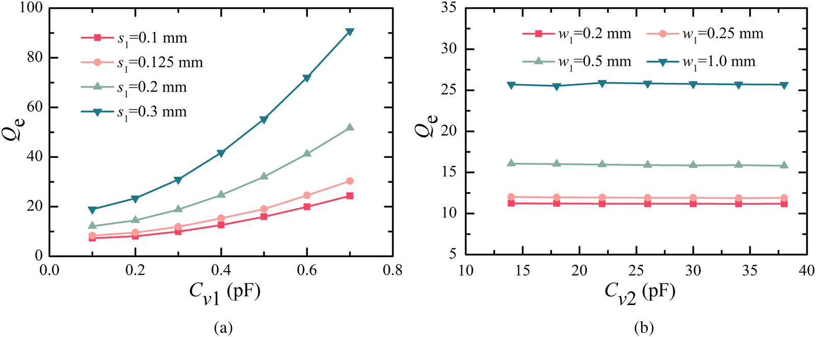
Figure 7 provides Qe versus the variation of varactor diodes with different values of s 1 and w 1. It can be found from Figs 7(a) and 7(b) that the value of Qe increases with enlargement of s 1 and w 1. And by increasing s 1, the effect of Cv 1 on Qe is obvious in Fig. 7(a). However, it has almost no influence on Qe with the variation of Cv 2 in Fig. 7(b). To fulfill the bandpass characteristic, the external quality factors should be properly selected at the varied operating frequency. Accordingly, after optimization of full-wave electromagnetic (EM) simulation, the dimension parameters in Fig. 6 can be obtained as follows: s 1 = 0.1 mm and w 1 = 0.25 mm.
External quality factor variation. (a) Qe versus Cv 1 for different values of s 1. (b) Qe versus Cv 2 for different values of w 1 (The parameters s 1 = 0.1 mm, w 1 = 0.25 mm are presented respectively. When one parameter is changed, the other keeps unchanged.).

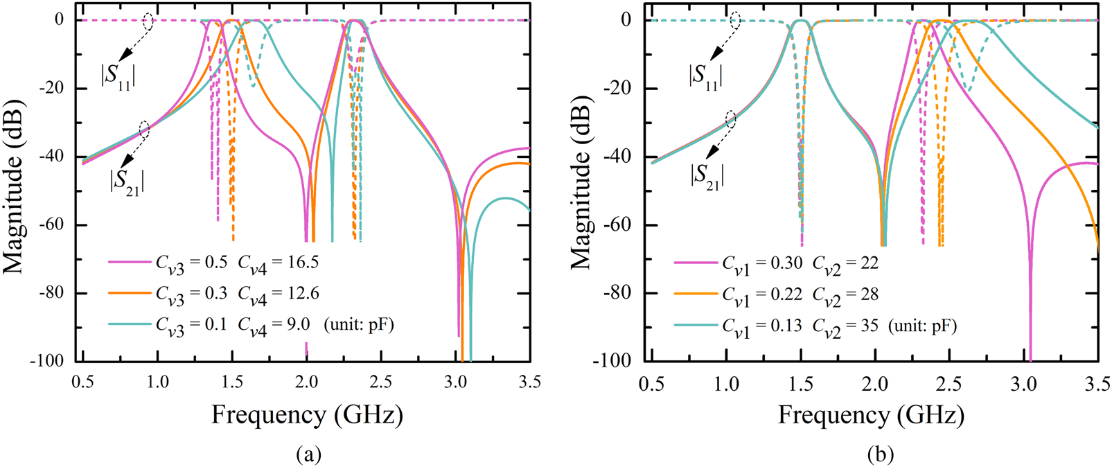
In order to obtain the desired resonant frequencies and the ideal external quality factors. As illustrated in Fig. 1(a), the optimized parameters of the proposed TD-BPF are L 0 = 5, L 1 = 21.425, L 2 = 13.5, L 3 = 25.625, L 4 = 2.1, L 5 = 1.55, W 0 = 1.15, W 1 = 0.25, W 2 = 0.2, W 3 = 0.45, W 4 = 0.7, W 5 = 0.4, S 1 = 0.1, S 2 = 0.175, S 3 = 0.1, S 4 = 0.15, S 5 = 0.1 (unit: mm). To achieve the desired tuning response, the resonant frequencies fodd and feven should be varied proportionally. Therefore, the CF of lower passband varies from 1.37 to 1.62 GHz by changing Cv 3 from 0.5 to 0.1 pF and Cv 4 from 16.5 to 9 pF, the CF of upper passband varies from 2.3 to 2.64 GHz by changing Cv 1 from 0.3 to 0.13 pF and Cv 2 from 22 to 35 pF.
TD-BPF simulation and measurement
The TD-BPF is fabricated and measured in this section. As seen in Fig. 1(a), the upper TDR is designed for a higher passband, while the lower TDR is designed for a lower passband. The fabricated TD-BPF are compact with an overall size of approximately 0.079 λg × 0.105 λg, in which λg is the guided wavelength at 1.37 GHz. The substrate of Rogers4003C made by the Rogers Corporation with a dielectric constant of 3.55, a loss tangent of 0.0027, and a substrate thickness of 0.508 mm is employed to implement the proposed TD-BPF. The measurement results are characterized by Agilent E5071C vector network analyzer.
The varactor diode MA46H120 (0.1–0.9 pF over 12 V bias, series resistance (Rs)~0.88 Ω) is selected for tuning Cv 1 and Cv 3, and the varactor diode SMV1251-079 (2.79–53.65 pF over 8 V bias, Rs~1.4 Ω) is chosen for tuning Cv 2 and Cv 4. The capacitor CDC = 33 pF is attached at the center of TDR for DC blocking purpose. The resistance Rb = 100 kΩ is embedded in the bias network to restrict the RF leakage.
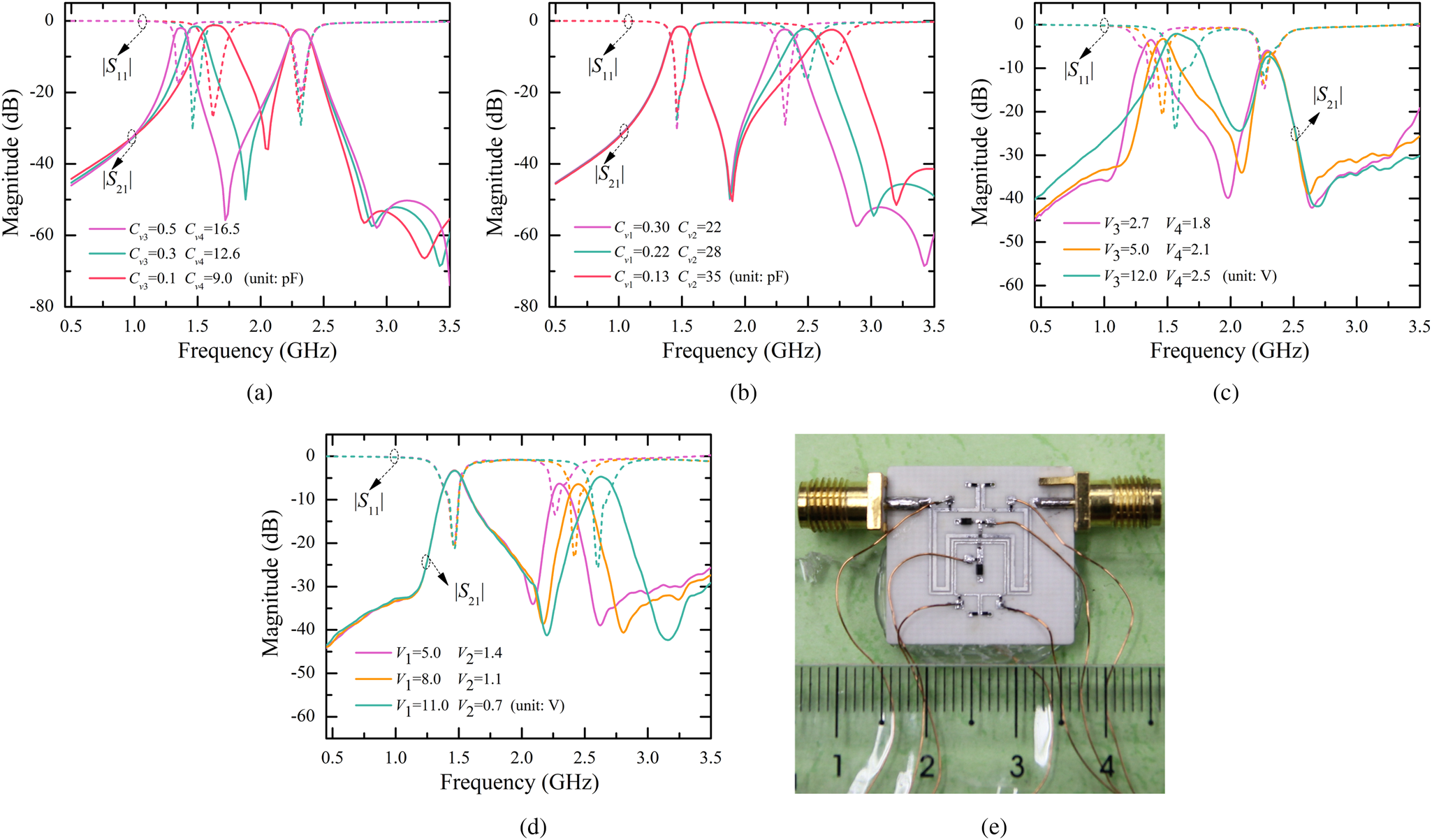
By using the ideal TLM, the S-parameters responses of the TD-BPF are simulated and portrayed in Figs 8(a) and 8(b). In addition, Figs 9(a) and 9(b) depict the full-wave EM simulated results of the presented TD-BPF. After fabrication, the measurement results of the TD-BPF is indicated in Figs 9(c) and (d), and Fig. 9(e) presents the photograph of TD-BPF. It can be seen from figures that the measurement results of the TD-BPF agree well with simulation ones. As indicated in Fig. 9(c), when V 3 is adjusted from 2.7 to 12 V and V 4 is changed from 1.8 to 2.5 V, V 1 is fixed at 5 V and V 2 is fixed at 1.4 V, the CF of the first passband is varied from 1.37 to 1.62 GHz while the CF of the second passband is fixed at 2.3 GHz. As depicted in Fig. 9(d), by keeping V 3 at 5 V and V 4 at 2.1 V, while adjusting V 1 from 5 to 11 V and V 2 from 1.4 to 0.7 V, the CF of the first passband is fixed at 1.47 GHz and the CF of the second passband is varied from 2.3 to 2.64 GHz. The return losses (RLs) are better than 11 dB in the tuning range of both passbands. The insertion losses (ILs) of the first passband (1.37–1.62 GHz) and the second passband (2.3–2.64 GHz) vary from 2 to 3.4 dB, and from 4.7 to 6.3 dB, respectively. The larger ILs are mainly caused by the circuit mismatch due to the change of the center frequency, the low value of Q of the varactors and a large number of varactors.
Simulated results of the TD-BPF using the ideal TLM. (a) The tunable first passband with fixed second passband (Cv 1 = 0.3 pF and Cv 2 = 22 pF). (b) The tunable second passband with fixed first passband (Cv 3 = 0.3 pF and Cv 4 = 12.6 pF).

Simulated and measured results of the TD-BPF. (a) The full-wave EM simulated results with tunable first passband and fixed second passband (Cv 1 = 0.3 pF and Cv 2 = 22 pF). (b) The full-wave EM simulated results with tunable second passband and fixed first passband (Cv 3 = 0.3 pF and Cv 4 = 12.6 pF). (c) The measured results with tunable first passband and fixed second passband (V 1 = 5 V and V 2 = 1.4 V). (d) The measured results with tunable second passband and fixed first passband (V 3 = 5 V and V 4 = 2.1 V). (e) The photograph of fabricated TD-BPF.

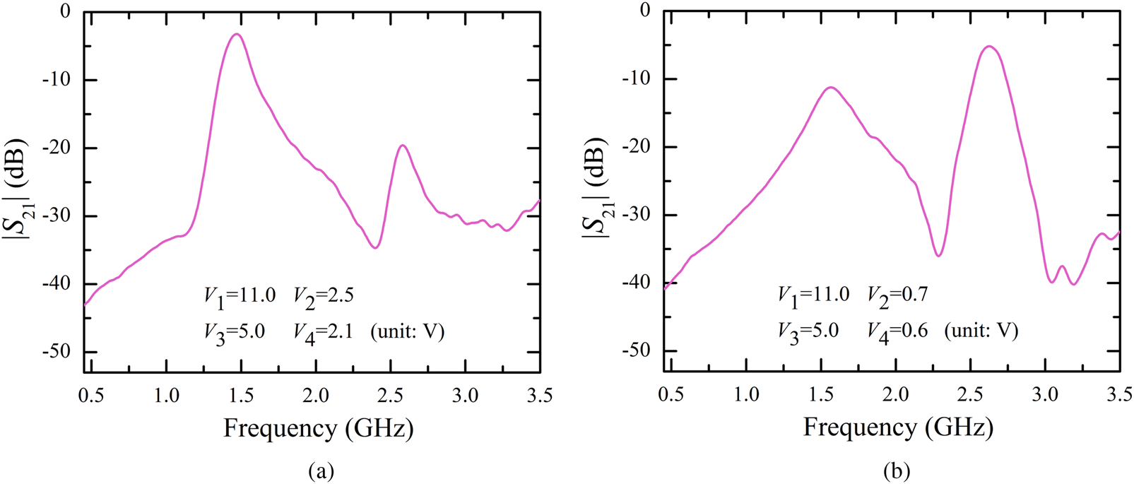
Figures 10(a) and 10(b) demonstrate the measured results of the switchable characteristics of the presented TD-BPF. By changing the voltage imposed on the varactor diode Cv 2, the second passband is turned off while the first passband remains unchanged. Vice versa, the first passband can be turned off and the second passband keeps unchanged by varying the voltage imposed on the varactor diode Cv 4. Furthermore, the passband-OFF state is owing to the passband detuning caused by the impedance mismatch of the resonator.
Measured S-parameters responses of switchable characteristics. (a) Single-lower band operation. (b) Single-upper band operation.

TT-BPF design and measurement
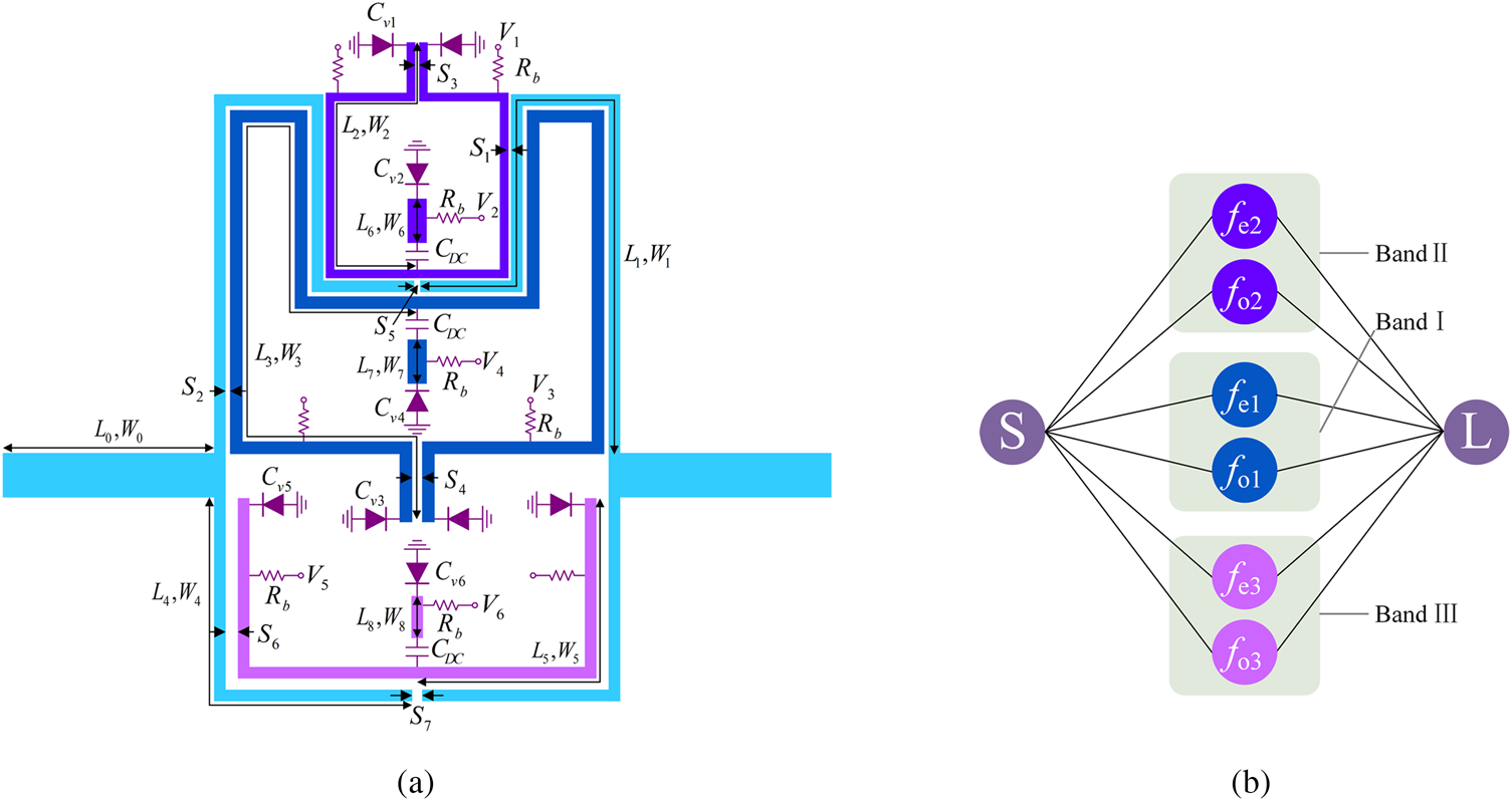
A TT-BPF is designed and measured in this section. Based on the proposed TD-BPF, two additional poles are introduced by adding a TDR. Figure 11(a) shows a layout of the proposed TT-BPF. And the coupling routing diagram of the presented TT-BPF is indicated in Fig. 11(b).
Proposed TT-BPF. (a) Physical layout. (b) Coupling routing diagram.

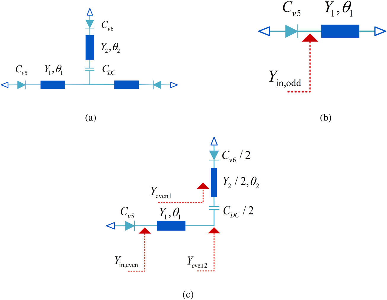
The transmission line model of the TDR is portrayed in Fig. 12(a). Two identical varactors Cv 5 attached at the end of the transmission line, and a DC block capacitor CDC is embedded at the center of the resonator. An open stub is connected at the center of the resonator with a varactor diode Cv 6. Similarly, the TDR can be analyzed by using the classical odd-even mode analysis method due to its symmetrical structure. As shown in Fig. 12, θi (i = 1, 2) and Yi (i = 1, 2) represent the electrical lengths and characteristic admittances of the ideal TLM, respectively. From Fig. 12(b), the input admittance of the odd-mode can be written as

where f denotes the reference frequency. For example, under the resonant condition Im(Yin, odd) = 0, the odd-mode resonant frequency fodd can be obtained.
Proposed TDR. (a) Transmission line model. (b) Odd-mode equivalent circuit. (c) Even-mode equivalent circuit.

From Fig. 12(c), the input admittance of the even-mode can be written as


where f denotes the reference frequency. From the resonant condition of Im(Yin, even) = 0, the even-mode resonant frequency feven is extracted by calculating (10)–(12).
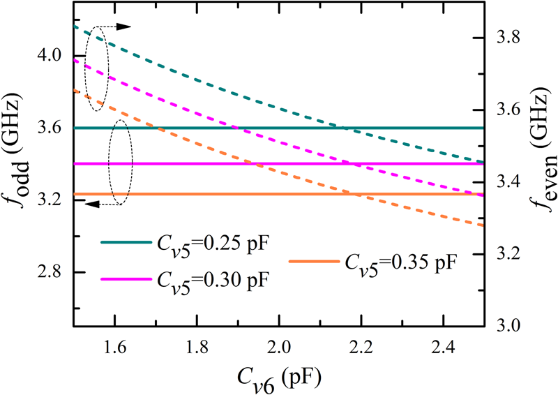
Figure 13 shows the numerical solutions of fodd and feven versus Cv 5 and Cv 6, respectively. It can be found that fodd is influenced by Cv 5, while feven is affected by both Cv 5 and Cv 6. Furthermore, feven shifts down as Cv 6 increases. And as Cv 5 decreases, both fodd and feven shift up. When Cv 5 and Cv 6 are varied proportionally, those two resonant frequencies can be tuned to lower or higher frequencies simultaneously. Therefore, the desired RL and IL can be achieved by properly tuning the Cv 5 and Cv 6.
The resonant frequencies against the values of the loaded varactors Cv 5 and Cv 6.

The substrate of the TT-BPF is the same as the TD-BPF. As seen in Fig. 11(a), the optimized dimensions of the TT-BPF are as follows: L 0 = 5, L 1 = 21.075, L 2 = 13.2, L 3 = 27.2, L 4 = 10.6, L 5 = 9.45, L 6 = 1.25, L 7 = 1.5, L 8 = 1.95, W 0 = 1.15, W 1 = 0.25, W 2 = 0.3, W 3 = 0.45, W 4 = 0.25, W 5 = 0.25, W 6 = 0.7, W 7 = 0.4, W 8 = 0.25, S 1 = 0.1, S 2 = 0.175, S 3 = 0.1, S 4 = 0.15, S 5 = 0.1, S 6 = 0.45, S 7 = 0.3 (unit: mm). The overall circuit size is approximately 0.075 λg × 0.120 λg, in which λg is the guided wavelength at 1.3 GHz. The varactor diode MA46H120 (0.1–0.9 pF over 12 V bias, Rs~0.88 Ω) is selected for Cv 1, Cv 3, and Cv 5, the varactor diode MA46H204-1056 (2–25 pF over 20 V bias, Rs~1.25 Ω) is chosen for Cv 2. Moreover, the varactor diodes SMV1251-079 (2.79–53.65 pF over 8 V bias, Rs~1.4 Ω) and SMV1233-079 (0.84–5.08 pF over 15 V bias, Rs~1.2 Ω) are used for Cv 4 and Cv 6, respectively. In addition, three 33 pF capacitors are introduced for blocking purposes. And the resistance Rb = 100 kΩ is attached to the bias network to restrict the RF leakage. The measurement results are characterized by Agilent E5071C vector network analyzer.
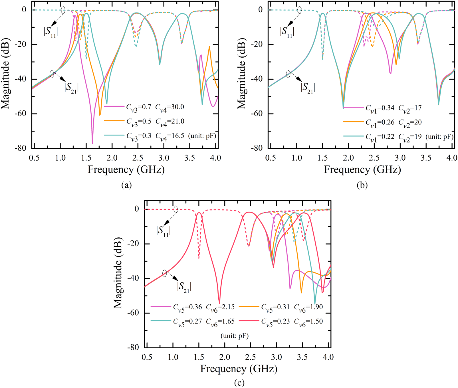
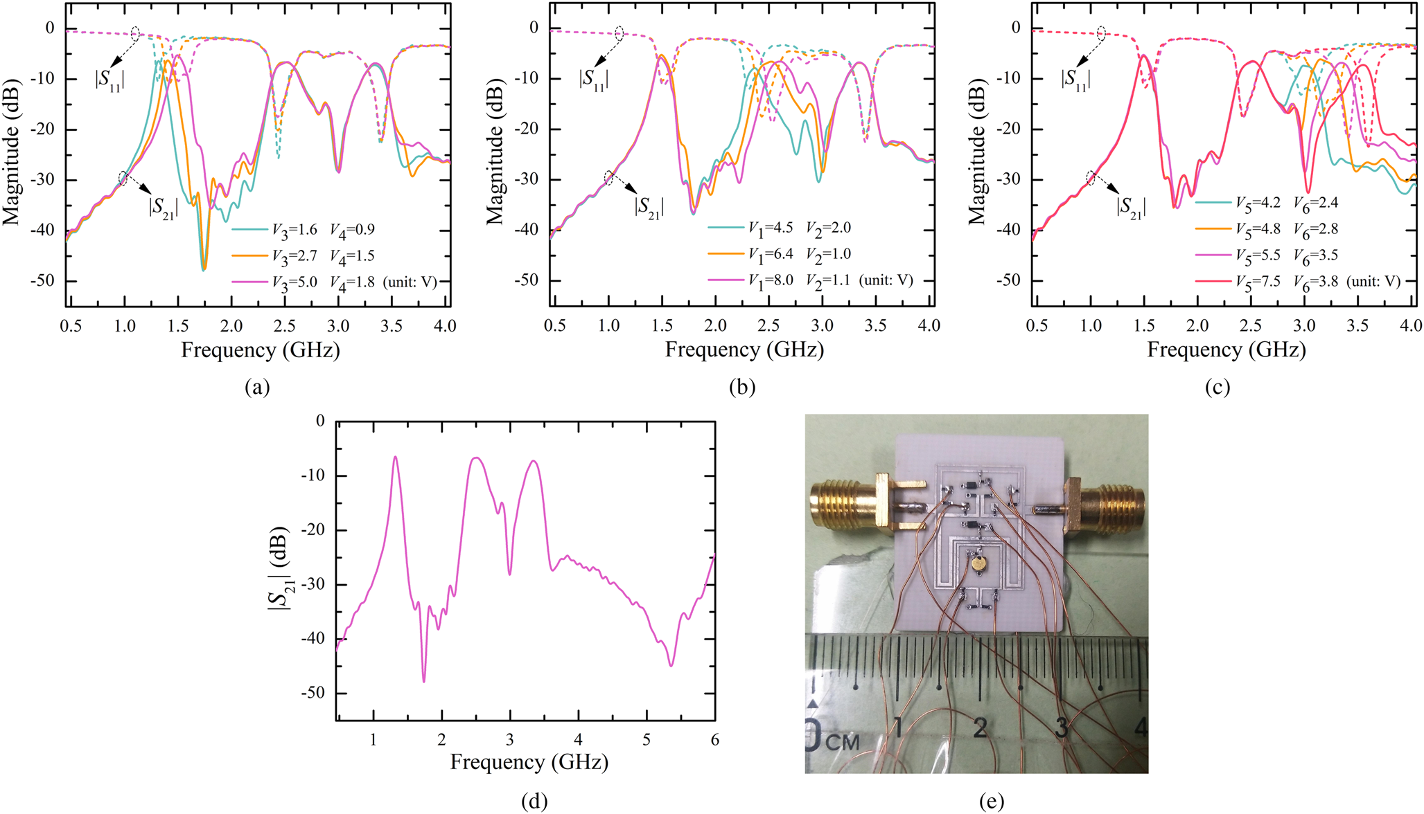
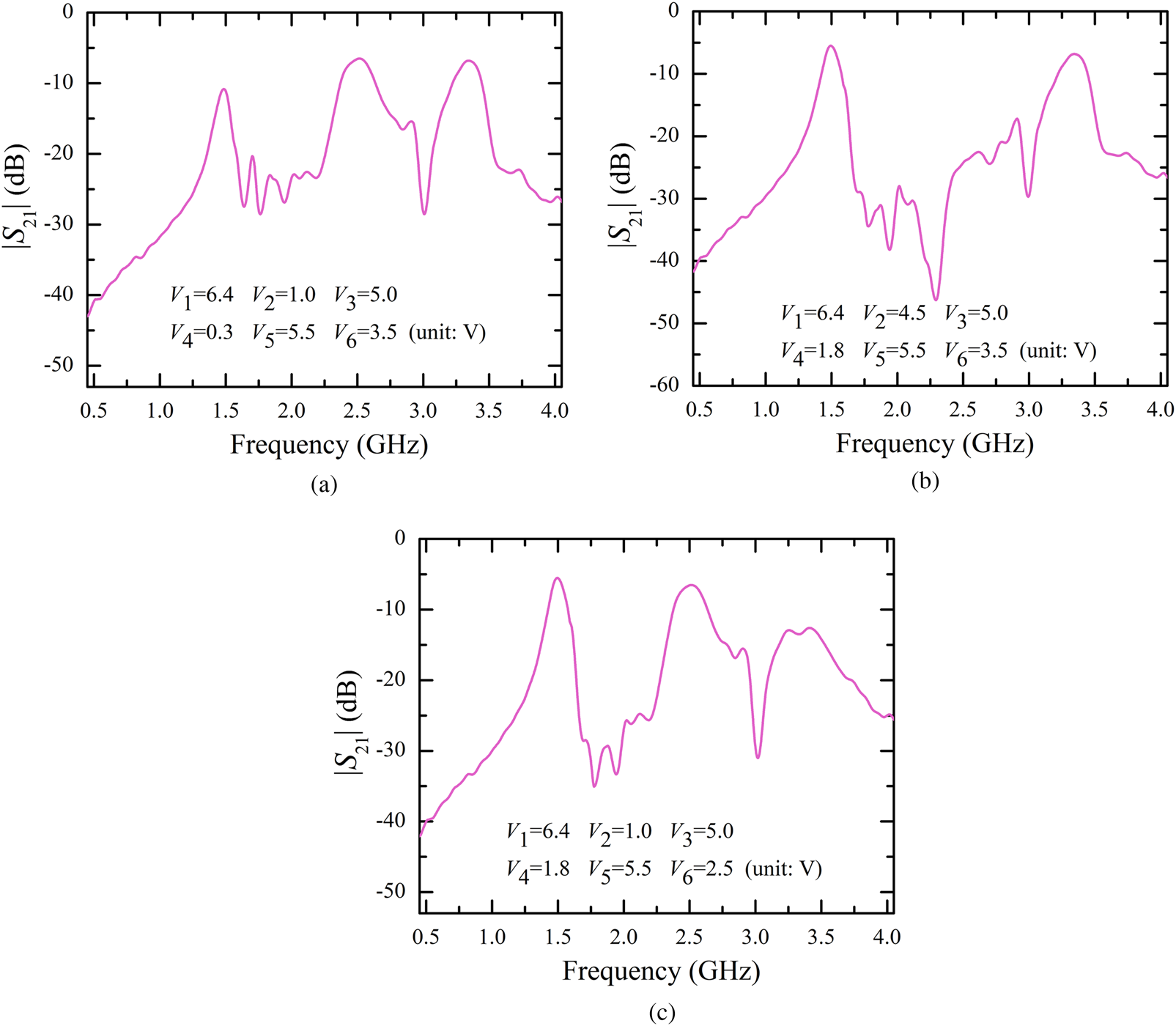
Figures 14(a)–14(c) present full-wave EM simulated results of the proposed TT-BPF. And the TT-BPF is fabricated and measured, the measured results of the TT-BPF are depicted in Figs 15(a), (b), (c), and (d), and Fig. 15(e) demonstrates the photograph of TT-BPF. We can see from the figures that the measured results of the TT-BPF are in good agreement with simulated ones. Figures 15(a)–15(c) demonstrate that the RLs are better than 10 dB over the entire tuning range of all the passbands. The first passband CF is tuned from 1.3 to 1.5 GHz with the IL varying from 5.2 to 6.4 dB, the second passband CF is tuned from 2.36 to 2.6 GHz with the IL varying from 6.6 to 7.8 dB, and the third passband CF is tuned from 3 to 3.54 GHz with the IL varying from 6.2 to 7.4 dB. It can be seen from Fig. 15 that multi TZs are generated in each sideband of passbands, which can improve band–band isolation and harmonic rejection. As seen in Fig. 15(d), the harmonic suppression with a rejection level of 24 dB can reach 4.6f 0, in which f 0 is located at 1.3 GHz. Figures 16(a)–16(c) show the measured responses of the first passband-OFF state, the second passband-OFF state and the third passband-OFF state, verifying the switchability of the designed structure. As indicated in Fig. 16(a), by adjusting V 4, the first passband is turned off. As depicted in Fig. 16(b), by changing V 2, the second passband is turned off. And as shown in Fig. 16(c), by varying V 6, the third passband is turned off.
Full-wave EM simulated results of the proposed TT-BPF. (a) The tunable first passband with fixed second and third passbands (Cv 1 = 0.26 pF, Cv 2 = 20 pF, Cv 5 = 0.27 pF and Cv 6 = 1.65 pF). (b) The tunable second passband with fixed first and third passbands (Cv 3 = 0.3 pF, Cv 4 = 16.5 pF, Cv 5 = 0.27 pF and Cv 6 = 1.65 pF). (c) The tunable third passband with fixed first and second passbands (Cv 1 = 0.26 pF, Cv 2 = 20 pF, Cv 3 = 0.3 pF, and Cv 4 = 16.5 pF).

Measured results of the proposed TT-BPF. (a) The tunable first passband with fixed second and third passbands (V 1 = 6.4 V, V 2 = 1 V, V 5 = 5.5 V, and V 6 = 3.5 V). (b) The tunable second passband with fixed first and third passbands (V 3 = 5 V, V 4 = 1.8 V, V 5 = 5.5 V, and V 6 = 3.5 V). (c) The tunable third passband with fixed first and second passbands (V 1 = 6.4 V, V 2 = 1 V, V 3 = 5 V, and V 4 = 1.8 V). (d) Harmonic suppression characteristic. (e) The photograph of fabricated TT-BPF.

Measured S-parameters responses of switchable characteristics. (a) The first passband turns off. (b) The second passband turns off. (c) The third passband turns off.

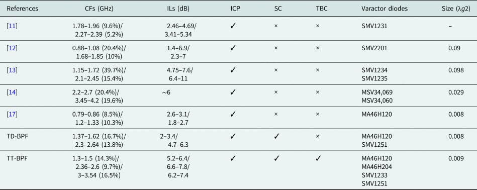
Performance comparisons of this work with several published works are listed in Table 1. The proposed BPFs can provide multi-band with tunable CFs and switchable characteristics. Further, both the presented tunable BPFs possess the merits of independent controllable passbands and compact sizes. Moreover, as far as we acknowledged, few research works have focused on achieving a tunable tri-band switchable BPF.
Comparison between this works and previous tunable BPFs.

✓, Yes; ×, No; ICP, independently controllable passbands; SC, has switchable characteristic; TBC, has tri-band bandpass characteristic.
Design of a TQ-BPF
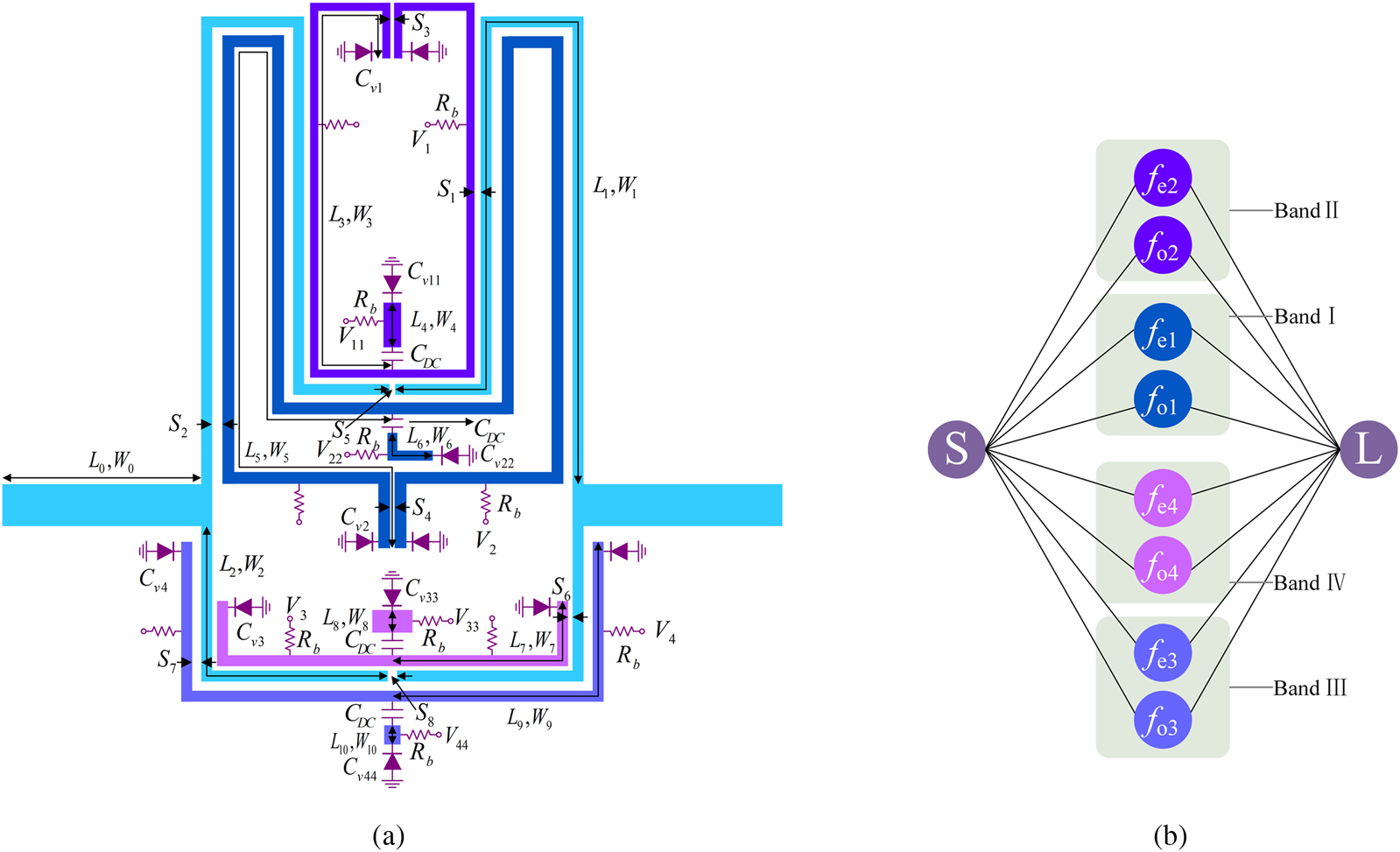
In this section, the design and simulation of the TQ-BPF are presented. Based on the proposed TT-BPF, by introducing a TDR, a TQ-BPF can be implemented. The layout and the coupling routing diagram of the TQ-BPF are depicted in Figs 17(a) and 17(b).
Proposed TQ-BPF. (a) Physical layout. (b) Coupling routing diagram.

The substrate of the TQ-BPF is the same as the above BPFs. As shown in Fig. 17(a), the physical parameters are optimized by using full-wave EM simulation, the size are L 0 = 5, L 1 = 37.3, L 2 = 12.05, L 3 = 20.07, L 4 = 2.1, L 5 = 42.9, L 6 = 2, L 7 = 7.425, L 8 = 0.65, L 9 = 12.725, L 10 = 0.4,W 0 = 1.15, W 1 = 0.35, W 2 = 0.35, W 3 = 0.35, W 4 = 0.65, W 5 = 0.475, W 6 = 0.25, W 7 = 0.2, W 8 = 1, W 9 = 0.4, W 10 = 0.35, S 1 = 0.35, S 2 = 0.5, S 3 = 0.1, S 4 = 0.1, S 5 = 0.1, S 6 = 0.15, S 7 = 0.4, S 8 = 0.15 (unit: mm). The overall circuit size is approximately 0.08 λg × 0.13 λg, in which λg is the guided wavelength at 0.94 GHz. In addition, the 100 kΩ resistors are used for preventing the RF leakage. And the 150 pF capacitors are introduced for DC blocking purpose.
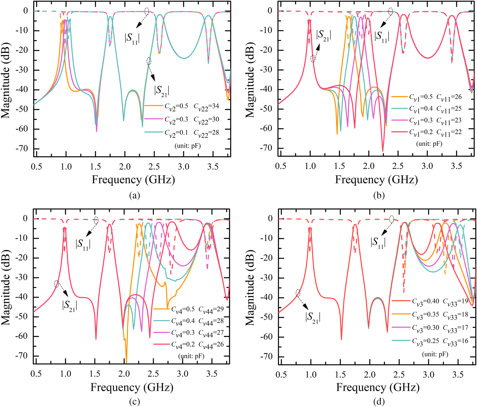
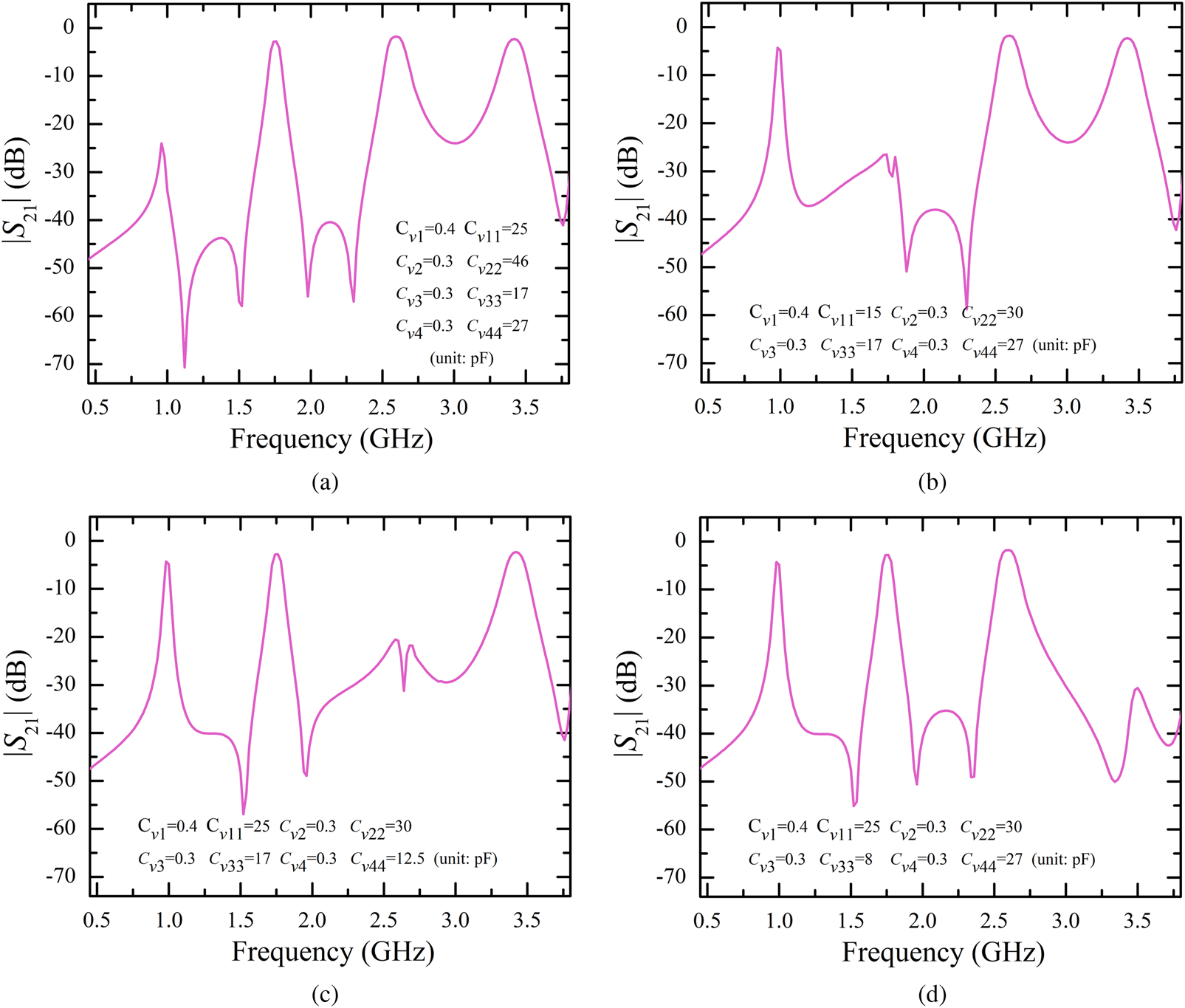
Figures 18(a)–18(d) present the full-wave EM simulated results of the presented TQ-BPF. The full-wave EM simulated results show that the RLs are better than 12 dB over the entire tuning range of all the passbands. The CF of the first passband is tuned from 0.94 to 1.06 GHz with the IL varying from 4.3 to 5 dB, the CF of the second passband is tuned from 1.66 to 1.98 GHz with the IL varying from 2.8 to 3.5 dB, the CF of the third passband is tuned from 2.26 to 2.82 GHz with the IL varying from 1.5 to 2.4 dB, and the CF of the fourth passband is tuned from 3.16 to 3.54 GHz with the IL varying from 2.1 to 3 dB. As can be seen in Figs 19(a)–19(d), the simulated responses of the first passband-OFF state, the second passband-OFF state, the third passband-OFF state, and the fourth passband-OFF state are sketched, respectively. In addition, it can be seen that several TZs appear between the four passbands, which can improve band–band isolation and harmonic rejection. The simulations of the TQ-BPF demonstrate that the proposed methodology is scalable to higher-selectivity developments.
Full-wave EM simulated results of the proposed TQ-BPF. (a) The tunable first passband with fixed second, third and fourth passbands (Cv 1 = 0.4 pF, Cv 11 = 25 pF, Cv 3 = 0.3 pF, Cv 33 = 17 pF, Cv 4 = 0.3 pF, and Cv 44 = 27 pF). (b) The tunable second passband with fixed first, third, and fourth passbands (Cv 2 = 0.3 pF, Cv 22 = 30 pF, Cv 3 = 0.3 pF, Cv 33 = 17 pF, Cv 4 = 0.3 pF, and Cv 44 = 27 pF). (c) The tunable third passband with fixed first, second, and fourth passbands (Cv 1 = 0.4 pF, Cv 11 = 25 pF, Cv 2 = 0.3 pF, Cv 22 = 30 pF, Cv 3 = 0.3 pF, and Cv 33 = 17 pF). (d) The tunable fourth passband with fixed first, second, and third passbands (Cv 1 = 0.4 pF, Cv 11 = 25 pF, Cv 2 = 0.3 pF, Cv 22 = 30 pF, Cv 4 = 0.3 pF, and Cv 44 = 27 pF).

Measured S-parameters responses of switchable characteristics. (a) The first passband turns off. (b) The second passband turns off. (c) The third passband turns off. (d) The fourth passband turns off.

Conclusion
A TD-BPF, a TT-BPF, and a TQ-BPF have been proposed. Tunability and switchability are achieved by changing the voltages of the varactors. In addition, all passbands can be controlled individually. The measurement results of the TD-BPF and TT-BPF agree well with full-wave EM simulated results. For TD-BPF, the measurement results indicate that the CF of the first passband is tuned from 1.37 to 1.62 GHz and the CF of the second passband is tuned from 2.3 to 2.64 GHz. In the designed TT-BPF, individual tuning ranges of CFs of three passbands are 1.3–1.5 GHz, 2.36–2.6 GHz, and 3–3.54 GHz. The proposed BPFs can be applicated to multiband applications with different operating frequencies. Furthermore, the proposed structure can be applied to the design of quint-band or more than quint-band tunable BPF in the future.
Acknowledgement
This work is supported in part by the National Natural Science Foundation of China with grant no. 61973173 and 61841108, Technology Research and Development Program of Tianjin with grant no. 18ZXZNGX00340, the 111 Project with grant no. B16027, the China-Europe Joint Research Centre for Solar PV Technology of Tianjin, the International Cooperation Base for New PV Technology, the Key Laboratory of Photoelectronic Thin Film Devices and Technology of Tianjin, and the Engineering Research Centre (Ministry of Education) of Thin Film Photo-electronics Technology.
 Zhao Li was born in Hohhot, Inner Mongolia province, China. She received the B.E. degree from Zhengzhou University, Zhengzhou, China, in 2018. She is currently working toward the M.E. degree at Nankai University, Tianjin, China. Her main research interest is tunable filters.
 LiTian Wang was born in Tianjin, China, in 1991. He is currently working toward the Ph.D. degree at Nankai University, Tianjin, China. His main research interests include multi-mode microwave filters, microstrip multiplexers, HTS bandpass filters, planar transversal bandpass filters, microwave substrate integrated waveguide filters, and tunable bandpass filters design.
 Ming He received the M.Eng. and Ph.D. degrees in electrical engineering from Nankai University, Tianjin, China, in 2002 and 2008, respectively. Since 1997, he has been with the Department of Electronics, Nankai University, Tianjin, China, where he became a Professor in 2016. From 2004 to 2009, he held several visiting research appointments in Juelich Research Center and Karlsruhe University, Germany. His research interests are in the fields of the applications of high-temperature superconductors, the generation and detection of THz signals, and microwave communications.
 XiaQing Li received her B.E. degree in Chang'an University of China, Xi'an, China, in 2018, and is currently working toward the M.E. degree in communication and information systems at Nankai University. Her main research interests are microwave differential filters.
 ZheLong Liang received his B.E. degree in communication engineering from Nankai University, Tianjin, China, in 2017, and is currently working toward the M.E. degree in communication and information systems at Nankai University. His main research interest is microwave balanced filters.
 ZhiPeng Wang was born in Anyang, Henan province, China, in 1996. He received the B.E. degree in electronic and information engineering from Northeast Agricultural University, Harbin, China, in 2017, and is currently working toward the M.E. degree at Nankai University, Tianjin, China. His major research interests include the design of microwave tunable filters and high temperature superconducting tunable filters.