The heat-assisted magnetic recording environment
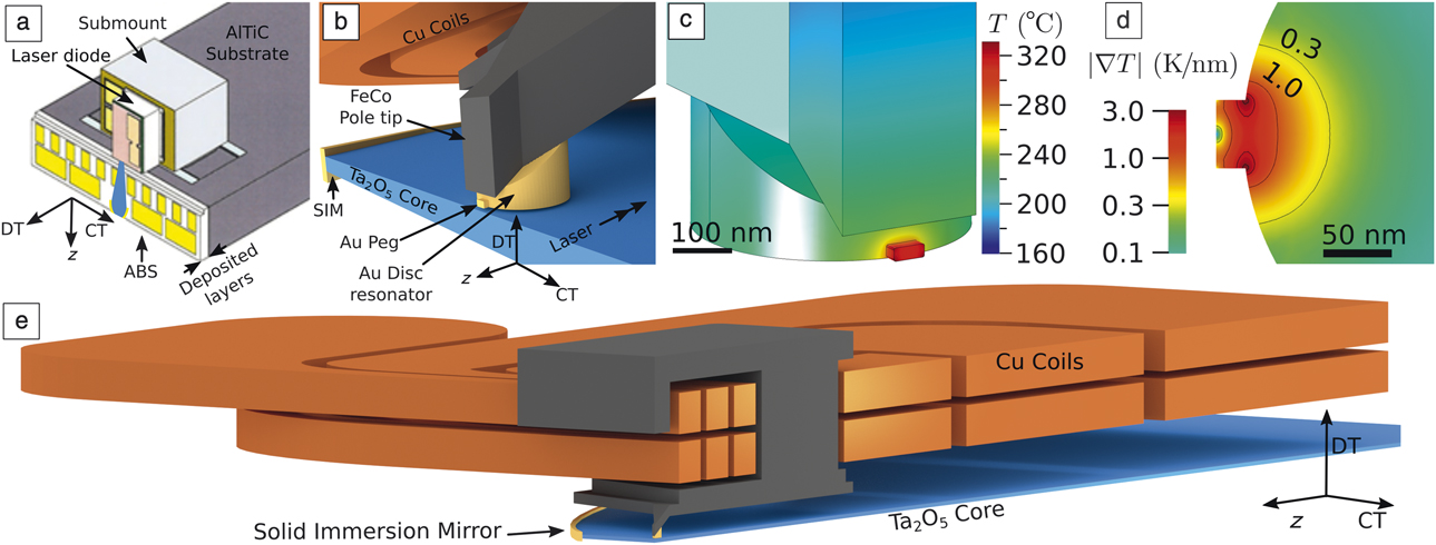
The geometry of a heat-assisted magnetic recording (HAMR) head is shown in Figure 1. The primary optical elements are the laser, focusing optics (“light path”), and near-field transducer (NFT). In a HAMR head, the magnetic localization and gradient problem of conventional perpendicular recording has been replaced with a thermal localization and gradient problem. The recording industry has favored plasmonic nanostructures as the primary technology to heat the recording layer. There are several categories of plasmonic NFTs; we focus here on the “lollipop” NFT, where the plasmon is generated on a circular disc and a rectangular peg is used for concentration.Reference Challener, Peng, Itagi, Karns, Peng, Peng, Yang, Zhu, Gokemeijer, Hsia, Ju, Rottmayer, Seigler and Gage1 The NFT peg heats the media, which is moving in the down-track (DT) direction, as shown in Figure 1a. The recording process happens in between the peg and the pole where the media is cooling and the magnetic field is strong.
Overview of a heat-assisted magnetic recording writer. (a) Recording head at 30× magnification. Approximate dimensions are 1.2-mm down-track (DT), 700-μm cross-track (CT), and 100-μm in z. Gold electrical connector pads are visible. The air-bearing surface (ABS) is on the underside (+z). Laser submount and laser diode are attached. Note the direction of the core (blue). Media moves in the +DT direction. (b) Zoomed version (30 kx) of the head showing the near-field transducer (NFT) (gold), magnetic pole tip (gray), copper coils (orange), and tantala (Ta2O5) core (blue). Note: SIM, solid immersion mirror. (c) Temperature of the NFT and pole given an input power of 15 mW (assuming 100% efficiency for the laser and light delivery system). (d) Cross section of the NFT showing the in-plane thermal gradients (i.e., orthogonal to the motion of the media). (e) Cross section through writer core, coils, NFT, and SIM.

At 10 K rpm (30 m/s), the NFT has ∼1 ns to provide enough power to the FePt recording layer in order to heat it past its Curie temperature of ∼400°C. The net power required to heat the track is approximately 0.15 mW. However, delivering the energy to the recording layer is only a few percent efficient,Reference Gosciniak, Mooney, Gubbins and Corbett2 resulting in tens of mW of optical power being absorbed by nanostructures in the head. In terms of the power flux density, the peg has ∼50-nm cross-track (CT) width and 25-nm DT height, leading to a power flux density of ∼150 TW/m2, some 25 million times higher than the surface of the sun. Figure 1c–d shows the impact of this power density on the NFT temperature, which has a peak value >300°C and thermal gradients that are locally >1 K/nm.
The impact of this extreme thermal environment on head engineering is profound. High temperatures adversely affect the reliability of the recording head through activation of many Arrhenius-type processes, including migrative (diffusion, interdiffusion, void migration), reactive (oxidation, reduction, corrosion), interfacial (interface reactions, migration of materials and voids along interfaces) and phase-change processes (amorphous to crystalline transitions). All of these can render irreversible head damage over time scales comparable to the aggregate hard-drive workload. The isothermal effects are further compounded by cyclic effects that are unavoidable since the laser must be temporarily reduced in power while the head is flying over the servo wedges that maintain the CT position to within 1–2 nm. Servo wedges are periodic magnetic patterns along the data tracks that are written into the media during drive manufacturing and serve to keep the head located and centered on a specified data track.
Further stress originates from the high-T-specific head–disc interaction. Mismatches in the coefficient of thermal expansion between materials in the vicinity of the NFT cause differential expansion as they equilibrate in temperature, causing highly nonuniform interfacial stresses and protrusion of the head at the air-bearing surface (ABS). However, not all differential protrusion is unwanted—the fly height is passively controlled by a pattern of channels that are etched into the underside of the slider (collectively, the pattern is referred to as the air bearing) and actively controlled by embedded heating elements, which are used to thermally expand portions of the slider, thereby protruding the reader or writer toward the media with <30 Å spacing.Reference Boettcher, Li, de Callafon and Talke3 The chemical environment of the head is also high pressure—the passive air bearing is generally maintained at >10 atmospheres, similar to the boiler in a steam locomotive, and rich in oxygen, water vapor, and lube fragments. Water and oxygen cannot simply be mitigated by the introduction of He-encased drives, as they are still present at the ppm level inside hermetically sealed He drives, which is more than enough to attack vulnerable materials.
In short, to meet drive industry-standard reliability specs, HAMR recording heads must maintain performance at hundreds of degrees Celsius in a high-pressure, reactive environment for many thousands of write power-on hours (hours where the laser and magnetic write coils are active, does not include reading or idle time). In the next sections, we describe the challenges associated with materials selection for operation in these harsh environments.
Light path
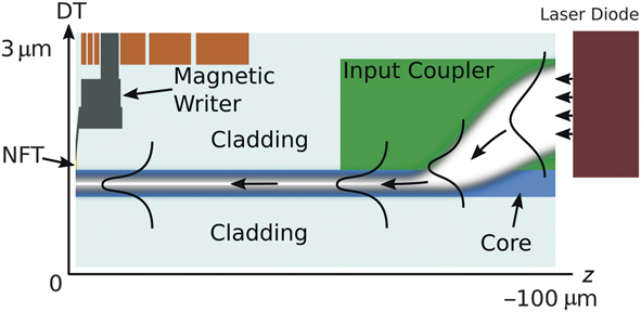
The HAMR recording process begins with the delivery of near-infrared (IR) light (∼800 nm) from the laser’s emitter facet at the back of the head through the slider to the NFT at the ABS. This constitutes a path length of ∼100 µm with transit through several optical elements, as shown in Figure 2. To accommodate positional variances of the laser submount on the slider during assembly, the laser spot is first collected using a thick input coupler. This layer is a mid-refractive-index material (n ∼ 1.6–1.9) that is large enough dimensionally to capture the ∼1–2-µm laser spot mode profile. This layer vertically guides the light, forcing it into a tightly confined mode inside a planar waveguide of high-index core and low-index clad layers. The light propagates down this waveguide until it reaches a parabolic solid immersion mirror, at which point it is focused in the CT direction so that the evanescent tail of light that leaks from the core illuminates the NFT.Reference Challener, Peng, Itagi, Karns, Peng, Peng, Yang, Zhu, Gokemeijer, Hsia, Ju, Rottmayer, Seigler and Gage1
Light delivery system. Cross section of the recording head showing the coupling of light from the laser to the guided core mode via the input coupler. Aspect ratio is compressed for clarity. Note: NFT, near-field transducer; DT, down-track.

To minimize laser power and avoid undue heating, high-quality dielectrics with low propagation loss are required. This corresponds to deposited films with extinction coefficient k < 10–4 (where k is the imaginary part of the refractive index). This is most often achieved using hot reactive physical vapor deposition (PVD) or chemical vapor deposition/atomic layer deposition (CVD/ALD) processes for high film density and low impurities. Deposition T(T dep) is kept <300°C to avoid damage to the read sensor. Absolute k alone, however, is not sufficient due to structural confinement of the light—proper geometry selection, low patterned line edge roughness from etching, and maintenance of clean interface layers are all critical elements to ensure high efficiency. With these practices, propagation losses below 20 dB/cm can now be routinely achieved in devices.
Materials selection for the coupler and waveguide elements is governed by a wide set of requirements that span process requirements (T dep, uniformity, step coverage, deposition rate), film properties (index, loss, stress, adhesion, interface composition), and device performance (ABS recession, chemical and thermal stability). Input couplers are often selected from the SiOxNy system due to its flexibility in composition and refractive index (n = 1.45–2.0, achieved by blending the terminal SiO2 and Si3N4 compounds). SiOxNy also benefits from the availability of established high-rate CVD or PVD techniques and manufacturable patterning schemes.
For core layers, a wider set of materials options exists. In general, n > 2 for the core layer is desirable for confinement, which implies a bandgap >1.6 eV for laser wavelengths in the near IR. Among known high-index materials,Reference Baranov, Zuev, Lepeshov, Kotov, Krasnok, Evlyukhin and Chichkov4 this excludes Ge, antimonides, and tellurides outright. Amorphous silicon is also impractical on the basis of k values in the 0.01–0.5 range around 800 nm.Reference Bruynooghe, Schmidt, Sundermann, Becker and Spinzig5 This leaves oxides, nitrides, selenides, and halides as potential candidates. The HAMR community has focused on metal oxides, specifically d-band oxides such as Ta2O5. In these materials, d-band electrons contribute to electronic polarizability, which increases n. The lower unpaired p-electron count compared to group IV and group V compounds also promotes higher bandgap and sharper band edges, both of which lead to low k. When these materials are deposited using existing CVD, PVD, and ALD equipment, they form amorphous layers with low optical loss and crystallization temperatures that typically exceed 500°C, reducing the risk for irreversible increase of the propagation loss during the service life of the head. They also present the best resistance to chemical attack from wafer-level patterning and to ABS reaction during operation. At present, PVD Ta2O5 with n ∼ 2.1 is a common core option that is relatively robust so that core material failure at the ABS is not a limiter for head lifetimes.
Cladding layers, in contrast, have relatively fewer candidates, but have more critical requirements. In addition to low index and loss, they must be controllable in thickness and uniformity down to the nanometer level, must provide good adhesion to and chemical stability with the NFT metallization, must be more environmentally durable due to direct proximity to the hot NFT, and in some cases, must be capable of optical-quality growth over NFT topography. Materials satisfying these requirements are scarce. Dense, low-index materials generally comprise fluorides (n = 1.37–1.5), MgO (n = 1.7), SiO2 (n = 1.45), and Al2O3 (n = 1.65). The fluorides and MgO are extremely susceptible to hydrothermal corrosion and cannot survive either wafer integration or ABS operation. As a result, HAMR designs have focused on SiO2 and Al2O3.
Common deposition techniques, including PVD, reactive-PVD, ALD, and plasma-enhanced atomic layer deposition, are all capable of producing amorphous, low-loss films with crystallization thresholds above 500°C. The preferred use of either material depends on the efficiency of the NFT design as well as the maximum operating temperature of the head. Despite these materials finding common use in structural or extreme environmental applications due to their thermodynamic stability, they can be converted to low-density or volatile hydroxides in the HAMR recording environment. Clad-layer pitting near the NFT, and clad-NFT metal high-T adhesion failures are common failure modes. It is expected, however, with proper NFT design and heat sinking, that these oxides will satisfy initial-generation HAMR head requirements. Exploration of alternative robust low-loss materials (e.g., mixed-metal oxides) remains an appealing area of work.
NFT materials
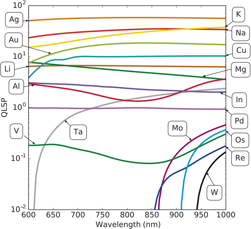
The NFT functions by coupling the energy of incident photons in the lightpath into surface plasmons. The efficiency of this process depends on the geometry of the transducer and the focusing capability of the solid immersion mirror. To a good approximation, the resonance strength of a nanostructure such as the lollipop can be approximated by the peak polarizability of a small, isotropic nanoparticle—this is often referred to as the quality factor of a localized surface plasmon (QLSP) = –Re(ε)/Im(ε).Reference Arnold and Blaber6 For good metals (i.e., those without strong interband absorption at the wavelength of interest), the real part of the complex permittivity describes the carrier density (Re(ε) = n 2–k 2) and the imaginary part describes the electron scattering losses (Im(ε) = 2 nk). Metals with high concentration of free electrons are generally preferred to increase the magnitude of Re(ε) for a stronger resonance, but this must be balanced with increased self-heating caused by electron scattering from the high density of states at the Fermi level. An optically ideal plasmonic material with large negative Re(ε) and minimum Im(ε) corresponds to one with minimum n and maximum k. It should be noted that the use of tabulated optical and thermal properties for NFT materials selection can be dangerous as both depend on size,Reference Link and El-Sayed7,Reference Westcott, Jackson, Radloff and Halas8 temperature,Reference Eragamreddy, Guler, Chaudhuri, Dutta, Kildishev, Shalaev and Boltasseva9 and film quality.Reference Sönnichsen, Franzl, Wilk, von Plessen, Feldmann, Wilson and Mulvaney10,Reference Foerster, Joplin, Kaefer, Celiksoy, Link and Sönnichsen11 Where possible, empirical determination of these constants under device-like thicknesses and temperature is recommended (e.g., via spectroscopic ellipsometry).
NFT materials selection is complicated by several other factors. First, the economic restriction of an adequate high-volume supply of commercial diode lasers mandates that QLSP be high toward the red end of the electromagnetic spectrum (>700 nm). Second, the NFT materials must be robust against the reactive ABS environment, implying a necessary minimum level of noble character. Finally, the peg, disc, and heatsink are complex three-dimensional structures with dimensions in the tens to hundreds of nanometers, so grain and morphological stability of the NFT are of primary importance. Note that single-crystal materials are impractical due to the sub-300°C thermal limit associated with irreversible instability in the read sensor in modern heads. As a result, textured polycrystalline films are the norm; 10–100-nm median grain sizes result, with many high-angle grain boundaries and nonequilibrium defects. Optically, this microstructure can cause a ∼2× reduction in plasmon propagation length.Reference Kuttge, Lezec, Atwater and Polman12 It also follows that in such polycrystalline, high surface area:volume nanostructures, the activation energies associated with grain boundaries, surfaces, and bulk diffusion should be as high as possible to combat texture reorientation, grain growth, and reshaping.
Figure 3 shows QLSP for a variety of common conductors.Reference Palik13–Reference Weaver and Frederikse15 Gold is the most common choice for the NFT material due to its combination of moderately high free-electron density, very low electron–phonon coupling, high-energy interband transitions, excellent thermal conductivity, and strong resistance to oxidation. It is also readily deposited and etched using conventional nanofabrication techniques. Many of the pioneering demonstrations of HAMR to date have been performed with Au NFTs.Reference Challener, Peng, Itagi, Karns, Peng, Peng, Yang, Zhu, Gokemeijer, Hsia, Ju, Rottmayer, Seigler and Gage1,Reference Wu, Kubota, Klemmer, Rausch, Peng, Peng, Karns, Zhu, Ding, Chang, Zhao, Zhou, Gao, Thiele, Seigler, Ju and Gage16
Quality factor of a localized surface plasmon (QLSP) of a variety of conductors that have QLSP >3 at some wavelength (based on tabulated optical constants from Palik,Reference Palik13 Johnson and Christy,Reference Johnson and Christy14 and Weaver and FrederikseReference Weaver and Frederikse15). QLSP >∼10 is required for optimal near-field transducer performance.

Implementation of Au poses serious challenges. The intrinsic absorption losses in Au that drive self-heating are amplified by increased diffuse electron scattering from nanoscale grain boundaries and edge defects caused during fabrication. It is also difficult to deposit Au with near-bulk density due to fine-grained Volmer–Weber (island) growth modes on horizontal amorphous dielectric surfaces and Thornton model zone-1 growth (columnar growth with intergranular voiding) on vertical side walls of trench or liftoff structures.Reference Kossoy, Simakov, Olafsson and Leosson17–Reference Karabacak, Wang and Lu19 Further, gold has very poor adhesion to most materials due to the absence of electronic bonding states, and has very low diffusion activation energies (E surface ∼ 0.5 eV, E internal ∼ 1 eV, E grain boundary ∼ 0.9 eV, E lattice ∼ 1.8 eV).Reference Gupta20–Reference Huang, Lilley, Divan and Bode22 As a result of these factors, Au nanostructures are often morphologically unstable at high temperature, as evidenced by myriad reports of spontaneous reshaping,Reference Taylor, Siddiquee and Chon23 blunting,Reference Im and Oh24 or breakup.Reference Nichols and Mullins25–Reference Karim, Toimil-Molares, Ensinger, Balogh, Cornelius, Khan and Neumann27
In the context of HAMR, low diffusion activation energy coupled with underdensity in the body of the NFT produce atom and vacancy flows that are sufficient to enable voids to nucleate at the hot end of the peg. This ultimately results in the detachment of the peg from the ABS followed by complete recession of the peg into the head (Figure 4). A sizable portion of research in the HAMR industry during the last five years has been focused on devising countermeasures to this problem.
Transmission electron microscope image of an Au near-field transducer (NFT) peg partially recessed from the air-bearing surface. Recession increases NFT-media spacing, leading to degraded recording performance, increased laser power/temperature rise, and eventual head failure. Image is 200-nm wide.

Possible solutions to peg recession involve the application of traditional metallurgical concepts on the nanoscale to improve high-temperature robustness. Care must be taken not to impact the thermal or optical properties of the material in ways that offset the increased microstructural stability with increased temperature, resulting in a net power-on-hour loss. Au-X alloys that facilitate solid-solution strengthening, precipitation hardening, and grain-boundary segregation to improve grain stability have all been broadly explored. Fully miscible systems of strong plasmonic metals such as AuCu and AuAg often result in a net stability loss across a majority of the concentration range due to increased electron-defect scattering in the alloy. Alloys with dopants for grain-boundary pinning such as AuTi, AuNi, or AuCoReference Hirata, Hosoi, Kawamori and Roppongi28 invariably suffer deterioration in the optical and thermal properties, limiting their useful concentration range to ∼<5 at.%, but judicious selection has been demonstrated to improve head lifetimes up to ∼10×. In addition to alloying, film-growth process optimization and the use of subnanometer seed layers for texture control and density improvement can provide additional gains.
The use of interface adhesives to overcome poor Au-dielectric adhesion and retard interface diffusion has also been reported.Reference Ji, Xu, Cen, Ying and Toh29 Typically, these are sub-1-nm thickness transition metals such as Cr, Ti, or Ta applied carefully in the fabrication process to avoid oxidation. Here, a balance must be struck between improved adhesion and the maintenance of low loss at interfaces where the fields are strongest.Reference Aouani, Wenger, Gerard, Rigneault, Devaux, Ebbesen, Mahdavi, Xu and Blair30,Reference Habteyes, Dhuey, Wood, Gargas, Cabrini, Schuck, Alivisatos and Leone31 Adhesion materials can improve interfacial thermal conductance between Au and dielectric by 2–4× by improving phonon transmission,Reference Jeong, Freedman, Liang, Chow, Sokalski, Bain and Malen32 but increased thermal heating from plasmon damping in these lossy materials (2–7× higher), gradual poisoning of the NFT metal by the adhesive, and loss of adhesion due to oxidation from the ABS can limit the long-term upside and must be managed.
Alternatives to Au for high-Q plasmonic applications have been widely researched.Reference Blaber, Arnold and Ford33–Reference Naik, Shalaev and Boltasseva35 Of the conductive metals, Cu, Ag, and Al can compete with or even outperform Au on an optical basis over some wavelength ranges. Cu and Ag compete in the near IR, but readily form nonpassivating oxides and are prone to sulfidation, hampering their use at the ABS. Alloys of these metals have yet to achieve sufficient corrosion resistance while still outperforming Au. Al, despite forming a robust ∼2-nm passivating surface oxide, exhibits a high-loss interband transition, which extends across much of the near IR. Refractory nitrides have also garnered much recent attention as attractive high-temperature plasmonic materials.Reference Naik, Kim and Boltasseva36,Reference Guler, Boltasseva and Shalaev37 TiN and ZrN have QLSP values ∼5–10× worse than for Au13 and also have reduced thermal conductivities, which result in laser-induced temperature rises that are ∼6–8× higher than all-Au structures. Under these conditions, the integrity of other structures adjacent to the NFT, notably the write pole, clad layers, and head overcoat, can be compromised. The loss of the overcoat is particularly harmful as metal nitrides tend to convert to nonpassivating oxynitrides under prolonged heat exposure. Last, heavily doped conducting oxides have also been considered for plasmonic applications, but generally cannot achieve high enough carrier concentrations while remaining single phase at high temperatures.Reference Naik, Kim and Boltasseva36
Despite these challenges, the hard-drive industry has demonstrated >1000 write power-on hour drivesReference Rausch, Chu, Lu, Puranam, Nagulapally, Lammers, Dykes and Gage38 and is approaching industry-standard reliability requirements. It is currently unlikely that any of the previously discussed alternative materials will surpass Au as the dominant NFT material in early-generation HAMR heads. However, in order to ensure the extendability of HAMR to higher areal densities (and hence smaller pegs), more research is needed to develop high-QLSP, low-loss, thermally stable materials.
Summary
The aim of this article was to provide an overview of some of the materials challenges associated with HAMR recording heads. HAMR has required substantial innovation in materials and processing technologies due to the addition of the light-delivery infrastructure, high-temperature NFT, and extreme recording environment. Tremendous progress has been made, with the industry adapting well to the introduction of new optical and plasmonic materials and processes. NFT materials remain the greatest single challenge, but are approaching product-level specifications. We continue to look to the wider materials community for innovations in robust, low-loss plasmonic materials, metal–oxide interface adhesives, durable optical-grade oxides, and low-T deposition technologies for improved film density.

Michael Kautzky is the managing technologist of the Thin Film Development Group at Seagate Technology. He received his PhD degree in materials science and engineering from Stanford University. His research focuses on advanced thin-film materials and deposition development, wafer-level recording head integration, and novel thin-film characterization. He is a holder of 94 issued US patents. Kautzky can be reached by email at michael.c.kautzky@seagate.com.

Martin Blaber is a staff engineer in the Transducer Development Group at Seagate Technology. He received his PhD degree in physics from the University of Technology Sydney, Australia. He has published more than 30 articles on the electronic structure of plasmonic materials and the optical response of interacting plasmonic systems. Blaber can be reached by email at martin.blaber@seagate.com.