Introduction
The performance of modern wireless communication systems needs to be improved enormously due to the increase in applications demanding high-speed, multi-function, wide bandwidth and frequency tuning. In 5G and subsequent wireless networks, traditional antenna designs and their single-band radiation are inadequate. A compact, dual band with circularly polarized (CP) antenna suits well to meet the 5G and beyond 5G applications such as Internet of Things (IOT) devices, vehicular communications, satellite communication, military and defense applications [Reference Gao, Clark, Unwin, Zackrisson, Shiroma, Akagi, Maynard, Garner, Boccia, Amendola, Massa, Underwood, Brenchley, Pointer and Sweeting1]. Design and development of an antenna with dual band can be a challenging task, due to their conflicting requirements of multi-band radiation, impedance matching, and radiation pattern consistency over the radiating bands [Reference Balanis2].
An antenna array or MIMO antennas are used to achieve dual resonant, wide bandwidth and gain enhancement. However, these techniques are prone to mutual coupling and Electromagnetic Interference (EMI) [Reference Zhou, Zhao, Ning and Bao3]. In order to enhance the connectivity in a Wi-Fi and radio frequency identification (RFID), a dual band antenna with compact size is needed. Also, other portable devices such as wireless routers require dual band antenna with circular polarization [Reference Yang, Qi, Chen and Li4].
For the past few years, the application of RFID antennas for Wi-Fi and iPads are gaining popularity particularly in ultra-high-frequency (UHF) and high-frequency spectrums [Reference Bhaskar and Singh5]. Therefore, the investigation of RFID antennas and its enhanced radiation characteristics are of prime importance. The RFID plays a key role in many applications such as defense, industries, and health care. The antenna is a vital part of an RFID system that helps the RFID reader to communicate with its tags in a dependable and effective manner [Reference Barman, Bhaskar and Singh6]. Due to its compactness, low profile, low power handling capacity and ease of integration, microstrip antennas are preferred often in RFID systems [Reference Nguyen, Lin, Chen, Chang and Chen7].
CP antennas offer greater flexibility for RFID reader and tag applications than linearly polarized antennas due to their insensitivity to angular orientation. Traditionally, CP waves are generated by turning on few orthogonal linearly polarized modes at the same time, each with same amplitude and a phase difference of 90° is done using slots [Reference Bajaj, Upadhyay, Kumar and Kanaujia8], power divider-based feed network [Reference Lerkbangplad, Namahoot, Akkaraekthalin and Chalermwisutkul9]. However, achieving CP using phase shifters and power dividers increases the design complexity and needs large size.
In [Reference Wang, She, Han, Fang and Liu10] and [Reference Pan and Dong11], dual-band antenna is designed using stacked patch antenna in which the two patches are made at right angles to one another to achieve CP, whereas stacked structure introduces high profile leading to impedance matching complexity over a wide range of frequency. The CP can also be achieved by truncating the patch and Defecting Ground Surface [Reference Le, Ahmed, Ukkonen and Björninen12]. However, the radiation efficiency and pattern get reduced proportionally. In [Reference Sarkar and Gupta13],CP and dual-band operation are achieved by positioning perpendicular slots in the circular patch and the ground. These slots help to achieve CP, whereas the gain gets affected due to the back and side lobes. In order to enhance this gain, an Artificial Magnetic Conductor (AMC) is introduced below the antenna which increases the overall size of the configuration.
CP RFID reader with wide beam width response is preferred for IOT applications. For that, the radiating patch with ring delay lines and parasitic patches are used, which reduces the reliability and compactness of the design [Reference Lai, Yang and Chen14–Reference Birwal, Singh, Kanaujia and Kumar17]. Further, electromagnetic band gap (EBG) structures are used to achieve CP [Reference Zheng, Guo, Vandenbosch and Ding18] and [Reference Yi and Qu19], however introducing EBG structures also increases the size of the configuration. In [Reference SalarRahimi, Rashed-Mohassel and Edalatipour20], circularly symmetric EBG structures are introduced around the patch to achieve CP, whereas this induces coupling effects due to inefficient surface wave suppression. In [Reference Ellis21], asymmetric ground plane is used to produce CP and which increases the cross polarization in radiation pattern which degrades the CP quality. Similarly, CP is achieved using asymmetric ground plane and the compact slits helps to maintain the size and cross polarization levels in [Reference Koohestani, Azadi-Tinat and Skrivervik22]. However, this arrangement has a limited gain due to the ohmic loses.
In the proposed work, the synergistic effects of both asymmetric ground plane and EBG structures are utilized to achieve the CP without increasing the size and complexity. Asymmetric ground plane introduces phase difference for circular polarization, while EBG structures enhance the quality of the CP by reducing the surface wave and cross-polarization. The asymmetric ground plane disrupts the uniform propagation of surface current, and the EBG structure suppresses them, leading to isolation and reduced EMI.
Moreover, the read range of the antenna for RFID applications are not discussed in the recently reported literature. The read range of the antenna is an important parameter for RFID. Therefore, the read range analysis and experimental validation is carried out in our proposed work. The read range purely depends on the gain of the antenna, type of the RFID, power, and the environment. Hence, to increase the read range of the antenna, the gain of the antenna has to be improved. In [Reference Alibakhshikenari23] and [Reference Ding, Zhang and Ma24] the parasitic patches and AMC based Conductor backed CPW techniques are employed respectively to enhance the gain of the antenna. Besides, these techniques are effective for the read range enhancement only for the narrow band linearly polarized RFID applications.
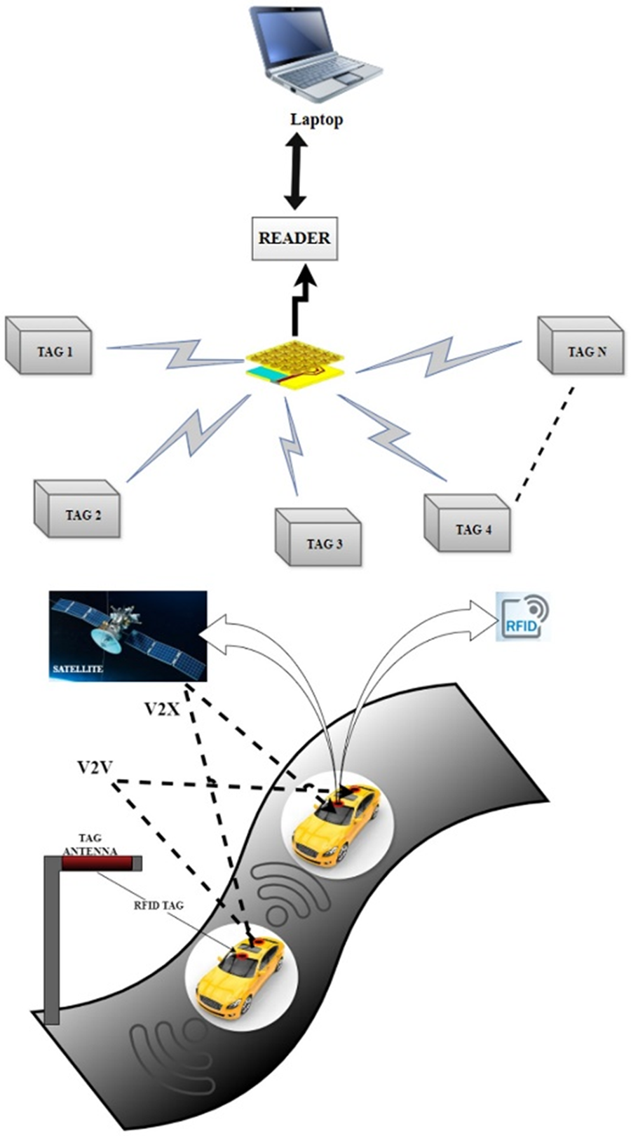
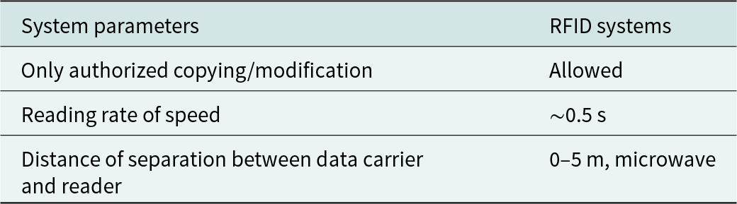
In the proposed work, a dual layer metasurface (MS)-based radiating patch is proposed to enhance the gain and bandwidth of the antenna in both lower and upper spectrum for RFID applications. The top and bottom layer of the MS is complementary to each other which produce a constructive interference in the desired direction thus improving the gain of the antenna. This kind of high gain antenna is a good solution for RFID reader applications such as vehicle identification and parking and Toll payment systems. Few merits of the proposed antenna used in RFID systems over the other recently reported works are listed in the Table 1. The architecture of CP with wide bandwidth antenna loaded RFID based IOT applications is shown in Fig. 1.
Antenna with RFID system architecture.

RFID system advantages over other systems

In this article, a novel CPW fed CP hexagonal shaped patch antenna with MS is proposed to radiate dual band for RFID applications. This prototype radiates in two different frequency bands ranging 2.09–2.88 GHz and 8–12 GHz with the bandwidth of 796 MHz and 4.24 GHz respectively. The lower frequency band centered at 2.45 GHz is used for RFID applications such as vehicle identification and parking and Toll payment systems, and the upper frequency band centered at 11.4 GHz, is used for X-band applications such as weather radar, police radar, and maritime radar. By employing asymmetric ground plane and EBG structure, a proper circular polarization is achieved in both the lower and upper frequency spectrum. A novel MS is designed and used in the antenna design to enhance gain and bandwidth in both lower and upper frequency spectrum. The proposed antenna is simulated, fabricated and experimentally validated. Also, the proposed antenna read range and its radiating characteristics are tested in a real time environment and in the testing different types of tagged items used with in a read range. The performance is compared with an extensive survey of state-of-the-art RFID based works.
Antenna design
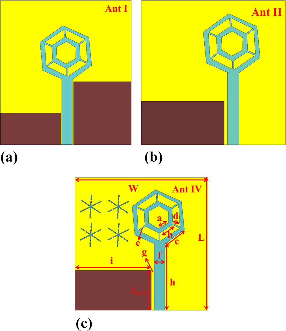
The proposed antenna in its evolution stage from the basic CPW fed monopole structure is illustrated in Fig. 2. Rogers RT/Duroid 5880 ( ${\varepsilon _r} = 2.2)$ of thickness 1.6 mm is used as a substrate to etch the radiating patch with CPW fed as depicted in Fig. 2(a) (Ant. I).
Proposed antenna top view in evolution stages (a) Ant I, (b) Ant II, (c) Ant III.

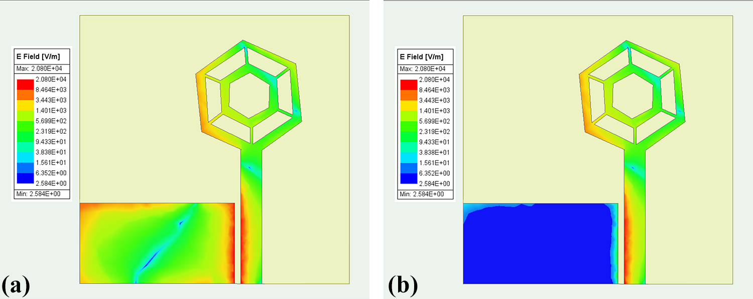
To improve impedance matching and wide bandwidth, asymmetric ground plane is employed as depicted in Fig. 2(b) (Ant. II). The new resonance at 2.45 GHz arises due to the modified current path and field distribution caused by the ground plane asymmetry. The asymmetry creates additional localized modes, which combine with the primary resonance. Figure 3 show plots of the current distribution at the new resonance frequency (2.45 GHz) and its comparison with the distributions at the primary resonance.
Surface current distribution during evolution stages (a) Ant II at 2.45 GHz, (b) Ant II at 9.5 GHz.

Parametric analysis to achieve CP
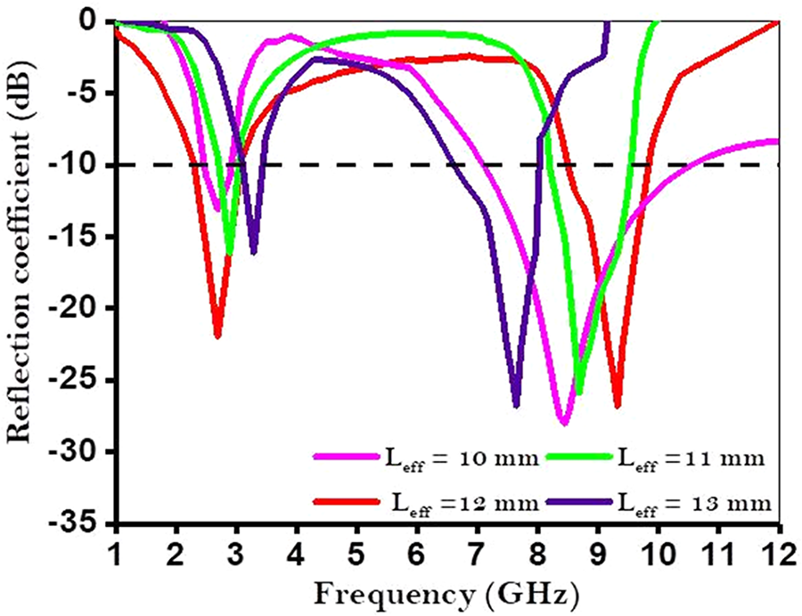
Equation (1) directly correlates the resonance frequency with the effective electrical length (L eff) which is influenced by the ground plane dimensions. In planar antenna designs, the physical ground plane size contributes to L eff through fringing fields and edge effects. A reduced ground plane length results in a higher resonance frequency, while an extended ground plane lowers it. Our simulation results, shown in Fig. 4, confirm this behavior, where modifying the ground plane length caused a proportional shift in the resonance frequency, consistent with Equation (1). This correlation highlights the importance of ground plane size in tuning the antenna’s operating frequency:
 \begin{equation}{f_r} = \frac{c}{{2{L_{eff}}\sqrt {{\varepsilon _{eff}}} }}.\end{equation}
Effect of ground width (L eff) variation on reflection coefficient characteristics.

The resonance introduced by the asymmetric ground plane can be analyzed using Equation (1), which defines the resonance frequency (f r) in terms of the effective resonant length (L eff) and effective permittivity (ε eff).
The introduction of an asymmetric ground plane modifies the boundary conditions, altering the surface current distribution on the antenna. This change effectively increases the resonant length (L eff) by extending the current path, which in turn reduces the resonance frequency as predicted by Equation (1). Additionally, the asymmetric geometry perturbs the effective permittivity by introducing field distortions and coupling effects, contributing to the emergence of a new resonant mode. The observed frequency shift to 2.45 GHz corresponds to this increase in L eff, confirming the theoretical prediction. The variations in resonance frequency with respect to changes in L eff are illustrated in Fig. 4, demonstrating a clear correlation with Equation (1).
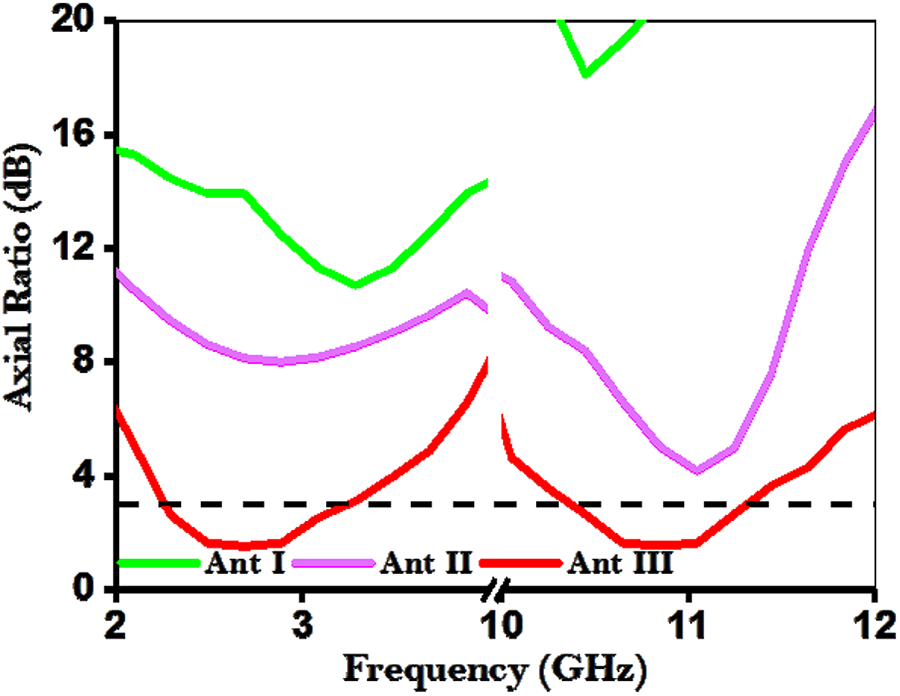
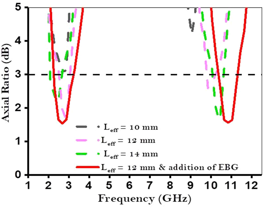
To achieve circular polarization in the operating bandwidth, the EBG structures are incorporated in Ant. II as depicted in Fig. 2(c) (Ant. III). An electromagnetic coupling is introduced between the asymmetric ground plane and EBG structure which provides circular polarization. In literature [Reference Zheng, Guo, Vandenbosch and Ding18–Reference SalarRahimi, Rashed-Mohassel and Edalatipour20], EBG structures are employed to achieve CP and all these works CP is achieved only in single band response. Whereas in our proposed work, asymmetric ground plane and EBG structure are used to achieve dual-band CP. The axial ratio response with and without EBG structure is plotted in the Fig. 5. The effect of the asymmetric ground height and addition of EBG structures are plotted in the Fig. 6.
Axial ratio characteristics of evolution stages.

Axial ratio variation due to asymmetric ground plane and EBG structure.

Design of dual layer MS
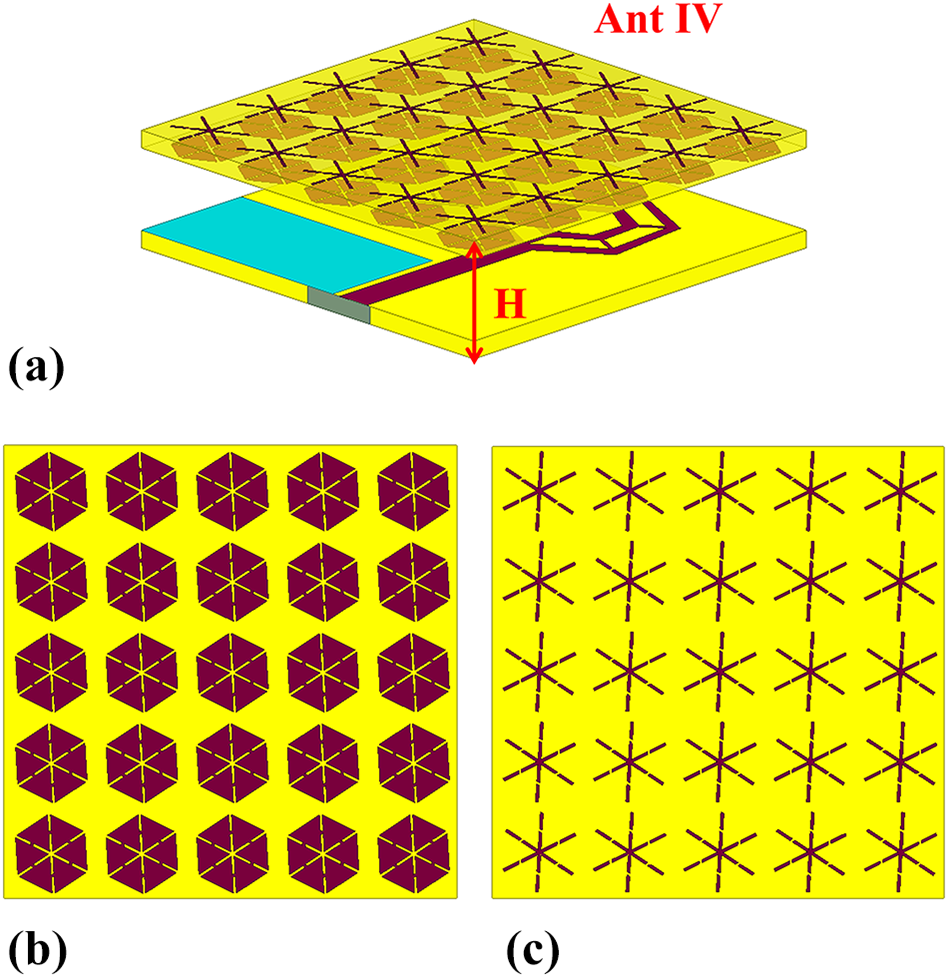
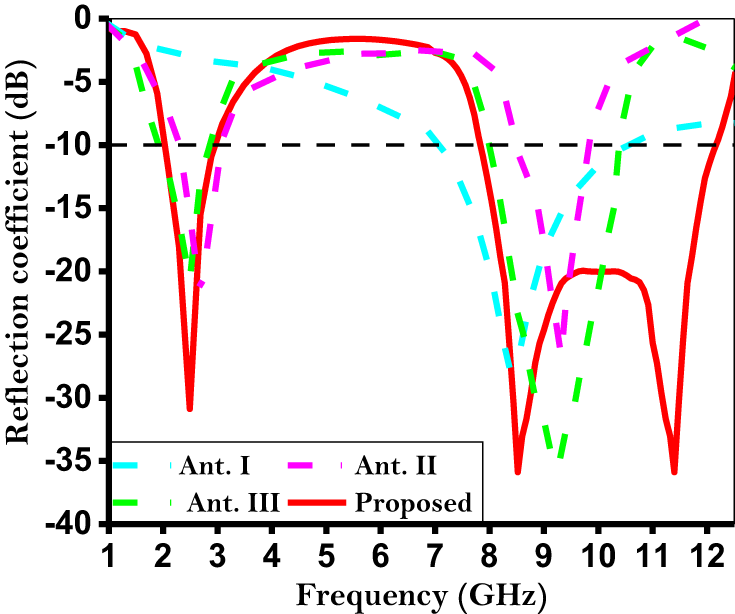
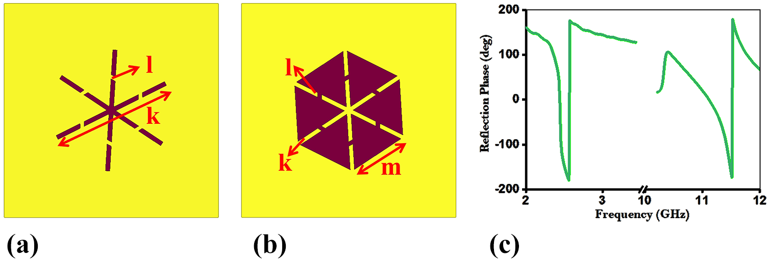
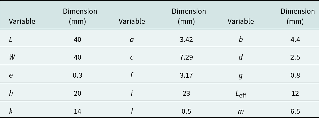
Antenna III is loaded with MS to enhance the average gain value as illustrated in Fig. 7(a) (Ant. IV). The reflection coefficient of the antenna’s evolution stages are plotted in the Fig. 8 .This design consists MS fabricated on Rogers RT/Duroid 5880 in which the top and bottom side is etched with complementary hexagonal structures. The top is an array of 6 × 6 hexagonal-shaped unit cells Fig. 7(b), whereas the bottom is an array of 6 × 6 asterisk-shaped unit cells Fig. 7(c) are designed and fabricated. These structures are complementary to each other whose unit cell structure and its material characteristics are shown is Figs. 9(a), (b) and 10 respectively. The unit cell dimensions are optimized to realize positive phase gradient using Finite Element method based numerically simulated software (ANSYS HFSS.V.2024 R1) and these optimized physical dimensions are listed in Table 2 whose electrical dimension is 0.48 λ g × 0.48 λ g × 0.02 λ g.
Proposed antenna: (a) perspective view with metasurface; (b) metasurface top view; (c) metasurface bottom view.

Reflection coefficient characteristics of evolution stages.

Unit cell structure: (a) top view, (b) bottom view, (c) reflection phase.

Optimized dimensions of the variables

The physical shape, dimension and location of MS are designed such a way to enhance the gain and bandwidth of the antenna. The MS is a periodic geometrical structure, which controls the electromagnetic waves such as phase, amplitude, and polarization etc. [Reference Abdullah, Xiao and Amaya25]. Using these properties in antenna design the antenna aperture, radiation pattern, gain and bandwidth are enhanced as referred in [Reference Samantaray, Ghosh and Bhattacharyya26] and [Reference Samantaray and Bhattacharyya27]. By using these properties, we proposed double layered MS for gain and bandwidth enhancement. Also MS employed antenna design exhibits the radiation in specific directions, which improves the antenna’s directivity and gain without needing to physically increase the size of the antenna. In our proposed work antenna gain is improved by providing a specific phase gradient and constructive interference in the desired direction.
These reflection phase plots and it’s in phase response with antenna wave are illustrated in the Fig. 9(c). The hexagonal unit cell (printed on the bottom side of the substrate) is designed and optimized to exhibits 0° reflection phase at 2.45 GHz (center frequency). Similarly, the asterix shaped unit cell (printed on the bottom side of the substrate) is designed and exhibits 0° reflection phase at 11.4 GHz (center frequency). Thus, it produces in phase gradient and constructive interference in lower band (2–3 GHz) and upper band (10–12 GHz) which reduces the reflection loss and enhances the directive gain of the antenna.
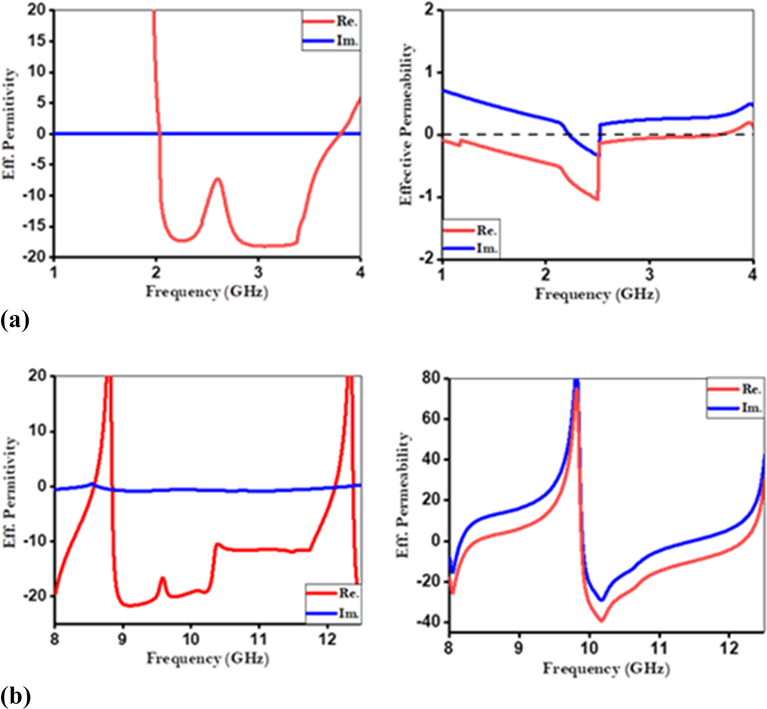
The gain and bandwidth of the proposed work is enhanced by using MS. In order to know significance and working of the MS we need to analyses the unit cell characteristics. Figure 10 illustrates the unit cell negative permittivity and permeability characteristics. The proposed MS has negative permittivity ranging 2–4 GHz and 8.5–12 GHz. Similarly, negative permeability is observed ranging 1–3.5 GHz and 10–12 GHz. From these, negative permittivity and permeability exhibits in-phase to the antenna surface current distribution. So that the total directive gain and bandwidth of the system is enhanced in a particular direction.
Unit cell effective permittivity and permeability characteristics: (a) hexagonal shaped unit cell; (b) asterisk shaped unit cell.

Therefore, the unit cell analysis is used to identify the structure exhibits negative refractive index characteristics in the radiating spectrum. These allows them to focus electromagnetic waves, reduce diffraction losses, scattering losses and surface wave propagation, ensuring that more radiated energy is directed in to the desired direction. Thus the MS leads to enhance bandwidth and gain.
By ray theory, the resonance frequency of the MS based antenna can be expressed using (2) [Reference Wang, Liu, Wu, Talbi, Zeng and Xu28]. The distance H between the antenna substrate and MS substrate is determined using the Equation (2). This expression has a relationship between frequency and distance. From [Reference Wang, Liu, Wu, Talbi, Zeng and Xu28], the operating frequency depends on the following equation,
 \begin{equation}f = {\text{ }}\frac{c}{{4\pi H}}\left( {{\emptyset _{MS}} + {\emptyset _{GND}} - 2N\pi } \right),{\text{ }}N = 0,1,2\end{equation}
where ϕMS and ϕGND are phase variation in the MS and ground plane and H is the distance between the MS and the antenna.
Figure 11 demonstrates the parametric analysis of the antenna by varying the MS location. It is observed that, at distance 9 mm, the (S11) has better impedance matching in both lower and upper band spectrums. The response of the antenna without MS is also included in the same graph to observe the significance of the MS. Varying the height H from 5 mm to 13 mm, the reflection coefficient and gain response get enhanced as depicted in the Figs. 11 and 12. From this parametric analysis at 9 mm, the MS exhibits in-phase to the antenna and current distribution which provides wide bandwidth and enhanced gain.
Metasurface reflection coefficient parametric analysis.

Metasurface gain parametric analysis.

Results and discussion
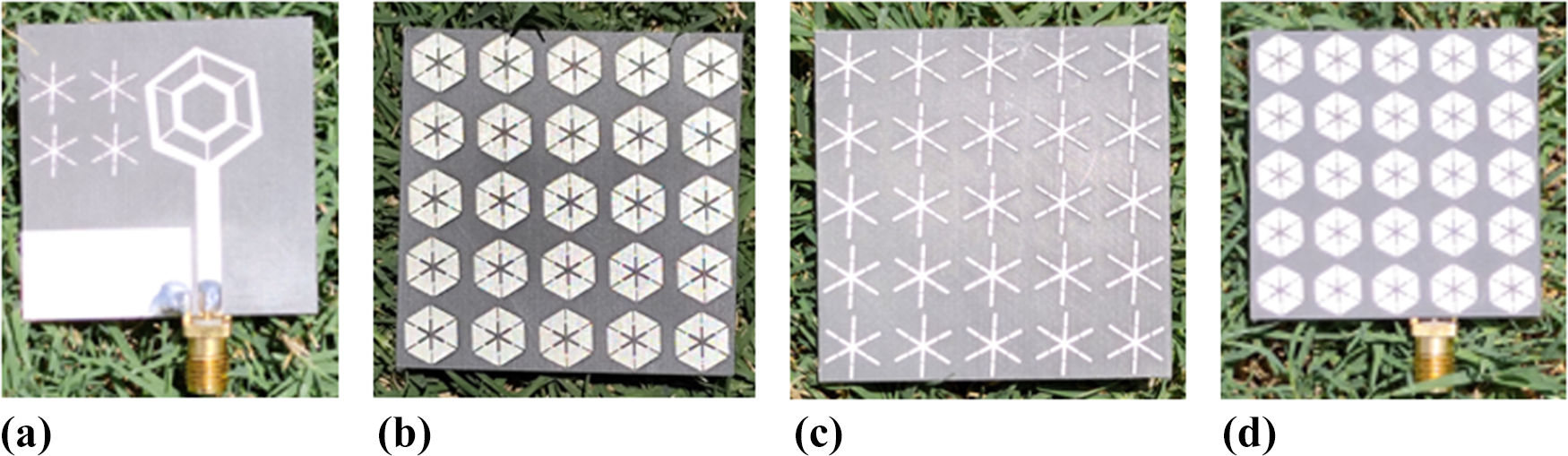
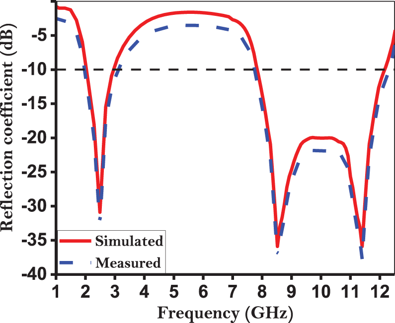
The presented antenna and its MS are fabricated as shown in the Fig. 13 and experimentally validated with and without MS. The Vector Network Analyser (Agilent’s N5230A PNA-L) and JR 24 broadband horn antenna are employed to validate the radiation characteristics of the test antenna. However, some slight variations in the measured radiation characteristics values are noted due to the fabrication precision losses and calibration error. The fabricated prototype’s reflection coefficient responses are plotted in Fig. 14. The presented antenna’s first resonance peak occurs at 2.45 GHz having an impedance bandwidth of 630 MHz and the second resonance peak occurs in X-band having an impedance bandwidth of 4.1 GHz. This shows the capability of the antenna to work for both RFID application 2.45 GHz and X-band radar applications.
Fabricated prototypes: (a) radiating patch, (b) bottom layer of MS, (c) top layer of MS, (d) top view of proposed antenna with MS.

Experimentally validated reflection coefficient (S11).

Also, the axial ratio bandwidth is measured by placing the proposed antenna and a broadband horn antenna in the same orientation initially and with a rotation of 90°. The power received in both the orientations is measured whose difference is considered as the axial ratio in dB. This axial ratio measured falls within the first resonance impedance bandwidth and from the resonance it understands that the presented antenna is CP at 2.45 GHz. The simulated and measured axial ratio characteristics are illustrated in the Fig. 15.
Simulated and measured result axial ratio (dB).

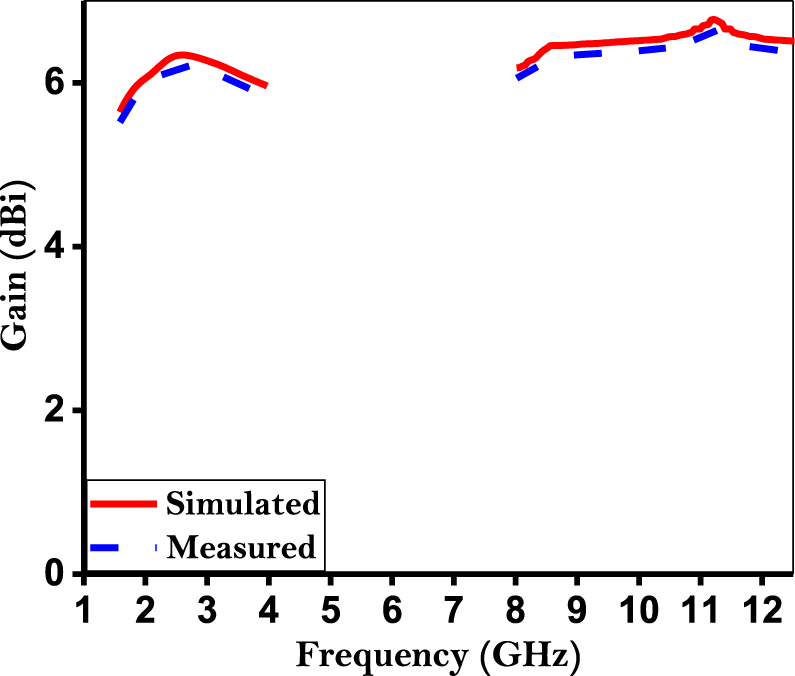
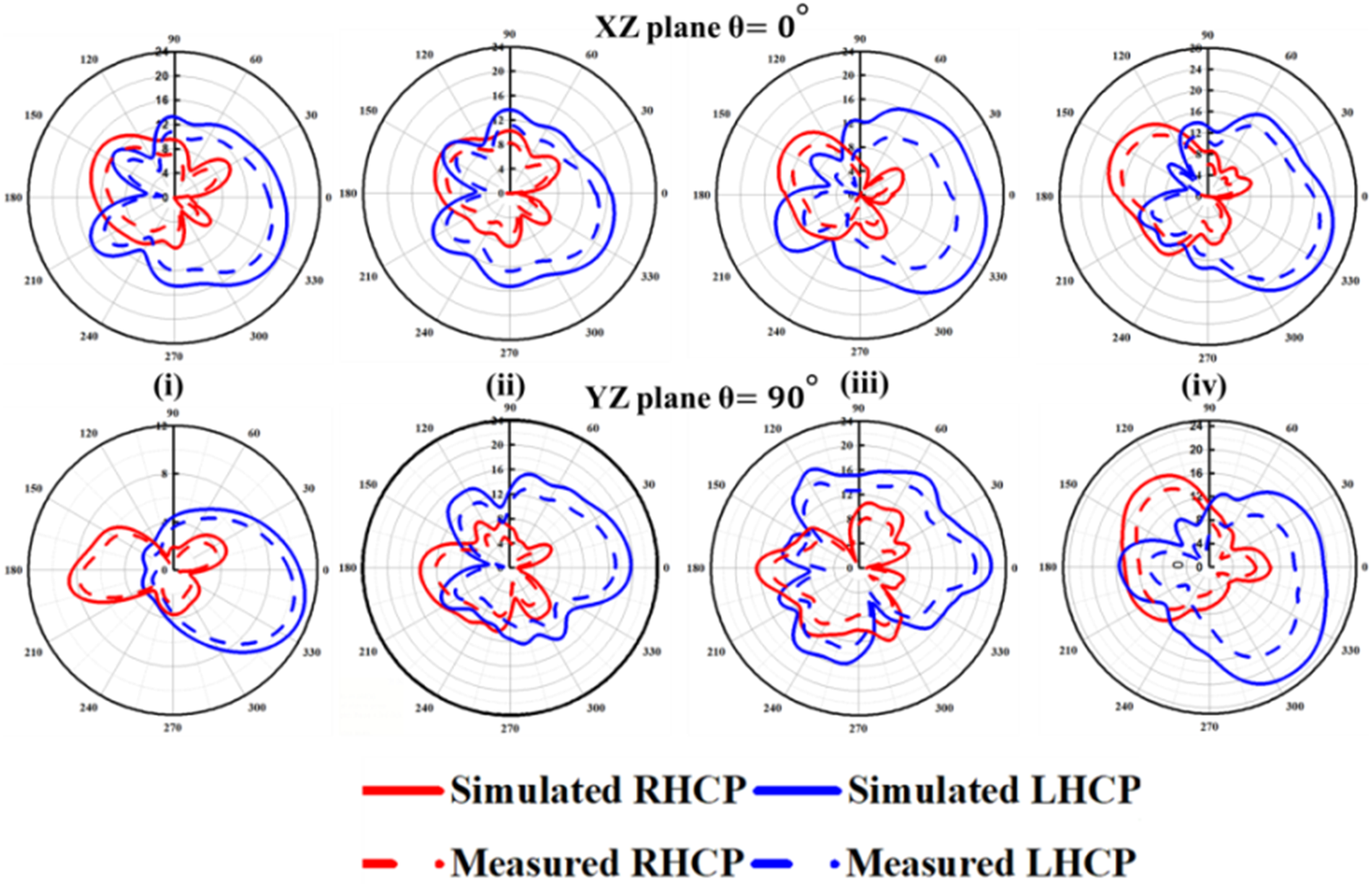
Both the operating band exhibits circular polarization having axial ratio measured as lesser than 3 dB. The measured ARBW is 995 MHz from 2.28 GHz to 3.28 GHz in the first band and 796 MHz from 10.49 GHz to 11.75 GHz in the second band. The measured average gain in the both the bands are 6 dBi as shown in Fig. 16. This enhanced gain is due to the EBG structures present adjacent to the patch and MS above the antenna. The Fig. 17 shows the radiation pattern at 2.45 GHz, 9.1 GHz, 10.9 GHz and 11.5 GHz for both E-plane ( $\theta = {0^\circ })$ and H- planes (
 $\theta = {90^\circ })$. The proposed antenna shows a uniform and unidirectional radiation pattern in bore sight direction.
Simulated and measured gain value.

Experimentally validated radiation characteristics: (i) 2.45 GHz, (ii) 9.1 GHz, (iii) 10 GHz, (iv) 11 GHz.

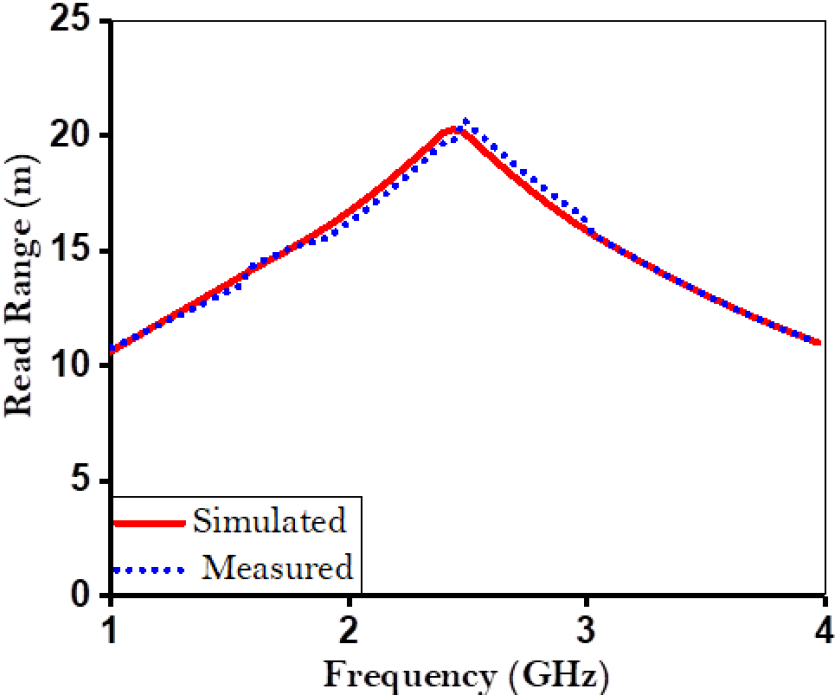
The major parameter that defines the performance of RFID antenna is its read range which is the farthest distance at which the tag’s signal is picked up by the RFID reader. Antenna gain and its orientation are used to calculate this value. Using Friis equation, the read range can be calculated as [Reference Yi and Qu19] in Equation (3).
 \begin{equation}R = {\text{ }}\frac{\lambda }{{4\pi }}{\text{ }}\sqrt {\frac{{{P_t}{G_t}{G_r}{\text{ }}}}{{{P_{th}}}}{\text{ }}} \left\{ {1 - {{\left| {\frac{{{Z_{c{\text{ }}}} - {\text{ }}{Z_a}}}{{{Z_{c{\text{ }}}} + {\text{ }}{Z_a}}}} \right|}^2}} \right\}\end{equation}
where P t is the reader’s power radiated, G t is the gain of the antenna at transmitter side, G r is gain of the antenna at receiver side, and P th is the minimal power needed to activate tag chip. In compliance with the EPC worldwide static test standard, the RFID tag antenna’s read distance is measured by positioning the tag antenna in front of the interrogator antenna on a platform inside the anechoic chamber. The Effective isotropic radiated power (EIRP = P tG t) has an allowed value of 3.3 W in Europe and 4 W in America. The tag antenna used for testing is Alien Higgs IC chip whose P th = − 12 dBm. The read range is calculated for EIRP = 3.3 W and is plotted in Fig. 18. From the graph, the measured read range value is 20 m at 2.4 GHz.
Experimentally validated read range characteristics.

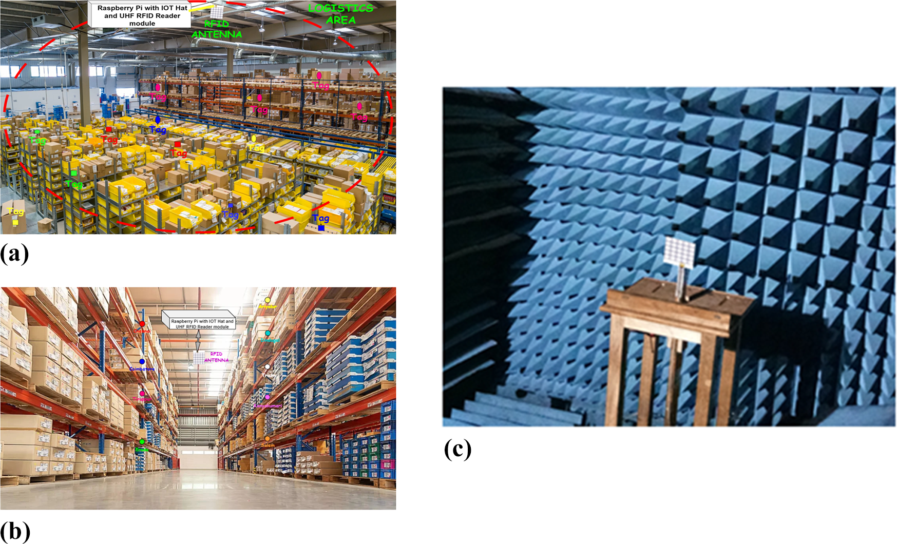
A CP antenna with wide coverage area is necessary for ware house logistic areas since it is very difficult to cover lots of cargos in the entire environment. Also, usage of multiple antennas to cover up the space will increase the cost and interference of the signals. The proposed antenna is demonstrated in two environments such as pharmaceutical ware house and packers and movers ware house as depicted in Fig. 19. The test antenna is connected to a predefined Raspberry Pi IOT Hat and UHF RFID reader module and the total system is placed on the roof of the test area. Since the read range of the antenna is quite higher than the recently stated works, the antenna covers the entire test area and has detected all the tags successfully. The tag used here is of very low cost and replaceable.
Demonstration and measurement of test antenna in (a) warehousing environment, (b) packers and movers, (c) anechoic chamber.

A pharmaceutical warehouse consists of various types of tablets, intravenous solutions, bandages, injection solutions, syringes and syrups. These items are tagged with unique ids, and are marked here with different colors to differentiate the items from one another. The test antenna has read all the tags successfully and listed the items available.
In packers and movers ware house, the parcels from different districts of Tamil Nadu are tagged and placed on the separate racks before taking to delivery. The test antenna with RFID reader module is placed on the roof of the shed and all the tagged items are read and name and date of delivery is listed. Since the test antenna has a read range of 20 m, it has covered the full floor of operation and have listed the entire parcel along with its destination and delivery dates.
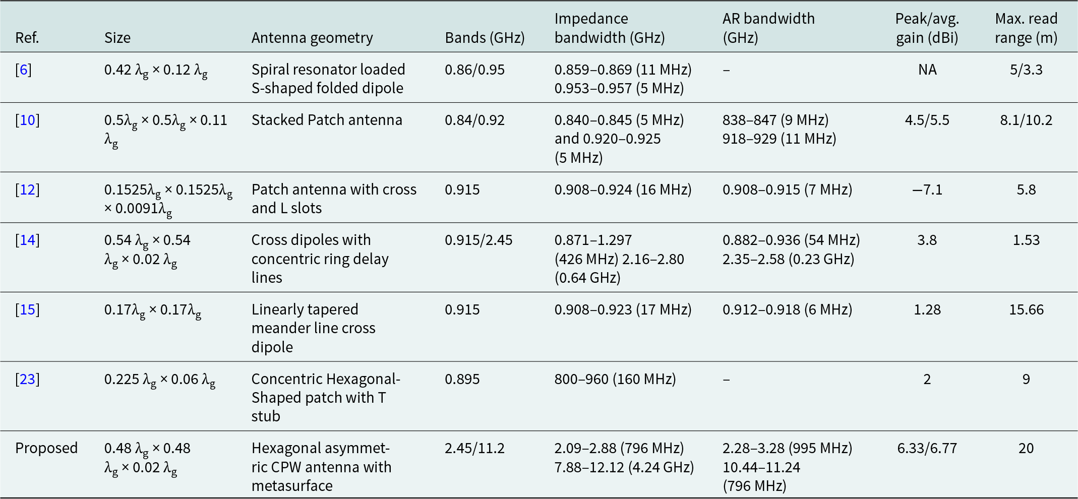
Comparing the work proposed with the recently stated works with respect to impedance bandwidth, gain, axial ratio bandwidth and read range are listed in Table 3. Compared to all the reported works, the presented antenna has enhanced values with respect to all the parameters listed.
Comparison with the recently stated works

Though the size of the antenna in [Reference Wang, She, Han, Fang and Liu10], [Reference Le, Ahmed, Ukkonen and Björninen12], [Reference Lai, Yang and Chen14], and [Reference Bhaskar and Singh15] is less than the proposed antenna, the gain, read range and the bandwidth achieved is quite larger than them.
• High axial ratio bandwidth is achieved without any feed network or lumped elements or external biasing circuits.
• Larger bandwidth enables transmission of larger amount of data reliably. With respect to the average gain and read range, the proposed antenna achieves a higher value compared to all the works stated in the literature.
Conclusion
A unique CP MS based modified CPW fed dual-band antenna of electrical dimension 0.48 λ g × 0.48 λ g × 0.02 λ g is proposed for RFID and X-band applications. The hexagonal radiating patch supported by an asymmetric ground with EBG loaded structure is designed that enhances the impedance bandwidth and circular polarization. Also, the MS with dual layer of complementary unit cell structures is used for enhancement of the average gain that increases the read range for RFID application. The impedance bandwidth from 2.09 GHz to 2.88 GHz (796 MHz) and from 7.88 GHz to 12.12 GHz (4.24 GHz) is achieved. The ARBW of 995 MHz and 796 MHz is achieved in in UHF–RFID and X-band, respectively. Due to its higher impedance bandwidth and ARBW, large amount of data could be transmitted over a wide range of frequency band. In addition to these, a stable radiation characteristic having 6 dBi average gains at both 2.45 GHz and 11.21 GHz is achieved. Higher radiating gain enhances the read range that makes it suitable for applications such as vehicle detection, tracking, IOT systems, inventory tracking, and access control.
Competing interests
The authors declare that they have no known competing financial interests or personal relationships that could have appeared to influence the work reported in this paper.

Bharathi V. was born in Tamil Nadu, India, in 1990. She received her B.E. degree from the Saranathan College of Engineering, Trichy, under Anna University in 2011 and her M.E. in Communication Systems from K. Ramakrishnan College of Engineering, Trichy, under Anna University Chennai in 2013. She is currently a Ph.D. Research Fellow with the Department of Electronics and Communication Engineering, Indian Institute of Information Technology, Tiruchirappalli. Her current research interests include RF, and microwave, antennas, and Frequency Selective Surfaces, Reconfigurable Intelligent Surfaces.

Krishnamurthy Ramanujam was born in Tamil Nadu, India. He received a B.E. degree from St. Peter’s Engineering College, Anna University, Chennai, India, in 2005. The M.E Degree in Telecommunication Engineering and PhD in Optical Networks from the Indian Institute of Science, Bangalore, India, in 2010 and 2020, respectively. He is currently working as an assistant professor at the Department of Electronics and Communication Engineering, Indian Institute of Information Technology, Tiruchirappalli. His research interests include wireless communication, RF, and microwave planar radiating systems.

Parthasarathy Ramanujam received his Bachelor’s Degree in Electronics and Communication Engineering from Anna University, Chennai, India, in 2012; the Masters and Ph.D. degrees in Communication systems and Microwave Filtering Antenna design from Anna University, Chennai, India, in 2014 and 2021, respectively. Currently he is working as an Assistant Professor (Grade II) in the Department of Electronics and Communication Engineering at National Institute of Technology (NIT), Tiruchirappalli, India. Also, he is serving as an Academic Associate dean. He has more than 10 years of teaching and research experience. His research interests include microwave components and circuits, antenna engineering, signal integrity analysis, Frequency Selective Surface (FSS) and solution to EMI problems.