I. INTRODUCTION
Nanostructured metal oxide thin films of e.g., Fe2O3, Al2O3, CuO, ZnO, TiO2, and ZrO2 have attracted considerable attention in recent years due to their versatile properties and promising application possibilities in the fields of electronics, gas sensing, catalysis, photocatalysis, and photovoltaics. Reference Park, Sambasivan, Fischer, Yoon, Misewich and Wong1–Reference Libera, Elam, Sather, Rajh and Dimitrjevic7 These fast emerging application areas put a lot of demands on the fabrication of such metal oxide films, including morphology design, high reproducibility, and possibility to large-scale production. A number of nanopatterning techniques, including scanning probe technique, microcontact printing, and photolithography, have emerged as the predominant methods to fabricate patterns within monolayers of surfactants. Reference Soja and Watson8 However, these methods are limited by the patterning rate and the pattern size, and the scaling-up possibilities of these methods are restricted. A promising and cost-efficient technique to produce large-scale nanopatterned structures on a wide range of substrates is to dip coat a metal oxide sol in the presence of block copolymers. Reference Kuemmel, Allouche, Nicole, Boissière, Laberty, Amenitsch, Sanchez and Grosso9,Reference Järn, Brieler, Kuemmel, Grosso and Lindén10 In this method, evaporation-induced self-assembly (EISA) will arrange the block copolymers into micellar structures that will create nanoperforations or nanocraters in the final TiO2, ZrO2, or Al2O3 networks. Faustini et al. have, for example, used this type of substrates to deposit FePt nanoparticles selectively into the nanoperforations to produce magnetic recording devices. Reference Faustini, Capobianchi, Varvaro and Grosso11 Recently, we have utilized NP-TiO2 films as substrates in the fabrication of nanopatterned polymeric films by inkjet printing. Reference Xu, Ihalainen, Smått, Määttänen, Sund, Wilén and Peltonen12 Inkjet printing has also proven to be a cheap and efficient method for fabrication of electrodes and silica microdot arrays up to millimeter scale. Reference Määttänen, Ihalainen, Pulkkinen, Wang, Tenhu and Peltonen13–Reference Singh, Haverinen, Dhagat and Jabbour16
In this study, we have combined the EISA technique with inkjet printing, to obtain NP-TiO2 surfaces on SiO2 substrates. Comparing to dip-coating and drop-casting methods, inkjet printing provides the advantage of depositing the ink onto target areas, thus enabling the fabrication of microscale arrays and other patterned structures. Thereby, this study explores a novel pathway for high-throughput and cost-effective fabrication of micropatterned NP metal oxide thin films. The results are foreseen to increase the interest toward the development of different devices based on nanostructured metal oxides, such as gas sensors, solar cells, and ultrahigh density data storage units.
II. MATERIALS AND METHODS
A. Fabrication of NP-TiO2
Pieces of silicon wafers (MEMC Electronic Materials, S.p.A.) were treated in a 3 M HNO3 aqueous solution for 24 h after which they were rinsed with distilled water and ethanol and stored in purified (Milli-Q) water. Just before deposition, the wafers were removed from the water and rinsed with ethanol and acetone.
To obtain TiO2 layers with nanoperforations, a PB-b-PEO block copolymer [polybutadiene-b-poly(ethylene oxide), P2325-BdEO, MWPB = 32,000 g/mol, MWPEO = 43,500 g/mol] purchased from Polymer Source Inc. was chosen as the templating agent for its ability to form stable micelles in less polar solvents than water. The concept and preparation steps of initial solution followed the same method as previously described. Reference Kuemmel, Allouche, Nicole, Boissière, Laberty, Amenitsch, Sanchez and Grosso9 Here, the molar ratio between TiCl4, PB-b-PEO, EtOH, THF, and Milli-Q water was 1:0.0006:274:88:23. The mixture was treated by ultrasonication to ensure a homogeneous mixture of inorganic precursor and PB-b-PEO micelles after which 20 vol% of 2-butoxy ethanol (BE) was added and additionally stirred for 1 h. The surface tension of the solution was determined by a SensaDyne PC9000 surface tensiometer (SensaDyne Instrument Division, Mesa, Arizona) at 20 °C. The viscosity of the solution was determined by a Bohlin-CS Rheometer (Bohlin Reologi AB, Lund, Sweden) within the shear rate range 60–200/s at 20 °C. The surface energy of the silicon wafer was determined the same way as reported previously. Reference Xu, Ihalainen, Smått, Määttänen, Sund, Wilén and Peltonen12
The solutions were deposited on cleaned silicon wafers in three different ways: the first one is by dip coating at a constant withdrawal rate of 1.2 mm/s with a relative humidity of less than 20% at ambient temperature (23 ± 2 °C), using a KSV Dip Coater DC (KSV Instruments Ltd., Helsinki, Finland); the second method is by drop casting of 0.1 µL solution directly on the silicon substrate; and the third way is by inkjet printing on the silicon substrate at both ambient temperature and 60 °C, respectively. After deposition, the films were transferred onto a heating plate and calcined at 500 °C for 10 min to decompose the organic components, leaving a thin layer of TiO2 on the substrates.
B. Inkjet printing
Inkjet printing was performed with a Dimatix materials printer (DMP-2800, FUJIFILM Dimatix Inc., Santa Clara, California). The printing was done under ambient conditions without and with plate-heating (60 °C), using either a single nozzle (with a diameter of 21.5 µm) or 16 nozzles open simultaneously. The nominal drop volume was 10 pL, while a 27 ± 3 V firing voltage and a custom waveform were used to ensure optimal droplet formation, with a jetting frequency of 3 kHz. The print areas were designed using the pattern editor included in the Dimatix software. The samples were left to dry at ambient temperature after printing, then calcined at 500 °C for 10 min.
C. Surface characterization
Atomic force microscopy (AFM) images of the films were captured using a Nanoscope V instrument (Veeco Metrology Group, Santa Barbara, California). All images were recorded in tapping mode under ambient conditions (relative humidity = 23 ± 3%, T = 23 ± 2 °C) using silicon cantilevers (NSG 10, NT-MDT, Russia) with a resonance frequency between 190 and 325 kHz, and a tip radius of 10 nm. All images were analyzed by the Scanning Probe Image Processor software, SPIP 5.1.3 (Image Metrology, Denmark), and the following topographical parameters were used for describing the analyzed surfaces; the nearest neighbor distance (NND) provides the distance between geometric centers of the actual shape and its nearest neighbor; Roundness describes the shape's resemblance to a circle, and it will approach 1.0 the closer the shape resembles a circle; material volume (MV), this is estimated from histogram. The optical microscope images (micrographs) were captured using the optical system coupled to AFM.
Scanning electron microscope (SEM) images were captured by a LEO Gemini 1530 (Oberkochen, Germany) instrument with a thermo scientific ultradry silicon drift detector (Madison, Wisconsin). The acceleration voltage was 2.7 kV, and the magnification of the image corresponds to a Polaroid 545 print with the image size of 8.9 cm × 11.4 cm.
Grazing incidence x-ray diffraction measurements (Bruker AXS D8 Discover instrument, Karlsruhe, Germany) confirmed that the films consisted of crystalline anatase TiO2 (results not shown).
III. RESULTS AND DISCUSSION
A. Ink development and tests to verify the formation of NP-TiO2 films
Previously, NP-TiO2 structures have successfully been prepared by dip coating using a sol containing a solvent mixture of 70 vol% EtOH and 30 vol% THF. Reference Xu, Ihalainen, Smått, Määttänen, Sund, Wilén and Peltonen12 However, this solvent mixture is not directly suitable for inkjet printing, due to its low surface tension (23.6 mN/m at 20 °C), low viscosity (0.91 mPa at 20 °C), and especially its low boiling point (74 °C). BE was added as a carrier solvent to the precursor solution to improve jettability. The characteristics of BE are as follows: surface tension: 27.4 mN/m at 20 °C, viscosity: 2.9 mPa at 20 °C, and boiling point: 171 °C. It was experimentally determined that up to 20 vol% of BE can be added to the 70:30 vol% EtOH/THF solution without altering the solution transparency and stability. The parameters of the solution relating to inkjet printing are discussed later.
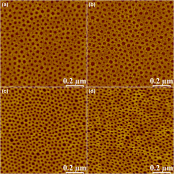
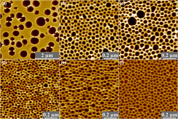
Dip-coated films were prepared using precursor solutions mixed with different volume ratios of BE to examine if the addition of BE would influence the nanostructure of the TiO2 films. Figure 1 shows AFM topographs of dip-coated TiO2 films on a silicon wafer prepared from solutions (a) without BE, (b) with 5 vol% BE, and (c) with 20 vol% BE. NP-TiO2 films with typical perforation morphology were observed for all the samples, and the addition of BE did not have any significant effect on the spherical shape (roundness) of the perforations. However, a more close-packed perforation structure was observed when 20 vol% BE was added. Similar results have been reported by Kuemmel et al., who pointed out that the solubility of PB-b-PEO can be improved by using solvents with low polarity [log Pow for BE is 0.83 (Ref. Reference Hansch, Leo and Hoekman17) and for EtOH it is −0.31 (Ref. Reference Mckarns, Hansch, Caldwell, Morgan, Moore and Doolittle18)], as smaller micelles with higher curvatures can be more accommodated by a solvation system with higher dissolution capacity. Reference Kuemmel, Allouche, Nicole, Boissière, Laberty, Amenitsch, Sanchez and Grosso9 The withdrawal speed (u) used in our dip-coating tests was fixed at 1.2 mm/s, which lies within the “draining regime” as defined by Faustini et al. Reference Faustini, Louis, Albouy, Kuemmel and Grosso19 In this range, the thickness of the liquid film (h S) is determined by the viscous drag, and the wetting properties of the liquid on the substrate surface can be expressed by the Landau–Levich equation, Reference Landau and Levich20 where ηs, γs, and ρs are the viscosity, surface tension, and density of the dipping solution, while g is the standard gravity.
 $${h_{\rm{S}}} = {{0.94\eta _{\rm{S}}^{{2 \mathord{\left/ {\vphantom {2 3}} \right. \kern-\nulldelimiterspace} 3}}} \over {\gamma _{\rm{S}}^{1/6}{{\left( {{\rho _{\rm{S}}}g} \right)}^{1/2}}}}{u^{2/3}}\quad .$$
AFM images of dip-coated structures using (a) unmodified precursor solution, (b) ink with 5 vol% BE, (c) ink with 20 vol% BE, and (d) drop-cast ink with 20 vol% BE. The dark–light height scale corresponds to 10 nm.

As the thickness of the film can be calculated, the MV on the dipping area can then be estimated.
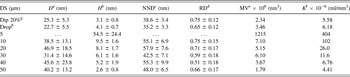
Drop casting was also tested as a dispensing method for a precursor solution with 20 vol% of BE to examine if hydrodynamic conditions (spreading and drying of solvents) more similar to inkjet printing would affect the nanostructure of TiO2 films. Figure 1(d) shows that a NP structure was also obtained by drop casting (i.e., by placing a 0.1 µL droplet of solution on the substrate by a microsyringe). However, compared to the dip-coated film with 20 vol% of BE [Fig. 1(c)], the perforations were smaller and deeper, leading to higher MV values (Table I). The thicker and a more tightly packed film morphology compared to the dip-coated film may result from a limited spreading of the solution due to contact line pinning, Reference Deegan, Bakajin, Dupont, Huber, Nagel and Witten21 which leads to a higher amount of material per area.
Morphological parameters obtained from AFM image analysis of NP-TiO2 films prepared by dip coating, drop casting, and inkjet printing at ambient temperature.

a Measured mean perforation diameter (D).
b Measured mean perforation height from histogram (H).
c Nearest neighbor distance (NND).
d Roundness (RD).
e Material volume (MV).
f Printed volume/area (K, the nominal drop volume was 10 pL).
g Dip coating with 20 vol% BE and
h Drop casting with 0.1 µL ink.
The aforementioned results show that BE can be used as an additive for ink development without influencing the NP structure of the fabricated TiO2 films. The ink containing 20 vol% BE in EtOH/THF (70:30 vol%) was chosen for further printing tests in the following sections as it showed the best jettability with rapid droplet formation without satellite droplets and extensive tail development. The characteristics of this ink were as follows: density: 0.83 g/mL (at 20 °C), surface tension: 24.7 mN/m, and viscosity: 4.10 mPa (at 20 °C). This yielded a Z-value (the inverse Ohnesorge number) of 5.3, further predicting a good printability. Reference Kuscer, Stavber, Trefalt and Kosec22
B. Inkjet printing of individual droplets
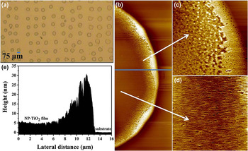
Printing of separate droplets of the precursor ink was conducted to study the droplet spreading and material distribution within the individual droplet. Figure 2(a) shows an optical micrograph of an array of ink droplets that were printed on a silicon wafer, dried at ambient temperature, and then calcined. An average droplet diameter (d) was around 75 µm. The diameter of a dispensed droplet can be expressed as d = 12.4V 1/3, where V is the volume of droplet. Reference Martin, Hutchings, Hutchings and Martin23 For the nominal 10 pL droplet volume, the minimum dispensed droplet diameter would be 26.7 µm. This indicates considerable lateral spreading of the droplet upon impact, which is quite expected due to the large difference between the surface energy of SiO2 substrate (65 mJ/m2) and the surface tension of the ink (24.7 mN/m). The droplet diameter decreased to 65 µm when a temperature of 60 °C was applied to the substrate via a heating plate during printing. The enhanced evaporation by e.g., substrate heating can aggravate contact line pinning by increasing the amount of additional solid material present at the contact line, thus leading to a smaller droplet diameter.
(a) A microscope image of an inkjet-printed single droplet with DS 150 µm; AFM images of an inkjet-printed single droplet with DS 200 µm: (b) a part of a single printed TiO2 droplet, 40 µm × 15 µm, (c) zoom in on the edge, 5 µm × 5 µm, (d) zoom in on the center, 5 µm × 5 µm, and (e) a line profile from center to the edge, corresponding to the blue line in Fig. 2(b).

Figure 2(b) shows an AFM topographical image of a part of a single-printed TiO2 droplet after calcination. A heterogeneous distribution of material was observed within the droplet, which has a thicker perimeter and a thinner center area. This type of heterogeneity is typically caused by the “coffee stain” effect. The thickness of the calcined droplet decreases significantly from the edge (∼30 nm) to the center (∼5 nm), shown in Fig. 2(e). A similar coffee stain effect was observed for a drop-cast ink droplet (diameter ∼4.5 µm, 0.1 µL of ink) in the optical micrograph showing a clearly darker optical contrast in the drop perimeter compared to the center area [Fig. 3(a)]. This indicates that the coffee stain formation was not scale-dependent but was observed for both micro- and macroscale droplets. The coffee stain formation has been explained by the “capillary flow” theory, reported by Deegan et al. Reference Deegan, Bakajin, Dupont, Huber, Nagel and Witten21 They determined that the liquid evaporation from the edge must be replenished by the liquid from the interior as the contact line of the drying drop is pinned, which finally results in an outward flow carrying the dispersed material to the edge. This corresponds well with a thicker TiO2 film at the edge as shown in Fig. 2(c) and a thinner TiO2 in the center in Fig. 2(d). In Fig. 2(d), elongated TiO2 nanoperforations were observed. Polymeric material is known to stretch and elongate in the nozzle during jetting. Reference Martin, Hutchings, Hutchings and Martin23 It is possible that spherical polymer micelles in the precursor ink are deformed during jetting and do not have time to reform the spherical shape after landing due to the fast drying of the droplet. Reference Dijksman, Pierik, Hutchings and Martin24
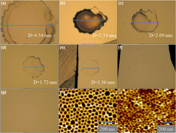
Microscope images of TiO2 structures prepared by (a) drop casting and by inkjet printing with DS, (b) 5 µm, (c) 10 µm, (d) 20 µm, (e) 30 µm, (f) 40 µm, and (g) 50 µm at ambient temperature; AFM images for (h) thinner (thickness = 9.5 nm) and (i) thicker (thickness = 31.4 nm) regions of Fig. 3(c), respectively.

C. Fabrication of NP-TiO2 films by inkjet printing
1. Inkjet printing of TiO2 films at ambient temperature
A square with nominal size of 1 mm × 1 mm was used for the fabrication of TiO2 films by printing. The amount of material was controlled by changing the drop spacing (DS) value within the printed area, a higher DS refers to a larger distance between the printed droplets (in micrometers) and thus a lower amount of ink per unit area, i.e., the amount of droplets is 40,401, 10,201, 2601, 1156, 676, and 441 when the DS value is set to be 5, 10, 20, 30, 40, and 50 µm, respectively. Printing was first conducted using only a single nozzle to keep the reproducibility high. However, as observed in preliminary tests with single droplets [Figs. 2(b)–2(e)], this did not result in NP-TiO2 films with any of the selected DS values. Instead, printing using all the 16 nozzles resulted in the formation of NP-TiO2 structures with varying nanoperforation morphologies. These results are presented and discussed in the following sections. The difference between single and multinozzle printing can most probably be related to the evaporation time of the solvent and the time needed for the PB-b-PEO block copolymer micelles to organize from the elongated structure caused by the jetting to the energetically favorable spherical form. Reference Martin, Hutchings, Hutchings and Martin23 In our study, the coffee stain effect of each single droplet vanished when the droplets were partially overlapping, resulting in a relatively homogeneous thin film in the center parts of each printing area. However, the coffee stain effect could not be avoided at the millimeter length scale. Figs. 3 and 4 show optical micrographs and the corresponding AFM topographs of typical printed area with different DS values.
AFM images of NP-TiO2 films prepared by inkjet printing with DS (a) 5 µm, (b) 10 µm, (c) 20 µm, (d) 30 µm, (e) 40 µm, and (f) 50 µm at ambient temperature. The height scale in (a) is 120 nm and in (b)–(f) is 10 nm.

The shape, size, and optical homogeneity of the printed areas were affected by the DS value, resulting in a more homogeneous production of the designed area with decreasing ink volume per unit area (Fig. 3). Identifying the printed area from an optical micrograph became progressively more difficult with decreasing ink amount, and no areas could be detected with DS 40 and 50 µm. The areas printed with DS values of 30 µm or smaller showed extensive bulging and spreading behavior with wavy and curved edges, and greater variation in optical contrast within the area. Bulging refers to an unstable printing point, where the contact angle of the ink at the substrate is larger than the advancing contact angle. Reference Duineveld25 Within a suitable DS range, the bulging effect Reference Soltman and Subramanian26,Reference Stringer and Derby27 enables the formation of a continuous thin liquid layer on the substrate, preventing the formation of either individual droplets or a stacked coin-type structure. Moon et al. reported recently Reference Moon, Kang, Lee, Kang, Cho, Hwang and Moon28 that stable printing can be obtained, and irregular bulge formation can in most cases be prevented when the DS values were 0.5–0.6 times the droplet diameter. For the average droplet diameter of about 75 µm observed here, this would correspond to a DS of 37.5–40 µm. This fits nicely with the observed results, showing that with a DS of 40 and 50 µm, no bulging was observed [Figs. 3(f) and 3(g)]. The darker contrast in the optical micrographs is related to thicker parts of the films, and these regions generally showed more poorly defined nanoperforation morphology. On the other hand, AFM images captured from thinner regions had clearly defined nanoperforation morphologies and good reproducibility. Figures 3(h) and 3(i) show AFM topographs captured from a thinner (lighter contrast) and a thicker (darker contrast) region of the TiO2 structure depicted in Fig. 3(c). The maximum height differences in the NP structure in these two parts are 9.5 and 31.4 nm, respectively. However, it should be noted that the thicker part could consist of several micelle-templated layers, and in that case, the surface of the SiO2 substrate cannot be probed by the AFM tip, which makes the actual film thickness estimation difficult.
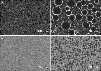
Figure 4 shows AFM topographs captured at the thin part of the printed areas shown in Fig. 3. Similar structures of Figs. 4(a) and 4(d) are also supported by SEM images in Fig. 5. Table I lists the morphological parameters obtained from the respective AFM images. Excluding the TiO2 film printed with DS 5 µm, all the samples show a quite uniform NP structure. The average height (H) of the nanoperforations increases with increasing amount of ink deposited per area (K). When comparing the H values of the samples with approximately similar K values, it is evident that the deposition method did not have a significant effect on the perforation height. However, printing resulted in a larger perforation diameter (D) and less close-packed perforation morphology compared to dip-coated or drop-cast TiO2 films. In addition to the height, the diameter, the packing (NND) and the roundness were also affected by the K value and thus the amount of material and the evaporation time of the carrier solution.
SEM images of TiO2 structures prepared by inkjet printing with different DS values at ambient temperature. (a) and (b) show the DS 5 µm film at magnifications of 5 and 25k, respectively; (c) and (d) show the DS 30 µm film at magnifications of 25 and 50k, respectively.

When excessive precursor amounts were printed with DS 5 µm, the TiO2 film consisting of hierarchical surface structure with microsized and nanosized perforations were confirmed by both AFM [Fig. 4(a)] and SEM [Figs. 5(a) and 5(b)]. In addition, the microsized perforations are significantly deeper than the nanosized perforations typically observed for the printed TiO2 films (Table I). The formation of micrometer-sized perforations is related to the spinodal decomposition mechanism, which has earlier been shown for dip-coated films. Reference Kajihara and Yao29,Reference Fuertes and Soler-Illia30 We believe that a similar structure can be achieved by phase separation between the solvent and block copolymer/TiO2 species at the point of gelation.
2. Inkjet printing of TiO2 with substrate heating
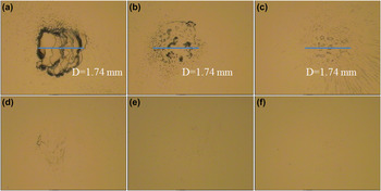
Previous results in Sec. III. C. 1 indicated that the evaporation time had an effect on macroscopic heterogeneity of the printed areas and the morphology of TiO2 films. To examine this further, the effect of evaporation time on print quality and TiO2 morphology was studied by heating the substrate during printing (using multiple nozzles). The heating plate temperature was set to 60 °C. Figure 6 shows that areas printed using a small DS value (i.e., 5–20 µm) appear to be more heterogeneous compared to the ones printed at ambient temperature. However, bulging and coffee ring effects at the edge of the areas have decreased, and the areas have approximately the same diameter. On the other hand, with larger DS values (30–50 µm), substrate heating generated a better distribution of the ink on the surface, and the areas became less visible.
Microscope images of TiO2 structures prepared by inkjet printing with DS (a) 5 µm, (b) 10 µm, (c) 20 µm, (d) 30 µm, (e) 40 µm, and (f) 50 µm at 60 °C.

The results suggest that with the jetting frequency used here, the heating of the substrate shifts the printing behavior from the bulging region to the stacked coin region for the films printed with a small DS. Reference Duineveld25,Reference Soltman and Subramanian26 The effect of heating on the film formation can be explained in a similar way as for a film printed with a single nozzle without heating, i.e., the evaporation time for a single droplet (even with multinozzle printing) is faster than the jetting frequency, and each droplet will dry individually. This results in a heterogeneous macroscopic morphology after drying. The decreased coffee stain effect can be also explained by the increased temperature. It has previously been shown that the Marangoni flow can be initiated by the temperature increase in organic solvents, which leads to a greater deposition of the solute to the center region than the perimeter. Reference Hu and Larson31 However, the opposite temperature effect has been observed for aqueous solutions (i.e., an enhanced coffee stain effect). Reference Duineveld25
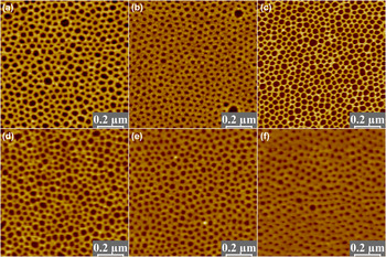
Figure 7 shows AFM topographs captured at the thin part of the corresponding printing areas shown in Fig. 6. Table II lists the morphological parameters obtained from the respective AFM images. All the samples printed using substrate heating show the typical perforation morphology. Most of the studied parameters are not affected by the amount of ink per area (or DS) and are very similar to those of the dip-coated films both without and with BE. The H values are fluctuating close to the values observed for the dip-coated and drop-cast films. These results further indicate that the printing conditions, which involve less bulging and faster drying, are more optimal for formation of NP-TiO2 films. However, to improve the macroscopic homogeneity, a careful optimization of the jetting frequency, temperature, and DS has to be done.
AFM images of NP-TiO2 films prepared by inkjet printing with DS (a) 5 µm, (b) 10 µm, (c) 20 µm, (d) 30 µm, (e) 40 µm, and (f) 50 µm at 60 °C. The height scale is 10 nm.

Morphological parameters obtained from AFM image analysis of inkjet-printed NP-TiO2 films prepared at 60 °C.

a Measured mean perforation diameter (D).
b Measured mean perforation height from histogram (H).
c Nearest neighbor distance (NND).
d Roundness (RD).
e Material volume (MV).
f Printed volume/area (K, the nominal drop volume was 10 pL).
IV. CONCLUSIONS
In summary, we demonstrate herein a high throughput fabrication method of NP-TiO2 structures by inkjet printing. This method enables the fabrication of micropatterned structures of NP-TiO2 in comparison to previously published dip-coated NP-TiO2 films, which cover a large area on the substrate. We have shown that the addition of a solvent with high viscosity and high-boiling point (2-butoxyethanol) to the precursor solution did not affect the formation of the NP-TiO2 structure, but it clearly improved the printability of the precursor solution. It was further demonstrated that with a large droplet spacing and small amount of ink (e.g., DS 200 µm), individual ink droplets could be formed on the substrate, where elongated TiO2 nanoperforations were observed in the center of the calcined droplet. On the other hand, with DS in the range of 10–50 µm, a NP-TiO2 structure was obtained at both ambient temperature and 60 °C. Compared to ambient temperature, printing at 60 °C provided a narrower height distribution of about 5 nm due to the fast evaporation of the solvents in the inks. Especially for DS 40 and 50 µm, very homogeneous, millimeter-sized NP-TiO2 areas could be obtained. However, for DS values below 30 µm, additional macroscopic heterogeneities were observed, resulting from “coffee stain”- or “stacked coin”-related effects. Although it is possible to obtain patches with the well-defined NP-TiO2 structure at such low DS values as well, a lot of the TiO2 and block copolymer material will be wasted inside the ill-defined heterogeneities. Thus, using the printing settings with a DS of 40 or 50 µm resulted in an optimal liquid film thickness that produces a thin and homogeneous TiO2 structure similar to the dip-coated samples. The main advantage of inkjet printing is that one can deposit the inks onto the target area with high-print resolution, thus providing great possibilities for patterning NP-TiO2 on the surface according to the needs of the application. Furthermore, we believe that it is also possible to utilize inkjet printing for other types of NP metal oxide thin films, including ZrO2 and Al2O3, on various substrates. This opens up new avenues for the fabrication of gas sensors, solar cells, and ultrahigh density data storage devices.
ACKNOWLEDGMENTS
The Academy of Finland is greatly acknowledged for the financial support through the project 118266 (QX). Magnus Ehrnrooth Foundation and Stiftelsens för Åbo Akademi forskningsinstitut are also acknowledged for additional financial support (QX).