I. INTRODUCTION
Microwave multiplexers are widely used in space and terrestrial communication systems, and special attention is paid to reduce their size and weight.
Traditionally, microwave multiplexers include several elements such as power dividers, circulators or manifold networks for connecting channel filters [Reference Rhodes and Levy1–Reference Kudsia, Cameron and Tang3]. These additional elements allow a separate design of each channel; however, they contribute to increased size and weight and also have a non-negligible impact on electrical performances (insertion loss, power handling, etc.). In the case of manifold multiplexing, optimization of waveguide elements is required to meet the electrical specifications, and this could be computationally extensive when a high number of channels are considered.
To suppress waveguide junctions in multiplexing networks, compact microwave multiplexers exclusively composed of coupled resonators have been introduced [Reference Ezzeddine, Bila, Verdeyme, Seyfert and Pacaud4–Reference Loras-Gonzalez, Sobrino-Arias, Hidalgo-Carpintero, García-Lampérez and Salazar-Palma10]. This new concept allows a large reduction of size and weight compared to conventional microwave multiplexers. Moreover, compact multiplexers offer additional flexibility compared to other multiplexing networks, since coupling between different channels is now possible [Reference Garcia-Lamperez, Salazar-Palma and Sarkar8].
For designing such compact multiplexers, analytical methods for evaluating characteristic polynomials and generalized coupling matrix of microwave multiport networks have been developed. These methods have been validated and several prototypes of diplexers and triplexers have been manufactured using a variety of technologies [Reference Macchiarella and Tamiazzo6–Reference Loras-Gonzalez, Sobrino-Arias, Hidalgo-Carpintero, García-Lampérez and Salazar-Palma10], but up to our knowledge, only using single-mode resonators.
In this paper, for more compactness, a dual-mode implementation of microwave diplexers and triplexers is proposed. These devices are designed to be consistent with an output multiplexer for satellite payload. Consequently, for a matter of power handling and quality factor, empty cavities working on their TE113 dual mode are used for their implementation.
Two topologies of compact diplexers are proposed and compared to a manifold diplexer in terms of electrical performance and integration. Compared to our previous works [Reference Ezzeddine, Bila, Verdeyme, Seyfert and Pacaud4, Reference Ezzeddine5], the current paper provides measurements on a compact diplexer prototype and the design of a compact triplexer to generalize the approach.
II. MANIFOLD DIPLEXER
For reference, a manifold diplexer consisting of two dual-mode cavity filters coupled with waveguide sections has been designed. The electrical specifications for each channel are: a return loss of 20 dB and an out-of-band rejection of 8 dB at ±45 MHz and 18 dB at ±55 MHz from the center frequency. The two 72-MHz channels are centered at 10.741 and 10.821 GHz, respectively.
To reach the electrical specifications, each channel requires a five-pole quasi-elliptic function with two transmission zeros at ω 1,2 = ±1.33 rad/s.
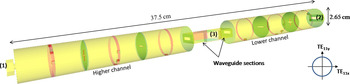
For dimensioning such a structure, we applied a classical approach that consists of designing channel filters independently, then optimizing the whole diplexer structure. The manifold diplexer is shown in Fig. 1 and the optimized electromagnetic (EM) response is shown in Fig. 2. The insertion loss is found to be 0.28 dB and the diplexer structure is contained in parallelepiped occupying 37.5 × 2.65 × 2.65 = 263 cm3.
EM model of the manifold diplexer.

Optimized EM response of the manifold diplexer.

III. COMPACT DIPLEXER: FIRST TOPOLOGY
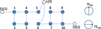
The first topology of compact diplexer is shown in Fig. 3. This topology is directly derived from the classical architecture of the microwave diplexer. Indeed, the structure consists of two independent paths (resonators 1–5 and resonators 6–10), and the common port L excites the two paths simultaneously.
First coupling topology for realizing the compact diplexer.

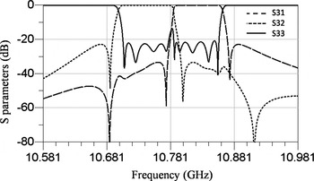
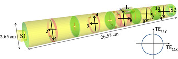
To calculate the generalized coupling matrix of the diplexer, we did not calculate the characteristic polynomials as in [Reference Macchiarella and Tamiazzo6, Reference Macchiarella and Tamiazzo7], but we directly optimized the coupling matrix with a circuit software. After optimization, we obtained a transfer function as shown in Fig. 4. The generalized coupling matrix, given in equation (1) is normalized with respect to a center frequency of 10.781 GHz and a passband of 72 MHz covering the two passbands of the diplexer. For implementing this topology in dual-mode cavities, we used the same approach as for classical filters [Reference Atia and Williams11]. The EM structure corresponding to the first topology is shown in Fig. 5. For feeding simultaneously resonators 5 and 6 by the common port L, a coupling iris was placed at 45° from the two orthogonal polarizations (TE11x and TE11y). To avoid deep penetration of the screws into the cavity and to keep the symmetry, we used diametrically opposed screws in the middle cavity. Moreover, the screws and the iris are not placed on the same maxima of electric field (TE113) to reduce the sensitivity of the structure.

Optimized circuit response for the first coupling topology.

EM structure of compact diplexer with the first coupling topology.

For dimensioning the structure shown in Fig. 5, we divided it into three parts. The two channel paths and the common center cavity were designed separately and the whole structure was finally slightly optimized.
A) Lower channel path
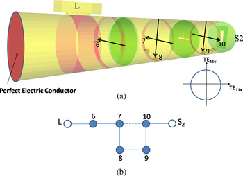
Considering one-half of the structure closed by a perfect electric conductor (PEC), and, placing the excitation so as to excite only one polarization as shown in Fig. 6, we were able to tune the lower channel segment iteratively by using a coupling matrix identification approach [Reference Bila12, Reference Seyfert and Bila13]. The EM response was identified to be a transfer function with five poles and two transmission zeros and the corresponding coupling matrix was compared to the second half of the generalized coupling matrix.
(a) EM structure for dimensioning the lower channel path and (b) equivalent coupling topology.

B) Higher channel path
The same segment was used to tune the higher channel. In this case, the dimensions were calculated by comparing the extracted coupling matrix to the first half of the generalized coupling matrix.
C) Common cavity
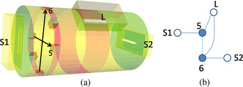
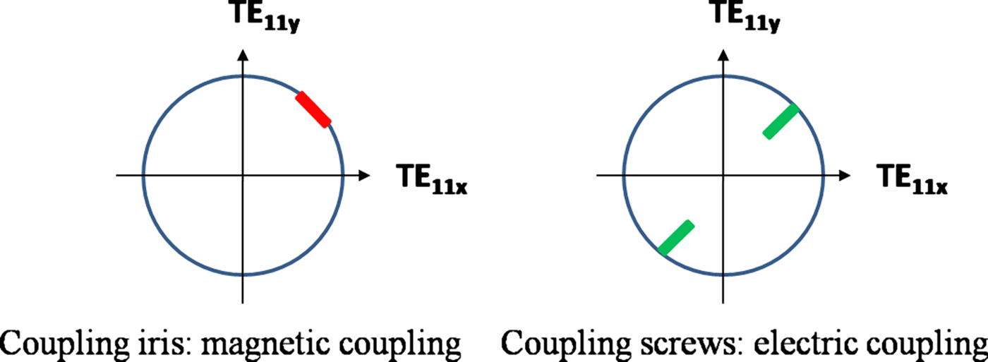
To precisely tune the structure, a pre-dimensioning of the common (center) cavity with the excitation placed at 45° from the two polarizations was necessary. The considered segment in this case is described in Fig. 7(a). The dimensions of this segment were initialized by identification of the equivalent circuit presented in Fig. 7(b), where resonators 5 and 6 represent the two orthogonal polarizations in the common cavity. The coupling between these two polarizations has to be null; however, the feeding element (coupling iris) placed at 45° creates inevitably an undesirable coupling. To balance this magnetic coupling, we introduced additional screws placed also at 45° from the two polarizations as shown in Fig. 8. The electric coupling realized with the additional screws cancels the undesirable coupling. The other (desirable) couplings in this segment are adjusted by tuning the iris length and the other screws.
(a) EM structure for dimensioning the common cavity and (b) equivalent coupling topology.

Compensation of the parasitic coupling due to excitation.

D) Compact diplexer
Once the three segments were dimensioned, the whole structure was analyzed. The response shown in Fig. 9(a) is close to the desired one; however, a fine tuning of the whole structure remained necessary to satisfy the specifications, especially in terms of return loss. The optimized response of the compact diplexer is shown in Fig. 9(b). The insertion loss is 0.27 dB and the structure occupies 26.53 × 2.65 × 2.65 = 186 cm3.
EM response of the first compact diplexer: (a) before fine tuning and (b) after fine tuning.

Compared to our previous work [Reference Ezzeddine, Bila, Verdeyme, Seyfert and Pacaud4], the common cavity has been pre-dimensioned for more accurate design and, thanks to additional tuning screws; the spurious resonances have been eliminated by improving the overall performance of this compact diplexer configuration.
IV. COMPACT DIPLEXER: SECOND TOPOLOGY
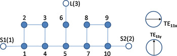
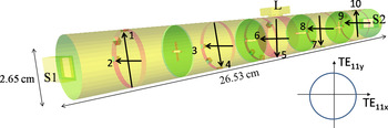
For facilitating the dual-mode implementation, a second topology described in Fig. 10 has been proposed [Reference Ezzeddine, Bila, Verdeyme, Seyfert and Pacaud4]. With this topology, the common port L excites a single resonator. Consequently, the magnetic iris is now placed orthogonal to polarization TE11x as shown in Fig. 11.
Second coupling topology for realizing the compact diplexer.

EM structure of compact diplexer with the second topology.

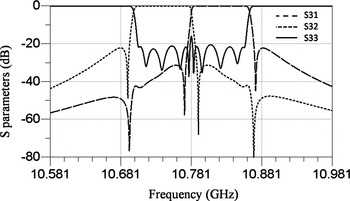
The design begins with the synthesis of the generalized coupling matrix. The coupling matrix given in equation (2) was obtained by circuital optimization and the corresponding responses shown in Fig. 12, satisfies the desired electrical specifications. The coupling matrix is normalized with respect to a center frequency of 10.781 GHz and a passband of 72 MHz. One can note that coupling M 56 is almost double than other couplings. This is due to this particular topology where resonators 5 and 6 are shared by the two paths corresponding to the two passbands; consequently, this coupling covers the whole band of the diplexer (152 MHz). Besides, comparing the circuit responses in Fig. 4 and Fig. 12, one can see that transmission zeros due to channel interactions have disappeared in this configuration. Therefore, the second topology is less attractive in terms of channel isolation and out-of-band rejection.

Optimized circuit response for the second topology.

After this circuital optimization, the diplexer dimensions have to be determined; however, only two segments have to be considered since the center cavity is common to the two paths.
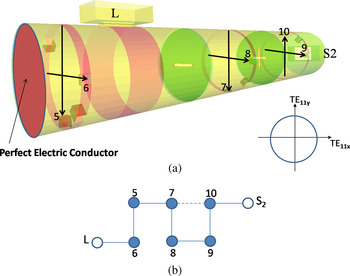
A) Lower channel path
The segment used for initializing the dimensions of the lower channel is shown in Fig. 13. This segment is built with one-half of the whole structure and the other half is replaced by a PEC. The segment was tuned by coupling matrix identification [Reference Bila12, Reference Seyfert and Bila13] and the response was identified to be a transfer function with six poles and two transmission zeros, comparing the corresponding coupling matrix to the second half of the generalized coupling matrix.
(a) EM structure for dimensioning the lower channel path (second topology) and (b) equivalent coupling topology.

B) Higher channel path
The same segment was used to tune the higher channel. In this case, the dimensions were adjusted with respect to the first half of the generalized coupling matrix.
C) Compact diplexer
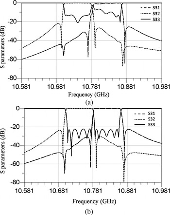
Finally, a global optimization of the whole structure was necessary to satisfy the specifications especially in terms of return loss. The EM response of the diplexer in this topology is shown in Fig. 14 before and after optimization. In this configuration, insertion loss is also found to be 0.27 dB and the volume occupation is similar to our previous topology (186 cm3).
EM optimized response of the second compact diplexer: (a) before fine tuning and (b) after fine tuning.

V. EXPERIMENTS
For validating the design of compact diplexers in dual-mode cavities, a hardware prototype was fabricated as shown in Fig. 15. The second topology was preferred for facilitating implementation and tuning. The cavities are silver plated for increasing the electrical conductivity.
Photography of the fabricated diplexer.

The two channel paths were separately preset using coupling matrix identification to facilitate the tuning. The whole diplexer is then assembled and finely tuned. The measured response displayed in Fig. 16 is in good accordance with the simulation. Insertion losses are 0.38 dB in the lower channel and 0.36 dB in the higher channel.
Measured (solid line) and simulated (dashed line) diplexer response.

VI. COMPACT TRIPLEXER
For extending the approach to more than three ports, a compact triplexer with contiguous channels is proposed. The three 72-MHz channels are centered at 10.701, 10.781, and 10.861 GHz, respectively. The return loss is expected to be 18 dB in each channel, and the out-of-band rejection is at least 15 dB at ±58 MHz from the center frequency. The triplexer is synthesized through circuit optimization. Four pole channels are necessary for attaining the out-of-band rejections and two transmission zeros are added in the middle channel for increasing isolation between channels.
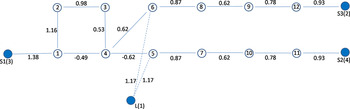
Fig. 17 shows the optimized coupling topology. Synthesized coupling values are reported in the coupling diagram and self-couplings are given in the figure caption. All these couplings are normalized with respect to a center frequency of 10.781 GHz and a passband of 72 MHz. One can distinguish easily the three channel paths: the lower channel path is composed of resonators 6, 8, 9, and 12; the higher channel path is composed of resonators 5, 7, 10, and 11; and the middle channel path is composed of resonators 1, 2, 3, and 4. The latter channel requires a coupling between resonators 1 and 4 to realize the pair of transmission zeros. Moreover, one can remark that couplings and self-couplings are symmetrically arranged because of the symmetry in the electrical specifications.
Coupling topology for realizing the compact triplexer. M 11 = M 22 = M 33 = M 44 = 0, M 55 = −M 66 = 2.32, M 77 = −M 88 = 2.25, M 99 = −M 1010 = −2.24, and M 1111 = −M 1212 = 2.23.

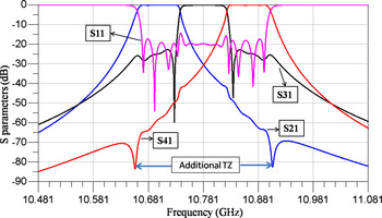
The corresponding transfer function is shown in Fig. 18. Additional transmission zeros are observed in the passbands of opposite channels, improving the isolation between them. The location of such incomplete transmission zeros depends on couplings between resonators of lower and higher channels (M 56, M 78, etc.).
Optimized circuit response for the compact triplexer.

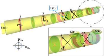
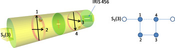
The implementation in dual-mode cavities is shown in Fig. 19. To couple resonator 4 to resonators 5 and 6, dual-mode polarizations were rotated by 45° with respect to polarizations TE11x and TE11y. For simultaneously feeding resonators 5 and 6 by the common port L, a coupling iris was placed at 45° from the two polarizations 5 and 6 are depicted in Fig. 19.
EM model of the compact triplexer.

For dimensioning the structure, each channel path has been separately designed. Moreover, for obtaining an accurate dimensioning, an additional segment was used to precisely evaluate couplings between resonators 4, 5, and 6. Finally, the whole structure was finally optimized.
A) Higher channel path
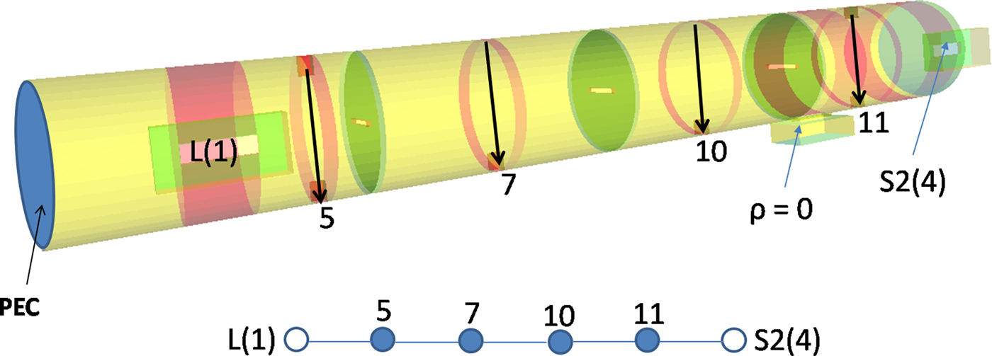
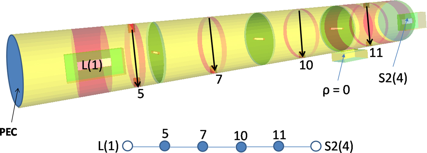
The segment used for initializing dimensions of the higher channel path is shown in Fig. 20. This segment corresponds to the right half of the whole structure. The two first cavities were replaced by a PEC. Moreover, the coupling iris of common port L is placed so as to excite only one polarization. The port corresponding to the lower channel path is replaced by a matched load condition (ρ = 0).
EM structure for dimensioning the higher channel path and its equivalent coupling topology.
B) Lower channel path
The same segment was used to tune the lower channel. In this case, the lower channel port S3(2) is considered, and tuning screws are dimensioned for adjusting resonant frequencies.
C) Segment used for tuning couplings between resonators 4, 5, and 6
As for the first topology of compact diplexers, a pre-dimensioning of the common cavity with the excitation placed at 45° from the two polarizations (5 and 6) was necessary. Moreover, for initializing precisely dimensions of the iris realizing couplings M 45 and M 46, the segment described in Fig. 21 was considered.
EM structure for dimensioning the middle cavity and its equivalent coupling topology.

D) Middle channel path
The segment used for dimensioning the middle channel is shown in Fig. 22. This segment is built with the two first cavities.
EM structure for dimensioning the middle channel path and its equivalent coupling topology.

All these segments were tuned by coupling matrix identification [Reference Bila12, Reference Seyfert and Bila13]. For each segment, the response was identified to be the transfer function corresponding to its equivalent coupling topology. The identified couplings were compared to the corresponding desired ones shown in Fig. 17.
E) Compact triplexer
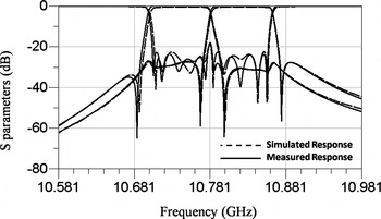
Once the segments have been dimensioned, the whole structure was analyzed. The response after the segmentation stage is close to the desired one; however, a fine tuning of the whole structure remained necessary. The optimized response, compared to the theoretical one, is shown in Fig. 23. One can observe that additional transmission zeros have disappeared on the simulated response. This is due to weak couplings between resonators of lower and higher channels (M 56, M 78, etc.).
Simulated (solid line) and theoretical (dashed line) triplexer response.

VII. CONCLUSION
In this paper, several topologies for realizing compact microwave diplexers and triplexers in dual-mode cavities have been proposed. These devices are exclusively composed of coupled resonators and their designs have been described in detail. The approach has also been illustrated by a fabricated prototype.
The first compact diplexer, which is inspired by classical diplexer architecture, is more attractive in terms of out-of-band rejection since it presents an increased selectivity. Nevertheless, it requires a careful design for dimensioning properly the cavity supporting the common port.
The second topology excites a single resonator at the common port. Implementing this configuration is more comfortable; however, the selectivity is reduced compared to the first topology. Measurements of a hardware prototype are in good accord with the theoretical design.
The two first topologies have been compared with a manifold diplexer. The diplexers allow reducing volume occupation by 29%, whereas electrical performances in terms of insertion loss and out-of-band rejection (first topology) are comparable.
Finally, the approach was extended to four-port devices for realizing compact triplexers.
 Hussein Ezzeddine was born in Deir Kanoun, Lebanon, in August 1985. He received his Engineer degree from the National School of Engineers of Limoges, France, in 2008, and is currently working toward the Ph.D. degree in high-frequency electronics and opto-electronics at the University of Limoges, Limoges, France. He is currently with the XLIM, University of Limoges. His research interests include synthesis methods based on computer-aided techniques for the design and optimization of microwave components and circuits for space applications.
 Stéphane Bila was born in Paris, France, in September 1973. He received a Ph.D. degree from the University of Limoges, Limoges, France, in 1999. He then held a post-doctoral position for one year with the French Space Agency (CNES), Toulouse, France. In 2000, he became a Researcher with the National Centre for Scientific Research (CNRS) and joined IRCOM (now XLIM), Limoges, France. His research interests include numerical modeling, optimization, and computer-aided techniques for the advanced synthesis of microwave components and circuits.
 Serge Verdeyme was born in Meilhards, France, in June 1963. He received a Doctorate degree from the University of Limoges, Limoges, France, in 1989. He is currently Professor with the XLIM (formerly IRCOM), University of Limoges. His main area of interest concerns the design and the optimization of microwave devices.
 Fabien Seyfert received the Engineer degree from the Ecole Supérieure des Mines (Engineering School), St. Etienne, France, in 1993, and the Ph.D. degree in mathematics from the Ecole Supérieure des Mines, Paris, France, in 1998. From 1998 to 2001, he was with Siemens, Munich, Germany, where he was a Researcher specializing in discrete and continuous optimization methods. Since 2002, he has been a Full Researcher with the Institute National de Recherche en Informatique et en Automatique (INRIA) (French agency for computer science and control), Nice, France. His research interest focuses on the conception of effective mathematical procedures and associated software for problems from signal processing, including computer-aided techniques for the design and tuning of microwave devices.
 Damien Pacaud was born in France, in December 1971. He received the Ph.D. degree in Applied Mathematics and Scientific Computing from the University of Bordeaux 1, France, in 2001. In 1996, he joined the CEG Center to develop powerful numerical techniques in electromagnetism. In 2000, he joined IEEA (Paris) to develop RF numerical software. Since 2001, he is in charge of Filters and Multiplexers studies and developments for spatial applications at Thales Alenia Space, Toulouse, France.
Jérôme Puech was born in Rodez, France, in 1974. He received the Engineering degree from Institut National des Télécommunications, Evry, France, in 1998. Since January 2000, he has been with the Centre National d'Etudes Spatiales (CNES), Toulouse, France where he has been involved in microwave research activities mainly oriented toward microwave breakdown within space components, microwave filters and travelling-wave tubes.
 Laetitia Estagerie was born in Limoges, France, in April 1981. She received the Master's degree in high frequency and optical telecommunications from the University of Limoges, France, and obtained the PhD degree at the Research Institute XLIM, in 2007. Her research interests were dedicated to millimeterwave filters based on LTCC technology. Since 2008, she has been with the Centre National d'Etudes Spatiales, Toulouse, France, where she has been involved in microwave research activities mainly oriented toward microwave filters and microwave passive equipments.