Introduction
Current photovoltaic (PV) technologies are largely based on single-crystalline or polycrystalline silicon films (first-generation PV). Typical conversion efficiencies of silicon-based commercial modules range between 10% and 15%, at a cost of $3–$4/Wp (Watt peak).Reference Slaoui and Collins1 Thin-film semiconductors, such as amorphous Si, CdTe, and copper-indium-gallium-selenide (CIGS) (second-generation PV) have lower cost, but also lower conversion efficiency.Reference Slaoui and Collins1 Over the last decade, the need to make solar energy more competitive with conventional energy sources has driven the investigation of a class of new photoconversion technologies, often collectively referred to as third-generation PV, that have both lower cost and improved efficiency compared to existing PV technologies. One particularly ambitious goal of third-generation PV is to exceed the Shockley-Queisser efficiency limit (31% at one-sun illumination). This upper limit was derivedReference Shockley and Queisser2 under a set of assumptions that normally are valid for conventional single-junction solar cells but may not apply to novel materials or novel architectures, such as those proposed for third-generation PV.
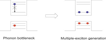
Among third-generation PV technologies, nanostructured materials offer a number of potentially useful properties: (1) The ability to tune the bandgap and the absorption spectrum by changing the size, shape, and surface termination of the nanostructuresReference Pietryga, Schaller, Werder, Stewart, Klimov and Hollingsworth3 could enable the realization of multijunction solar cells made from a single semiconductor material. (2) The ability to synthesize Type II core/shell nanocrystalsReference Kim, Fisher, Eisler and Bawendi4 and nanowiresReference Xiang, Lu, Hu, Yan and Lieber5 (in which the core and the shell have a staggered bandgap alignment) opens the way to achieve exciton dissociation without the need for an applied external field. (3) Efficient multiple-exciton generation (MEG) upon absorption of a single high-energy photon (Figure 1) by semiconductor nanocrystalsReference Schaller and Klimov6–Reference Schaller, Agranovich and Klimov8 or carbon nanotubesReference Wang, Khafizov, Tu, Zheng and Krauss9 could enhance the photocurrent, and thus the photoconversion efficiency, by reducing the fraction of high-energy photons whose excess energy is lost to heat. (4) The existence of a phonon bottleneck that hinders carrier relaxation (Figure 1) could enable hot-carrier transport in nanostructured solar cells, thereby potentially increasing the open-circuit voltage.Reference Nozik10 Although many experimental studiesReference Klimov and McBranch11, Reference Hendry, Koeberg, Wang, Zhang, de Mello Donega, Vanmaekelbergh and Bonn12 have shown that carrier relaxation is very fast in conventional nanostructures (with typical relaxation times of the order of 0.1 ps or lessReference Klimov and McBranch11), specially designed nano-heterostructures were shown to effectively suppress phonon-assisted carrier relaxation.Reference Pandey and Guyot-Sionnest13 (5) Semiconductor quantum dots can also be used to form a partially occupied intermediate band in the bandgap of a host semiconductor.Reference Marti, Antolin, Stanley, Farmer, Lopez, Diaz, Linares and Luque14 This intermediate band can act as an efficient photon up-converter, enabling absorption of sub-bandgap photons and thus overcoming one of the limitations of single-junction solar cells.Reference Shockley and Queisser2
Phonon bottleneck and multiple-exciton generation processes in semiconductor quantum dots. Blue dots represent electrons, red dots holes. If carrier relaxation by phonon emission is inhibited (phonon bottleneck), an exciton can decay by creating an additional electron–hole-pair (multiple-exciton generation).

Nanostructured semiconductors offer additional degrees of freedom over conventional, bulk semiconductors. The size, shape, and spatial distribution of the nanostructures, as well as their surface termination and functionalization with organic ligands, can often be controlled to a high degree of accuracy and reproducibility during synthesis, opening the way to the design of nanomaterials with enhanced solar energy conversion efficiency. However, the ability to explore this large configuration space by synthesis and characterization alone is limited, which makes computational investigations of the electronic and optical properties of nanostructures particularly valuable. Over the last several years, two different computational approaches to the calculation of the properties of nanostructures have been developed: (1) first-principles electronic structure methods, based primarily on density functional theory (DFT), and (2) semi-empirical atomistic methods, such as tight binding or empirical pseudopotential methods. This article reviews recent developments in the implementation and application of atomistic methods to calculate electronic excitations in nanostructures. It also discusses the application of such methods to investigate carrier relaxation, multiple-exciton generation, and charge separation in semiconductor nanostructures.
Computational methods for nanostructures
Calculations of the optical and electronic properties of nanostructured photoconversion materials pose very stringent requirements on computational algorithms and hardware resources. Accurate computations of electronic excitations, and possibly their dynamics, in nanostructures containing hundreds or thousands of atoms are beyond the reach of most electronic-structure and quantum-chemistry codes. During the last decade, however, significant progress has been made in the application of both density-functional methods and semi-empirical methods to nanostructured materials.
DFT has long been the method of choice for first-principles band structure and total-energy calculations of real materials systems. Recent computational and algorithmic developments, coupled with the availability of massively parallel computers, have significantly increased the range of materials and properties that can be investigated using this approach. DFT calculations for systems containing several hundred atoms are now routinely performed, and calculations for 104-atom Si nanostructures have been recently demonstratedReference Chelikowsky, Saad, Chan, Tiago, Zayak and Zhou15 (see the Introduction article in this issue). However, DFT remains essentially a ground-state theory. Indeed, several interesting applications of DFT to determine the ground-state geometry of Si nanoparticles,Reference Zhao, Kim, Du and Zhang16 the vibrational spectrum of carbon nanotubes,Reference Sánchez-Portal, Artacho, Soler, Rubio and Ordejon17 and the bond geometry of CdSe,Reference Puzder, Williamson, Gygi and Galli18 Si,Reference Degoli, Cantele, Luppi, Magri, Ninno, Bisi and Ossicini19 and lead chalcogenides nanocrystalsReference Franceschetti20, Reference Leitsmann and Bechstedt21 have been presented in the literature. However, at the core of the investigation of nanostructures for solar energy conversion is the ability to accurately predict excited-state properties. Two computational approaches to the calculation of electronic excitations of nanostructures are particularly promising: (1) time-dependent density-functional theory (TDDFT) and (2) many-body perturbation theory (MBPT).
In the TDDFT approach, one starts by solving the self-consistent Kohn-Sham equations:

where −∇2 is the kinetic energy (in Rydbergs), and V ext(r), V H(r), and V xc(r) are the external potential, the Hartree potential, and the (approximate) exchange-correlation potential, respectively, which are functions of the spatial coordinate r. The solutions of the Kohn-Sham equations are the single-particle energies εi and wave functions ψi (r). In the linear response approximation to TDDFT, the excitation spectrum is obtained by solving the eigenvalue problemReference Burke, Werschnik and Gross22

where ωi,j = εj − εi is the difference between the Kohn-Sham single-particle energies εj and εi, fi,j = ni – nj is the difference between the occupation numbers of the Kohn-Sham eigenstates i and j, and

where ρ(r) is the DFT charge density. The second term in brackets in Equation 2 produces a shift of the DFT transition energies, ωi,j, yielding the TDDFT excitation energies Ω and oscillator strengths Fi,j. The TDDFT approach has been recently applied to calculate the electronic excited states of SiReference Vasiliev, Ogut and Chelikowsky23–Reference Ramos, Paier, Kresse and Bechstedt25and CdSeReference Troparevsky, Kronik and Chelikowsky26, Reference Lopez del Puerto, Tiago and Chelikowsky27 clusters. Craig et al.Reference Craig, Duncan and Prezhdo28 proposed an extension of TDDFT to study the non-adiabatic dynamics of excited states in molecules and small clusters.
In the MBPT method, the first step is to calculate the quasi-particle energies and wave functions of a nanostructure by solving the Dyson equation
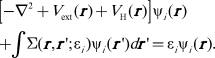
The self-energy ∑(r, r′;ε) is usually calculated in the GW approximation.Reference Hybertsen and Louie29 Excitonic states are then obtained by solving the Bethe-Salpeter equation (BSE):Reference Strinati30

where

and

The eigensolutions Av,c of Equation 5 represent the coefficients of the expansion of the excitonic states in Slater determinants.
Although DFT-based methods are increasingly being applied to realistic nanostructures, they suffer from a few significant drawbacks: (1) The single-particle transition energies and effective masses obtained directly from the Kohn-Sham eigenvalues are notoriously in disagreement with experiment. The calculation of optical and electronic properties of nanostructures thus requires a more advanced approach, such as TDDFT or MBPT. However, (2) TDDFT/MBPT calculations are computationally very demanding and can currently be performed for nanostructures containing only a few dozen atoms, which are usually of limited interest for PV applications. (3) Additionally, neither TDDFT nor MBPT provide a convenient way to describe multiple electron–hole–pairs (multiexcitons) in nanostructures.
These limitations can be overcome using a semi-empirical approach, based on a parameterization of the single-particle Hamiltonian with parameters fitted to bulk experimental properties. Examples include the tight-binding methodReference Niquet, Delerue, Allan and Lannoo31 and the empirical pseudopotential method (EPM).Reference Franceschetti, Fu, Wang and Zunger32 In the EPM approach, one first solves for the single-particle Schrödinger equation

where the total pseudopotential V ps(r) is given by the superposition of screened atomic potentials centered at the positions {Rn} of the atoms in the nanostructure and in the surrounding matrix:
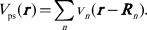
The atomic potentials vn are fitted to bulk experimental transition energies, effective masses, and deformation potentials, as well as bulk first principles wave functions. V pol(r) is the self-energy surface-polarization potential induced by the dielectric mismatch between the nanostructure and the surrounding material. It can be approximated, using classical electrostatics, as  , where W(r,r′) and W bulk(r,r′) are the screened Coulomb potentials of the nanostructure and the bulk material, respectively.Reference Franceschetti and Zunger33
The advantages of using the EPM Equation 8 instead of the Kohn-Sham Equation 1 include the possibility of using a smaller basis set (i.e., a lower energy cutoff in the plane-wave expansion of the wave functions), the fact that the self-consistent cycle can be avoided as the potential in Equation 8 is fixed, and, most importantly, the possibility of directly accessing the band-edge states using the folded-spectrum method,Reference Wang and Zunger34 without the need to calculate lower-energy states as in conventional DFT calculations. The result is that EPM calculations can be easily performed for nanostructures containing tens of thousands of atoms. WangReference Wang35 proposed a slightly different approach, known as the “charge-density patching” method. In this approach, one approximates the total charge density from the superposition of atomic charge densities obtained from a set of DFT calculations. By solving the Poisson equation associated with this charge density, one obtains the potential of the nanostructure. To correct for the DFT bandgap error, a non-local potential fitted to experimental data is added, and the ensuing Schrödinger equation is solved using the folded-spectrum method.Reference Wang and Zunger34
Since the pseudopotential parameters used in Equation 9 are fitted to bulk quasi-particle energies, the eigenvalues of the EPM Equation 8 are good approximations of the solutions of the Dyson Equation 4, without the need to actually solve the GW equations. Carrier-carrier interactions are then included by solving the configuration-interaction (CI) Hamiltonian:Reference Franceschetti, Fu, Wang and Zunger32, Reference Franceschetti and Troparevsky36

Here  (ci) is the creation (annihilation) operator for an electron in the conduction-band state i;
 (dj) is the creation (annihilation) operator for a hole in the valence-band state j; and V, C denote the valence-band and conduction-band manifolds, respectively. The sums in Equation 10 are restricted to the single-particle states included in an “active space” consisting of the first several conduction states above the conduction-band minimum and the first several valence states below the valence-band maximum of the nanostructure. The single-particle energies εi are obtained from the solution of Equation 8, and the Coulomb integrals are given by Equation 6. Since the direct calculation of the screening function ε(r, r′) is computationally very expensive, a phenomenological model is used, described in Reference 32. Unlike the BSE (Equation 5), the CI approach can be used to study multiple excitations, such as biexcitons or charged excitons.
The EPM-CI approach has been successfully applied to study excited properties of semiconductor nanostructures, such as the exciton fine structure,Reference Franceschetti, Fu, Wang and Zunger32 single-exciton and multi-exciton emission and absorption spectra,Reference Franceschetti and Zhang37 and Auger recombination of multiexcitons.Reference Wang, Califano, Zunger and Franceschetti38
Carrier relaxation in semiconductor nanocrystals
Because of quantum confinement, the electronic levels of a nanostructure are separated by relatively large energy gaps, which can significantly exceed typical phonon energies, particularly in the vicinity of the band edges. This observation has led to the suggestion that nanostructures may exhibit a “phonon bottleneck” (Figure 1), whereby phonon-assisted carrier relaxation is inhibited by the lack of phonons with sufficient energy to bridge the gaps between electronic levels.Reference Nozik39 Contrary to this expectation, however, numerous experimental studies have demonstrated fast carrier relaxation for both electrons and holes.Reference Klimov and McBranch11 This surprising result has been attributed to a combination of different mechanisms, such as efficient transfer of excitation energy from electrons to holes,Reference Hendry, Koeberg, Wang, Zhang, de Mello Donega, Vanmaekelbergh and Bonn12 rapid hole relaxation induced by the large hole density of states,Reference Klimov and McBranch11 and coupling of electronic states with surface vibrational modes.Reference Aharoni, Oron, Banin, Rabani and Jortner40 For applications of nanostructures to solar-energy conversion, it would be highly desirable to slow down carrier relaxation as much as possible. Indeed, the existence of a phonon bottleneck could enable extraction of hot carriers from the nanostructures, which, in turn, could significantly increase the open-circuit voltage.Reference Nozik10 Slow carrier relaxation would also enhance the MEG efficiency by lessening competing decay mechanisms for the photo-generated charge carriers.
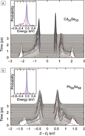
A recent application of non-adiabatic TDDFT to carrier relaxation in nanocrystalsReference Kilina, Kilin and Prezhdo41 (see Figure 2) has revealed relaxation times of the order of a few ps for both the electron and the hole in photo-excited CdSe and PbSe clusters, in qualitative agreement with experimental data. These calculations also have shown a significant acceleration of the carrier relaxation dynamics as the excess energy increases (Figure 2). Additional decay pathways for hot electrons come from fast Auger energy transfer to a photo-excited hole.Reference Wang, Califano, Zunger and Franceschetti38 These seem to preclude the possibility of achieving fast hot-carrier transfer out of the nanocrystals. However, it has been shown that careful engineering of core/shell nanocrystalsReference Pandey and Guyot-Sionnest13 can lead to a substantial reduction of the carrier relaxation rate. This result points to the important role that theory and computation can play in the design of nanostructure architectures with reduced carrier relaxation rates.
Time evolution of the density of states of an electron–hole-pair in (a) a Cd33Se33 cluster and (b) a Pb68Se68 cluster, calculated using non-adiabatic time-dependent density functional theory (from Reference 41). The calculations reveal relaxation times of the order of a few ps for both the electron and the hole in photo-excited CdSe and PbSe clusters, which is in qualitative agreement with experimental data. E, energy; E f, Fermi energy level.

Multiple-exciton generation
Solar cells normally produce a single electron–hole-pair per photon absorbed. The excess photon energy (the energy above the bandgap) is converted to heat and represents a net loss for the photoconversion efficiency. This limitation could be overcome if the excess energy of photons could be used to generate additional electron–hole-pairs (MEG process, Figure 1). While MEG was predicted to be more efficient in nanostructures than in bulk semiconductors,Reference Nozik39 a controversy has recently emerged as to how much, if at all, quantum confinement really enhances MEG. Several experiments have measured the quantum efficiency (QE) of semiconductor nanocrystals (the average number of electron–hole-pairs produced per absorbed photon) as a function of the nanocrystal size and the photon frequency. A QE greater than 1 indicates the presence of MEG. However, the QE depends not only on the MEG rate, but also on the rate of competing decay processes, such as phonon-assisted carrier relaxation. Thus, in order to achieve a better understanding of the effects of quantum confinement on MEG, it would be useful to investigate the size dependence of the MEG rate. This quantity is difficult to measure experimentally but has recently become accessible to accurate semi-empirical calculations.Reference Allan and Delerue42–Reference Rabani and Baer43
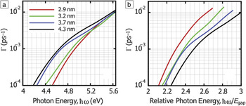
Lin et al.Reference Lin, Franceschetti and Lusk44 have reported semi-empirical pseudopotential calculations of the size and energy dependence of the exciton-to-biexciton decay rate of CdSe nanocrystals of realistic size (up to 4.3 nm), as a function of photon energy and nanocrystal diameter. The calculations were performed using Fermi’s golden rule, where the Coulomb matrix elements were calculated directly from atomistic pseudopotential wave functions. The MEG rate Γ of CdSe nanocrystals was found to increase rapidly with photon energy. At fixed absolute photon energy (Figure 3a), Γ increases as the diameter of the nanocrystal increases. However, at fixed relative photon energy (Figure 3b), Γ displays the opposite trend (i.e., the MEG process becomes faster as the diameter decreases). It has been arguedReference Beard, Midgett, Hanna, Luther, Hughes and Nozik45 that the MEG efficiency is proportional to the slope of the QE versus the relative photon energy ħω/E gap (where ħ is the reduced Planck’s constant, ω is the angular frequency, and E gap is the bandgap energy). This suggests that the relevant quantity to gauge the MEG efficiency is Γ(ħω/E gap), which increases with quantum confinement (see Figure 3b).
Multiple-exciton generation (MEG) decay rate of photo-generated electron–hole-pairs in CdSe nanocrystals of different diameters, as a function of (a) the absolute photon energy and (b) the relative photon energy. At fixed absolute photon energy (a), the MEG rate increases as the size increases, whereas the opposite is true when the relative photon energy is kept fixed (b).Reference Lin, Franceschetti and Lusk44 ħ, reduced Planck’s constant; ω, angular frequency; E gap, bandgap energy; Γ, multiple-exciton generation rate.

Exciton dissociation and charge separation in nanostructures
One of the most challenging problems facing the design of nanostructured photovoltaics is the extraction of photo-generated carriers before they recombine. In conventional p-n junction solar cells, carrier separation is usually achieved by the electrostatic field induced by doping. In nanostructured solar cells, however, photo-generated excitons may be strongly localized in the nanostructures, because of quantum confinement effects and enhanced electron-hole Coulomb attraction. Furthermore, multiexcitons produced by MEG have a very short non-radiative lifetime, due to efficient Auger recombination of electron–hole-pairs,Reference Wang, Califano, Zunger and Franceschetti38, Reference Klimov, Mikhailovsky, McBranch, Leatherdale and Bawendi46 which limits the amount of time available for carrier extraction. Thus, novel approaches to exciton dissociation and charge separation may be required in nanostructured solar cells.
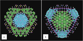
Type II nanoheterostructures provide a convenient way of separating the electron and hole wave functions by enforcing a staggered bandgap alignment, whereby the hole and the electron are localized in different regions of the nanostructure. An example of such nanoheterostructures is a GaN/GaP “coaxial” nanowire. Empirical pseudopotential calculationsReference Zhang, Wang and Mascarenhas47 have shown that the electron is confined in the GaN “core,” while the hole is confined in the GaP “shell” (Figure 4a). Conversely, in a GaP/GaN nanowire, the electron is confined in the GaN shell, while the hole is confined in the GaP core (Figure 4b).
Electron (blue) and hole (green) wave function amplitudes of (a) GaN/GaP and (b) GaP/GaN “coaxial” nanowires (from Reference 47). For (a), the electron is confined to the GaN core, while the hole is confined to the GaP shell. For (b), the hole is confined to the GaP core, and the electron is confined to the GaN shell. These results demonstrate a convenient way of separating the electron and hole wave functions by enforcing a staggered bandgap alignment in a nanowire heterostructure.

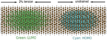
Wu et al.Reference Wu, Neaton and Grossman48 proposed a different design of Type II nanowires. Based on first-principles DFT calculations, they suggested that a Si nanowire, where one segment is subject to tensile strain, would display a Type II band alignment, with the electron localized on the strained segment and the hole on the unstrained segment (Figure 5). This leads to a “longitudinal” electron-hole separation, which could facilitate charge collection in a nanowire solar cell device.Reference Wu, Neaton and Grossman48
The highest occupied molecular orbital (HOMO) and lowest unoccupied molecular orbital (LUMO) wave function amplitudes of a locally strained Si nanowire (from Reference 48). (a) The electron is localized in the strained segment, and (b) the hole is localized in the unstrained segment. This behavior leads to “longitudinal” electron-hole separation and could facilitate charge collection in a nanowire solar device.

Conclusions
Future applications of nanostructured materials to photoconversion technologies would greatly benefit from the development of computational approaches able to identify the nanostructure features that are more relevant to the photoconversion process and to screen different materials combinations for those that can enhance photoconversion efficiency. In recent years, the convergence of new computational methods, numerical algorithms, and massively parallel hardware architectures has made possible, for the first time, accurate atomistic calculations of electronic excitations in semiconductor nanostructures, including their time evolution and dynamics. However, significant challenges remain. First-principles methods, such as time-dependent density functional theory and many-body perturbation theory, are computationally very demanding and cannot yet address multi-particle excitations. Semi-empirical methods, such as tight binding or empirical pseudopotential method, have difficulty describing the effects of surface passivation and/or functionalization of nanostructures. Over the next few years, progress in this area will most likely come from cross fertilization and integration of ab initio and semi-empirical methods. A combined approach, which builds on the strengths of each method, will open the way to the design of nanostructures with enhanced photo-conversion efficiency.