Introduction
Architected materials are a class of materials that are rationally designed or naturally inspired, three-dimensional (3D), multiscale, and often incorporating multiple materials. They have the potential to provide breakthrough performance for a variety of applications if they can be realized at large enough overall size scales, with adequate throughput, and from the appropriate constituent materials. For the most part, remarkable properties of these materials have been demonstrated through cumbersome fabrication processes or with small samples in academic settings. Recently, with acceleration in the development of additive manufacturing (AM) techniques, hierarchical, 3D architected materials have become more accessible.
Historically, architected materials have been fabricated by machining, folding, brazing, joining, and other more conventional processes that have either not been able to achieve the necessary feature resolution or the 3D complexity. This, combined with the typically slow and sometimes costly nature of these processes, has limited the adoption of architected materials. AM, more colloquially referred to as 3D printing, adds material and builds up structure in a layer-by-layer fashion as opposed to material removal methods. As a result, its strength is geometric complexity. This makes printing methods the ideal class of manufacturing techniques for realizing architected materials.
Since their properties arise from geometry and scale as opposed to chemical composition alone, architected materials require accurate and precise physical replication of complex rational designs with minimal defects. Faithful reproduction demands feature sizes ranging from the nano- to the macroscale, complex curvatures, unique material combinations and composites, as well as reproducibility.
Fundamental challenges in fabrication of architected materials
The concept of architected materials has existed for decades and has been most commonly applied in the aerospace industry. Typically, this has been in the form of honeycomb sandwich panel structures, due to their relative ease of fabrication and assembly, and somewhat beneficial performance. These structures have been popular due to their light weight and high bending stiffness; they have also been used with composite materials in thermal protection systems. While relatively easy to fabricate, they are far from optimal geometries for their intended use. In some historical examples, these materials were actually quite costly, but ultimately required, such as in NASA’s Apollo space capsule heat shield where “the advantage of having the fail-safe features of a monolithic heat shield embedded in a honeycomb matrix overrode the disadvantages of extended manufacturing schedules and more costly inspection procedures.”Reference Pavlosky and St. Leger1 In this case, the thermal protection system was not just a honeycomb matrix, but also a multimaterial structure where the fiberglass matrix cells were manually infilled with an epoxy resin material.
To move beyond simple honeycomb sandwich panels and realize the full benefit of architected materials, there are a host of fabrication challenges that must be overcome. These include:
• Complex 3D geometries—Advanced design methods and new functionalities of architected materials are rapidly being explored. These necessitate a complex underlying structure in order to perform as designed. Two-dimensional (2D) structures manually assembled into 3D geometries is not a viable approach to achieve the needed architectures because the desired 3D geometry can either not be achieved or the assembly process is simply too slow and costly.
• Multiscale structure—In the last five years, it has become clear that hierarchical architectures with features ranging from the nanoscale to the macroscale are of tremendous benefit. One key example is the nanoscale size effect, where enhanced strength and ductile-like properties can be achieved at remarkably low densities and in constituent materials that are normally quite brittle.Reference Meza, Das and Greer2–Reference Zheng, Smith, Jackson, Moran, Cui, Chen, Ye, Fang, Rodriguez, Weisgraber and Spadaccini5 Feature sizes in the tens of nanometers or smaller are required to realize these properties; however, the ability to fabricate at these size scales in overall component or material billet sizes in the centimeter to meter range is elusive.
• Multimaterial structure—Many remarkable properties can be achieved through the design and manufacture of architected materials with multiple material constituents, such as negative thermal expansionReference Hopkins, Lange and Spadaccini6,Reference Wang, Jackson, Ge, Hopkins, Spadaccini and Fang7 or bioinspired high toughness architectures.Reference Munch, Launey, Alsem, Saiz, Tomsia and Ritchie8,Reference Weaver, Milliron, Miserez, Evans-Lutterodt, Herrera, Gallana, Mershon, Swanson, Zavattieri, DiMasi and Kisailus9 The ability to arrange and join multiple materials in 3D space is a critical challenge.
• Materials diversity—As architected materials advance rapidly, functionalities beyond static structural and mechanical properties are becoming accessible. This ranges from energy storageReference Yao, Chandrasekaran, Zhang, Xiao, Qian, Zhu, Duoss, Spadaccini, Worsley and Li10,Reference Xia, Afshar, Yang, Portela, Kochmann, Di Leo and Greer11 to shape- and property-changing materials and structures.Reference Coulais, Teomy, De Reus, Shokef and Van Hecke12–Reference Jackson, Messner, Dudukovic, Smith, Bekker, Moran, Golobic, Pascall, Duoss, Loh and Spadaccini14 The constituent materials needed to provide these functionalities can be challenging for fabrication. Feedstocks for AM processes can be loaded with particle fillers that consist of nanomaterials that could be difficult to deal with, and often require significant post-processing.
• Manufacturing throughput—For architected materials to be adopted for widespread use, manufacturing of these exquisite underlying structures must be done at reasonable speed and cost. While current technologies can realize some of these remarkably detailed architectures, industrial-scale throughput is generally not available. This represents a significant challenge and opportunity for manufacturing of architected materials.
Advanced and evolving AM techniques can be used to address many of these challenges. However, these methods are still being developed and, in many cases, not widely available. They can generally be divided into two primary classes: light-based techniques and extrusion-based methods.
Light-based methods for fabrication of architected materials
Using light to create 3D structures has been a core concept in AM since C. Hull patented his stereolithography process in 1986.Reference Hull15 Since its inception, stereolithography has been capable of creating complex 3D structures such as those found in architected materials by rastering a laser over a photopolymerizable liquid. Due to the flexibility of light-based AM processes, they are well suited to address some of the challenges previously mentioned.
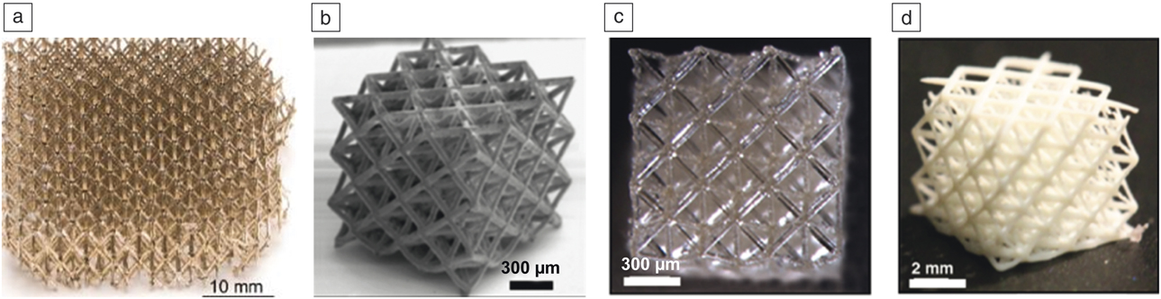
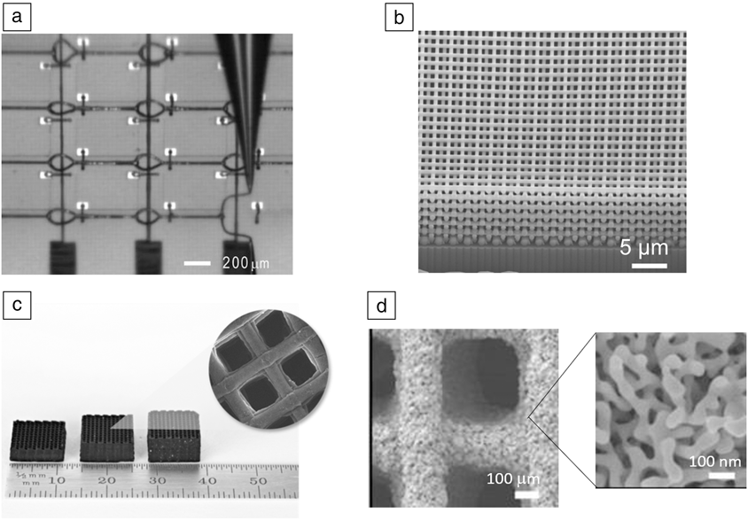
An example of a novel light-based process that addresses the need of high-throughput manufacturing of architected materials is self-propagating photopolymer waveguide prototyping. This process uses a static mask and collimated ultraviolet (UV) light to create a 3D array of self-propagating waveguides. As light passes through the mask and enters a photopolymer liquid bath, solid material forms along the path of the light. By varying the angle of the incident light and the openings in the mask, a set of interconnected beams forming a cellular lattice structure can be created in seconds to minutes. Subsequent post-processing, such as electroless plating of nickel, can add new materials and features to the architecture. By etching the original polymer away, hollow tubes with thin walls are formed, creating one of the first examples of a high mechanical performance, high manufacturing throughput, architected material.Reference Schaedler, Jacobsen, Torrents, Sorensen, Lian, Greer, Valdevit and Carter16 Figure 1a shows an example structure from this process. The primary limitation of this waveguiding method is geometric flexibility; only certain angles are attainable, and architectures are limited to primarily beam-based structures.
(a) Hollow tube metallic microlattice created with self-propagating photopolymer waveguide prototyping,Reference Schaedler, Jacobsen, Torrents, Sorensen, Lian, Greer, Valdevit and Carter16 (b) polymeric microarchitected material fabricated using projection micro-stereolithography (PμSL),Reference Zheng, Lee, Weisgraber, Shusteff, DeOtte, Duoss, Kuntz, Biener, Ge, Jackson, Kucheyev, Fang and Spadaccini18 (c) hollow tube alumina architecture generated with PμSL and atomic layer deposition (ALD) coating,Reference Zheng, Lee, Weisgraber, Shusteff, DeOtte, Duoss, Kuntz, Biener, Ge, Jackson, Kucheyev, Fang and Spadaccini18 and (d) solid ceramic architected material derived from PμSL with alumina nanoparticles in the liquid monomer suspension followed by a sintering step.Reference Zheng, Lee, Weisgraber, Shusteff, DeOtte, Duoss, Kuntz, Biener, Ge, Jackson, Kucheyev, Fang and Spadaccini18

Projection micro-stereolithography (PμSL) is a version of stereolithography that uses UV light-emitting diode (LED) arrays to create 2D projections from a spatial light modulator (SLM) onto a photosensitive liquid resin. Specialized optics reduce the image size so that microscale features in the x-y plane can be achieved. Resolution on the z-axis is set by the fluid properties of the liquid and can be microscale as well. In PμSL, rather than rastering a point as is done in traditional stereolithography, an entire 2D layer is created at once via the projection, which fundamentally changes the process from a one-dimensional (1D) operation to a 2D area-based process and increases throughput dramatically as a result.Reference Zheng, DeOtte, Alonso, Farquar, Weisgraber, Gemberling, Lee, Fang and Spadaccini17
While PμSL has been a remarkable process for creating architected materials such as those shown in Figure 1b, the overall sample sizes can be quite small, and the range of materials limited.Reference Zheng, Lee, Weisgraber, Shusteff, DeOtte, Duoss, Kuntz, Biener, Ge, Jackson, Kucheyev, Fang and Spadaccini18 As with the waveguiding technique, post-processing can expand the available materials palette for light-based polymeric AM processes. For example, Figure 1c shows an architected material made using a PμSL polymeric template, which was coated with a thin film of alumina via atomic layer deposition (ALD). Subsequent removal of the polymer through etching or thermal decomposition leaves ceramic hollow tubes with nanoscale wall thickness.Reference Zheng, Lee, Weisgraber, Shusteff, DeOtte, Duoss, Kuntz, Biener, Ge, Jackson, Kucheyev, Fang and Spadaccini18 Similarly, in Figure 1d, PμSL was used with alumina nano- and microparticles suspended in a liquid resin resulting in a composite architected material. Thermal post-processing was used to remove the polymer matrix while sintering the ceramic particles to near 95% dense alumina.Reference Zheng, Lee, Weisgraber, Shusteff, DeOtte, Duoss, Kuntz, Biener, Ge, Jackson, Kucheyev, Fang and Spadaccini18
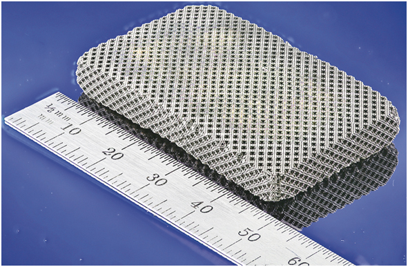
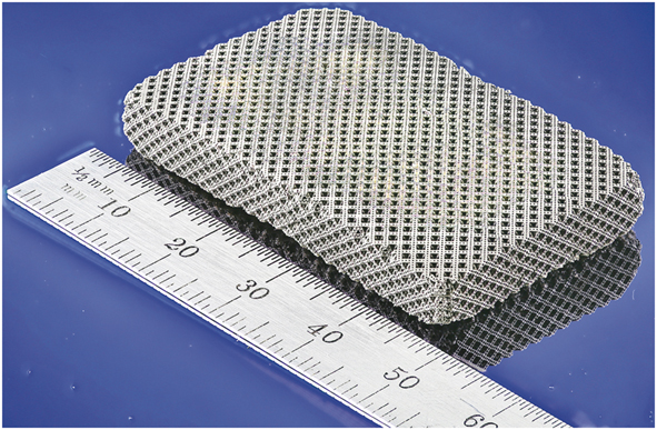
Attempts have been made to scale up the PμSL process for significantly larger overall part sizes while maintaining microscale features. A large-area version of this was developed by scanning the projected light over the surface of the liquid photoresin using scanning galvanometric mirrors. Taking advantage of the dynamic SLM-based projection system, the scanning image can be changed based on the x-y location of the light. Because the light is scanned rather than expanded to cover more area, the resolution of the system is not compromised, but there is an inherent tradeoff with throughput as the entire build area is not illuminated at one time. However, this adaptation allows for fabrication of near arbitrary 3D microscale features over tens of centimeters length scales. Combined with some of the post-processing methods previously described, such as thin-film coatings, complex 3D structures with overall sizes of centimeters can be created with microscale features and wall thicknesses in the tens of nanometers range, as shown in Figure 2.Reference Zheng, Smith, Jackson, Moran, Cui, Chen, Ye, Fang, Rodriguez, Weisgraber and Spadaccini5
Hollow tube, hierarchical architected material fabricated using large-area scanning projection micro-stereolithography (PμSL) followed by electroless nickel plating and etching of the polymer core.Reference Zheng, Smith, Jackson, Moran, Cui, Chen, Ye, Fang, Rodriguez, Weisgraber and Spadaccini5
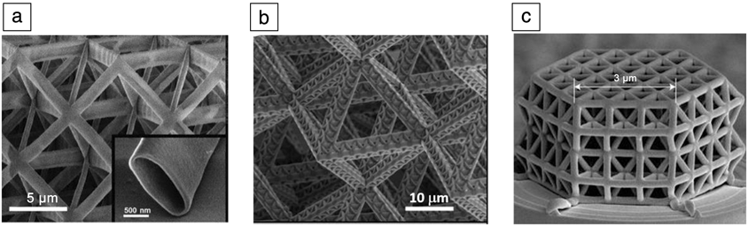
Two-photon polymerization (2PP) is an AM process capable of producing features in the 100–200-nm size range by utilizing two-photon absorption. At the focal point of an ultrashort laser pulse that is directed into a photosensitive resin, the two-photon absorption process results in polymerization. The polymerization threshold of the resin is tuned to be nonlinear, resulting in features that are below the diffraction limit. The solidified volume element, often referred to as a voxel, moves throughout the resin as the laser is rastered to draw out submicron features in 3D.Reference Maruo, Nakamura and Kawata19,Reference Malinauskas, Žukauskas, Bičkauskaitė, Gadonas and Juodkazis20 This technique has been widely used to create architected materials with nanoscale features. Figure 3 shows some of the exquisite architectures that have been generated using 2PP. At these feature sizes and with post-processing methods such as thin-film coatings and pyrolysis, some of the most impressive mechanical properties of any architectures have been achieved.
Exquisite architectures fabricated with two-photon polymerization; (a) hollow tube ceramics obtained by atomic layer deposition (ALD) coating and polymer etching,Reference Meza, Das and Greer2 (b) hierarchical polymer architectures,Reference Meza, Zelhofer, Clarke, Mateos, Kochmann and Greer3 and (c) glassy carbon nanolattices obtained by pyrolysis of the polymer.Reference Bauer, Schroer, Schwaiger and Kraft4

The primary drawback of 2PP in the context of architected materials is throughput. Complexity and resolution are its strengths, but due to the 1D nature of serial scanning, it is a slow process. For example, the time required to fabricate a solid, nonporous structure 150 μm × 150 μm × 1000 μm could be in excess of 2 h. There are some research efforts throughout the community endeavoring to scale up the process for radically improved throughput. Exciting new developments and breakthroughs along these lines are expected via parallelization of the 2PP process.
A completely new class of light-based AM methods has recently been introduced: volumetric additive manufacture (VAM). Development of these techniques is nascent, but incredibly promising. It is based upon the concept of moving AM processes from the assembly of 1D elements (voxels) or 2D areas (projections) to fully 3D operations.
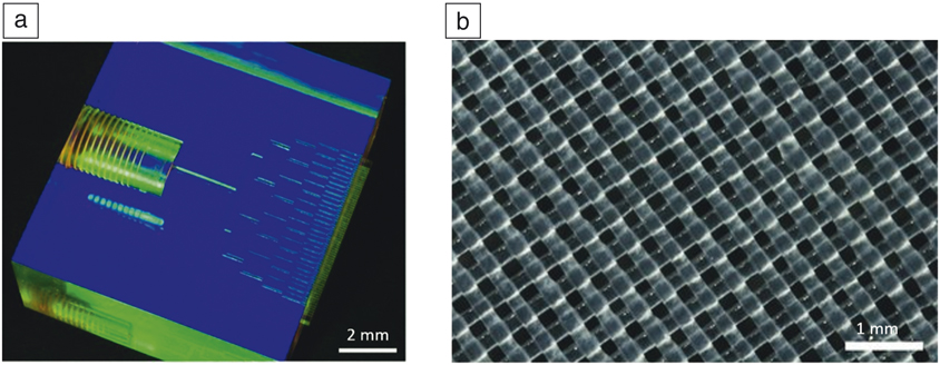
The first instantiation of this concept was achieved by intersecting multiple patterned lasers in space to form a higher intensity light field in 3D. This pattern, similar to a hologram but actually only the superposition of light at the intersections, is projected into a vat of photosensitive resin. This results in more rapid curing of resin material at the higher intensity locations, forming the entire 3D structure defined by the intersections in a single exposure of laser illumination. Typically, simple components can be formed in ∼10 s as an entire volume.Reference Shusteff, Browar, Kelly, Henriksson, Weisgraber, Panas, Fang and Spadaccini21 Figure 4a–b shows a schematic and example part, respectively. While this is clearly an exciting concept due to the potential throughput, the geometric complexity is limited.
Volumetric additive manufacturing; (a) schematic of lasers intersecting in space to form a 3D light field,Reference Shusteff, Browar, Kelly, Henriksson, Weisgraber, Panas, Fang and Spadaccini21 (b) a component fabricated volumetrically in ∼10 s,Reference Shusteff, Browar, Kelly, Henriksson, Weisgraber, Panas, Fang and Spadaccini21 (c) schematic of the setup for computed axial lithography.Reference Kelly, Bhattacharya, Heidari, Shusteff, Spadaccini and Taylor22 DLP is digital light processor. (d) Schematic of intensity weighted images to be projected at different angles into a vat of photoresin to form Rodin’s “The Thinker” statue,Reference Kelly, Bhattacharya, Heidari, Shusteff, Spadaccini and Taylor22 and (e) “The Thinker” after fabrication using computed axial lithography (CAL) in about 50 s, still in the vat of photoresin.Reference Kelly, Bhattacharya, Heidari, Shusteff, Spadaccini and Taylor22

Subsequently, a more sophisticated VAM technique was developed. This method relies upon the use of tomographic reconstruction algorithms. These algorithms are applied to a 3D CAD model to generate intensity weighted images at various angles through the 3D model. The images are then projected as a continuous movie into a rotating vat of photosensitive resin and timed accordingly. By dosing the 3D space with light as the vat rotates, the entire structure forms, without layers or voxels, in a matter of seconds to minutes and can have near arbitrary geometry.Reference Kelly, Bhattacharya, Heidari, Shusteff, Spadaccini and Taylor22 This version of VAM has been aptly named computed axial lithography (CAL). Figure 4c–e shows process schematics and an example of a fabricated component still in its liquid vat. While seemingly quite powerful for rapidly forming complex structures, only simple architectures have been demonstrated to date. The potential for CAL is enormous, however, and work is ongoing to understand the limits of this exciting new process.
Materials advancements for light-based AM processes are critical to moving architected materials forward. A key limitation to these methods is the fact that the initial feedstock material must be photosensitive and highly tuned to the fabrication process. One technique to access other material classes, such metals and ceramics, is to use the initial polymer architecture as a template for a subsequent coating process such as ALD or electroless plating, as shown in Figures 1 and 2. It was also shown in Figure 1d that suspensions of nanoparticles in the feedstock resins could be sintered to form solid ceramics.
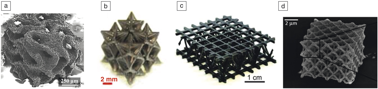
Other interesting fillers with more functional properties have recently been demonstrated. For example, graphene oxide platelets can be dispersed into photosensitive resins and formed into a green body via the PμSL process. After drying and pyrolysis, this can be converted to graphene aerogel where the fabricated structure consists of platelets of graphene at the nanoscale. This represents a hierarchical architected material where the high surface area, electrically conductive, yet stochastic nanomaterial is the primary constituent making up the higher length scale architecture such as the graphene aerogel gyroid shown in Figure 5a.Reference Hensleigh, Cui, Oakdale, Ye, Campbell, Duoss, Spadaccini, Zheng and Worsley23 Fillers have also been used in initial examples of multimaterial architectures made with PμSL. Figure 5b shows a negative thermal expansion architected material, where one component of the architecture is loaded with copper particles and the other is pure polymer. This was achieved by dispensing different materials into the fabrication area at different times during the build.Reference Wang, Jackson, Ge, Hopkins, Spadaccini and Fang7
(a) A gyroid architecture made of a graphene aerogel fabricated with projection micro-stereolithography (PμSL),Reference Hensleigh, Cui, Oakdale, Ye, Campbell, Duoss, Spadaccini, Zheng and Worsley23 (b) a multimaterial negative thermal expansion architected material fabricated with PμSL,Reference Wang, Jackson, Ge, Hopkins, Spadaccini and Fang7 (c) a SiOC lattice made from a preceramic monomer in a stereolithography system,Reference Eckel, Zhou, Martin, Jacobsen, Carter and Schaedler24 and (d) a metallic nanolattice generated from nickel acrylate in two-photon lithography.Reference Vyatskikh, Delalande, Kudo, Zhang, Portela and Greer25
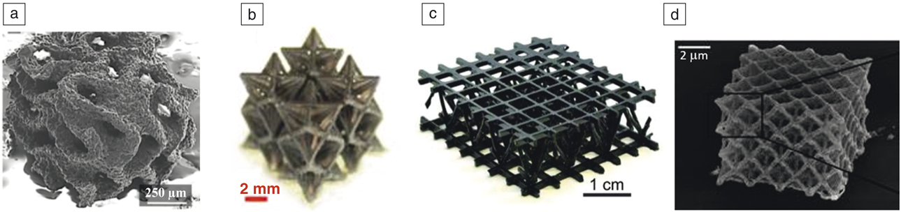
More recent developments have moved away from particle-based fillers and external coatings to preceramic monomers and chemistries with integrated metallics such as nickel acrylate. While thermal post-processing is still required, the advantages of these feedstocks include more chemically pure final structures, potentially reduced defects and porosity, and well-behaved isotropic shrinkage. Figure 5c shows work by Eckel at al. who demonstrated the use of a preceramic monomer in a stereolithography process. After pyrolysis, the siloxane-based material converted to SiOC with only about 30% linear shrinkage and excellent overall shape retention.Reference Eckel, Zhou, Martin, Jacobsen, Carter and Schaedler24 Similarly, Greer and colleagues used a nickel acrylate in the 2PP process, followed by a two-step pyrolysis, to form the metallic nanolattices shown in Figure 5d.Reference Vyatskikh, Delalande, Kudo, Zhang, Portela and Greer25
Extrusion-based methods for fabrication of architected materials
Any discussion of AM and processing for architected materials would be incomplete without mention of extrusion-based printing methods. These techniques represent some of the first methods used to create architected materials. The most common 3D printing approach used worldwide is extrusion of thermoplastic materials through heated nozzles, known as fused deposition modeling (FDM). This technique has been used for larger-scale models of architectures, or even for some actual demonstrations at higher length scales.
More common for high-performance, hierarchical, architected materials is the direct ink write (DIW) method, which primarily functions through manipulating the rheology of the printed material, or “ink,” such that it behaves as a shear thinning paste. Simply put, in the presence of shear, as would be the case in a nozzle with force applied to the material, it will flow. In the absence of that shear, as the material exits the nozzle, it will gel and hold the approximate cross-sectional shape of the nozzle from which it has been extruded. In order to create an ink material with these properties, careful attention is paid to the complex rheology, including the shear storage and loss moduli, G′ and G″, respectively. In a low shear environment, a printable ink should be dominated by the storage modulus, which represents solid-like behavior. As shear is increased, the loss modulus begins to dominate and represents liquid-like behavior of the viscoelastic material. The change-over from one to the other is tuned such that the ink flows and gels at the proper shear rates for printing.Reference Lewis26,Reference Lewis27 This tuning can be affected by the addition of particles, surfactants, viscosifiers, and other chemical additives.
While DIW fabricated structures tend to be limited to filamentary-based architectures due to the extrusion process, their primary advantage in the context of architected materials is the diversity of constituent materials that can be made to work with the process and the range of accessible size scales. Because particles can help to tune the rheology, DIW is particularly amenable to inks that are highly filled with particles. For example, metallicReference Ahn, Duoss, Motala, Guo, Park, Xiong, Yoon, Nuzzo, Rogers and Lewis28 and ceramicReference Lewis26,Reference Duoss, Twardowski and Lewis29 architectures can be readily achieved by printing a filled ink and subsequent thermal post-processing. An example is shown in Figure 6a.
(a) Direct ink write (DIW) of a silver ink forming electrical interconnects,Reference Ahn, Duoss, Motala, Guo, Park, Xiong, Yoon, Nuzzo, Rogers and Lewis28 (b) a DIW titania lattice with submicron filaments made from a particle-free sol-gel ink,Reference Duoss, Twardowski and Lewis29 (c) DIW printed graphene aerogel with high specific surface area and good electrical conductivity,Reference Zhu, Han, Duoss, Golobic, Kuntz, Spadaccini and Worsley31 and (d) DIW generated nanoporous gold obtained via dealloying of a gold-silver alloy after printing.Reference Zhu, Qi, Beck, Luneau, Lattimer, Chen, Worsley, Ye, Duoss, Spadaccini, Friend and Biener30

Microscale resolution can be achieved with particle-based inks provided that the particles themselves are small enough to not clog the nozzle (particles are typically 1–2 orders of magnitude smaller than the nozzle size) and are well dispersed throughout the ink. Single-digit micrometer and even submicron features are attainable if the ink is particle-free, such as titania sol-gel ink, which makes up the architecture shown in Figure 6b.Reference Duoss, Twardowski and Lewis29
Functional and hierarchical architectures are also possible with this method. For example,Reference Zhu, Han, Duoss, Golobic, Kuntz, Spadaccini and Worsley31 a printable ink filled with graphene oxide platelets was created and extruded into a liquid matrix to prevent stacking of the graphene oxide sheets. This was followed by supercritical drying and a pyrolysis step to convert the material into a graphene aerogel. This architected material consists of an ordered structure at the microscale and stochastic graphene at the nanoscale. It is remarkable due to its high surface area, approaching 1000 m2/g, and good electrical conductivity, making it a useful energy storage material for devices such as supercapacitors. While the nanomaterial gives the overall architecture its functional characteristics, the ordered architecture can be designed for specific mechanical properties or to reduce pressure drop of a fluid flowing through the structure.Reference Zhu, Han, Duoss, Golobic, Kuntz, Spadaccini and Worsley31 Similarly, a hierarchical nanoporous gold material was DIW printed by first extruding an alloy of gold and silver and then subsequently dealloying the material to remove the silver component.Reference Zhu, Qi, Beck, Luneau, Lattimer, Chen, Worsley, Ye, Duoss, Spadaccini, Friend and Biener30 Figure 6c–d shows these hierarchical architectures, respectively.
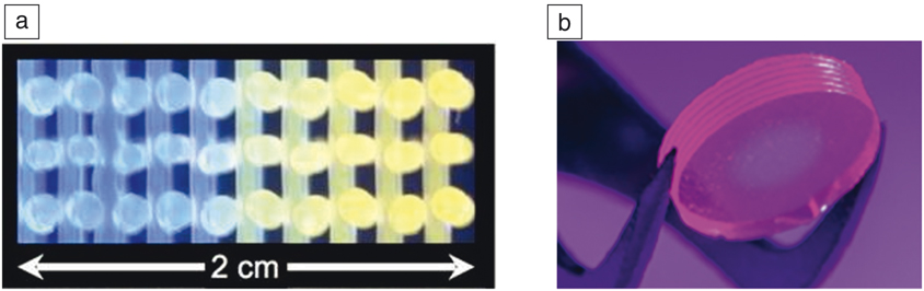
DIW is also amenable to multimaterial printing. The obvious method to achieve this is to use multiple nozzles, each with a different material, to create a multimaterial architecture. While this has certainly been done, more exciting is the recently proven ability to mix materials on the fly in the nozzle during a printing operation to control material composition as well as architecture. This can be done through static mixing with swirl-inducing structures built into the printhead itself to wrap two flows around each other, increasing interfacial area between high-viscosity materials.Reference Ober, Foresti and Lewis32 The drawback of static mixing is the time required to change material composition. In order to vary material composition quickly with high-viscosity inks, mixing must be performed in small volumes and with an active mixing element such as a rotating paddle or screw.Reference Ober, Foresti and Lewis32–Reference Golobic, Durban, Fisher, Grapes, Ortega, Spadaccini, Duoss, Gash and Sullivan35 Figure 7 shows varying composition structures made using DIW.
Mixing on the fly during direct ink write (DIW) printing to create graded materials. (a) Cross section of a printed silicone lattice with a gradient in fluorescent dye,Reference Ober, Foresti and Lewis32 and (b) a DIW printed silica optic with a gradient in gold nanoparticles as a demonstration of the potential for a gradient index optic.Reference Nguyen, Meyers, Yee, Dudukovic, Destino, Zhu, Duoss, Baumann, Suratwala, Smay and Dylla-Spears33

The material diversity of DIW is impressive; however, it is a 1D operation, similar to 2PP, where a single point is moved serially around a build plane. This fundamentally limits the throughput of DIW. However, there are approaches being explored to increase speed while maintaining resolution. While the ink itself can be tuned to flow faster out of the nozzle, there are limits to what can be achieved through these means, as maintaining the shear thinning behavior of the material is paramount. Another concept is to parallelize the process through a multinozzle array, as shown in Figure 8.Reference Hansen, Saksena, Kolesky, Vericella, Kranz, Muldowney, Christensen and Lewis36 This would obviously increase the throughput of the printing methods, but at the expense of geometric flexibility. The overall architecture of the structure would be set by the spacing and geometry of the nozzle array.
Direct ink write (DIW) scale-up. (a) Multinozzle array formed from a bifurcating network of microfluidic channels,Reference Hansen, Saksena, Kolesky, Vericella, Kranz, Muldowney, Christensen and Lewis36 and (b) a wood-pile lattice structure created with the multinozzle array.Reference Hansen, Saksena, Kolesky, Vericella, Kranz, Muldowney, Christensen and Lewis36

Summary and future directions
AM processes are advancing rapidly with new methods and materials impacting our ability to realize architected materials in a meaningful way. Nanoscale resolution is now readily available, 3D complexity is at our fingertips, and the palette of available materials expands with every publication. However, significant challenges remain in multimaterial and multiscale AM, while overall manufacturing throughput still remains an enormous gap to realizing architected materials in industrial applications.
While light-based and extrusion-based printing methods provide excellent opportunities to address these challenges, there may be others that will contribute as well. AM processes such as laser- or electron-beam powder-bed fusion, laser direct deposition, wire-based methods, polyjet printing, and binder printing all may play a role. There may be new processes yet to be invented that we have not even conceived of, nor should we neglect the possible contributions of more traditional fabrication methods such as semiconductor processing and micromachining.
Expanding the diversity of material constituents available for architected materials is going to continue to drive advances in AM. The ability to handle multiple materials and join them in a structure, or blend materials creating designed gradients within architectures would be a powerful tool. Biomaterials are an enormous opportunity for architected materials as well. While bioprinting is an extremely active area of research, adding the element of architecture, or scaffolds as they are called in biology, and tailored design of properties would enhance cell growth for a variety of applications. As AM and architected materials move more into the realm of functional materials, unique combinations of properties may result from the integration of multiple disparate physics such as structural mechanics with electromagnetics.
The possibilities and opportunities for architected materials are extraordinary provided the manufacturing and processing technologies advance with corresponding speed and agility. Moving forward, new and improved AM processes will be core tools for the advancement and realization of architected materials.
Acknowledgments
This work was performed under the auspices of the US Department of Energy by Lawrence Livermore National Laboratory under Contract No. DE-AC52–07NA27344. LLNL-JRNL-787998.

Christopher M. Spadaccini is currently the director of the Additive Manufacturing Initiative as well as the leader of the Center for Engineered Materials and Manufacturing, both at Lawrence Livermore National Laboratory. He is also an adjunct faculty member at the University of California, Davis, in the Department of Chemical Engineering. He received his BS, MS, and PhD degrees from the Department of Aeronautics and Astronautics at the Massachusetts Institute of Technology in 1997, 1999, and 2004, respectively. He has more than 60 journal publications, four book chapters, and approximately 60 invited presentations and 35 patents awarded or pending. His research interests include new additive and advanced manufacturing processes with a focus on micro- and nanoscale features and mixed materials as well as architected materials. Spadaccini can be reached by email at spadaccini2@llnl.gov.