Introduction
Organic–inorganic halide perovskite semiconductors of the chemical formula ABX3 have been the focus of the photovoltaic community for over half a decade for their remarkable optoelectronic properties, most notably the ability to produce a large photopotential even with substantial structural defects [Reference Snaith1, Reference Green, Ho-Baillie and Snaith2, Reference Manser, Christians and Kamat3]. The power conversion efficiency (PCE) of perovskite solar cells is now on par with that of commercial photovoltaic modules [Reference Kaltenbrunner, Adam, Glowacki, Drack, Schwodiauer, Leonat, Apaydin, Groiss, Scharber, White, Sariciftci and Bauer4]. Along with such high efficiencies, perovskites boast a high and tunable band gap, high light absorption coefficient, long diffusion lengths, slow recombination kinetics, high carrier mobility, and importantly the ability to be processed from solution, thereby allowing low-cost, high-throughput fabrication at low temperature and on a variety of substrate types. The rich variety of compositions and the multitude of ways in which they can be investigated have sustained an ever-increasing level of attention in perovskites and related materials [Reference Snaith1, Reference Green, Ho-Baillie and Snaith2, Reference Manser, Christians and Kamat3, Reference Kaltenbrunner, Adam, Glowacki, Drack, Schwodiauer, Leonat, Apaydin, Groiss, Scharber, White, Sariciftci and Bauer4, Reference Manser, Saidaminov, Christians, Bakr and Kamat5].
Perovskites typically adopt an ABX3 formulation, where A is the methylammonium (CH3NH3) or formamidinium [HC(NH2)2] cation, B is commonly lead (Pb), and X is a halide (Cl, Br, I). This layer is typically sandwiched between an electron transport layer (ETL) and a hole transport layer (HTL). A top contact of a transparent conducting oxide, typically fluorine-doped tin oxide (FTO), and a bottom (or back) contact of Ag/Au for ultrafast conduction of electrons to prevent recombination complete the device circuit [Reference McMeekin, Sadoughi, Rehman, Eperon, Saliba, Horantner, Haghighirad, Sakai, Korte, Rech, Johnston, Herz and Snaith6, Reference You, Hong, Yang, Chen, Cai, Song, Chen, Lu, Liu, Zhou and Yang7, Reference Chen, Yang, Priya and Zhu8].
Despite the impressive progress in lead-halide perovskite photovoltaics, the commercial reality of perovskite solar cells still requires several challenges, including stability upon prolonged exposure to light, humidity, and high temperature, to be addressed, as well as the development of suitable large-scale manufacturing processes. In addition, all current perovskite solar cells with high PCEs contain the lead as highlighted above, raising a serious environmental concern for future commercial development. The stability challenge in these perovskites is being addressed through the use of two-dimensional (2D) perovskites and improved device engineering and encapsulation. The development of low-toxicity Pb-free materials is critical for this nascent technology on the brink of commercialization. Ideal Pb-free candidates as solar cell absorbers should have low toxicity, narrow direct band gaps, high optical absorption coefficients, high mobilities, low exciton-binding energies, long charge-carrier lifetime, and good stability. Recent work has focused on low-toxicity constituents with perovskite structure having attractive properties, such as Sn/Ge-based halides, certain double perovskites, and certain Bi/Sb-based halides with perovskite-like structure [Reference Zhang, Hao, Li, Zhou, Wei and Lin9].
Among the factors that cause instability of perovskite solar cells, the reaction between the back-electrode material and the perovskite is seen to create significant degradation and must be overcome for effective commercialization. Common metal electrodes, such as silver (Ag) and aluminum (Al), corrode when in contact with the perovskite material. Even noble metals, such as expensive gold (Au), were found to react with perovskite over short term. In contrast, copper (Cu) is well known for its better corrosion resistance, especially in non-oxidizing acids (e.g., HI, HBr) and halogens. For example, Cu can improve the resistance of a metal alloy to Cl−-rich seawater and enhances the resistance of Cu alloys to environments containing HF. The performance of Cu and its alloys has inspired various researchers to investigate whether Cu can be a stable electrode for halide perovskites. It has been found with good repeatability that Cu may be a promising electrode material that is intrinsically stable with the perovskite over long period [Reference Zhao, Zheng, Deng, Li, Shao, Gruverman, Shield and Huang10].
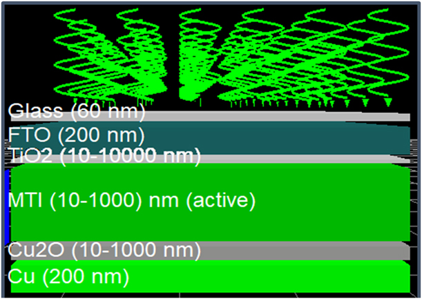
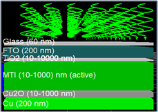
This research tackles the use of Pb and Ag/Au in the standard perovskite device structure. In our work, in lieu of Pb, we are using Sn to showcase the full functionality of the cell. We are also using Cu2O as an HTL (as opposed to the more common Spiro OMeTAD or P3HT), which can be reduced to form Cu as the metal for the counter-electrode. Through simulation studies, we have optimized on the active (perovskite) layer thickness to give the best efficiency. Figure 1 depicts the solar cell device architecture utilized in this simulation. Critical analyses of solar performance parameters—short-circuit current (J sc), open circuit voltage (V oc), and fill factor (FF)—are done to showcase performance impact, as this layer is modulated through a range of thickness values. Importantly, these trends are compared against a standard Pb-based perovskite device that is used as control; this device has the standard HTL (Spiro OMeTAD/P3HT) and Ag counter-electrode. These trends and comparisons provide keen insight into charge transfer kinetics within the device, paving the way to optimal experimental setups for fabricating efficient, non-toxic, and cheap perovskite devices.
The Sn-based perovskite with Cu2O HTL and Cu back-contact solar cell device architecture, with each critical layer optimized in thickness through the value range shown.

Results and discussion
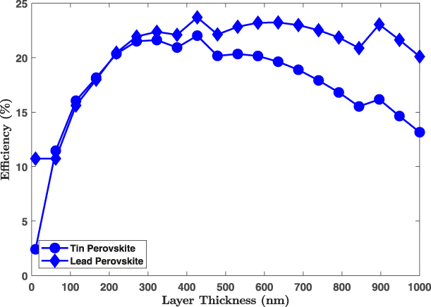
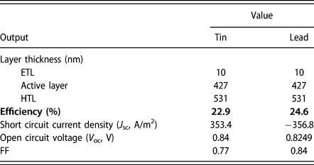
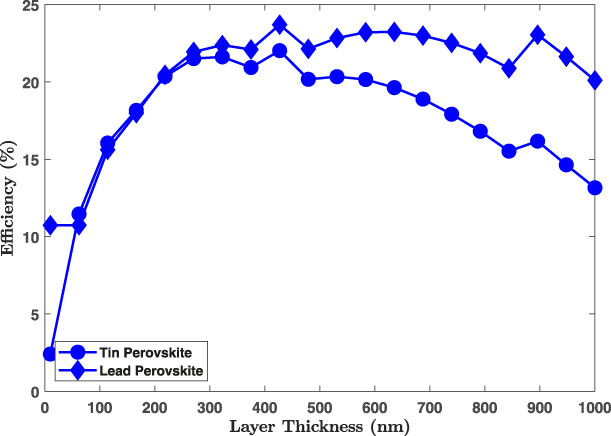
In this study, as mentioned earlier, we have focused on the active (perovskite) layer. There was a visible trend and peak within the data that signified the maximum cell efficiency achieved by modulating the thickness of just this layer. Figure 2 illustrates this behavior, while Table I lists out the key output parameters of the highest efficiency cells. It is interesting to note that both devices show similar behavior, with a notable peak in efficiency at 427 nm; beyond 427 nm, both devices show an overall downward trend.
Cell efficiency as a function of perovskite layer thickness.
Output of maximum efficiency cells.
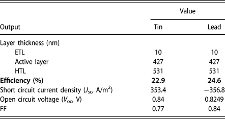
It is important to showcase that the maximum efficiency for the Sn perovskite/Cu2O HTL/Cu back-contact device at 22.9% is comparable to the 24.6% of the Pb perovskite/Spiro HTL/Ag back-contact device, providing encouragement for a host of research options to pursue to enhance the performance of the physical Sn perovskite device. The below discussions on J sc, V oc, and FF kinetics provide further insight into the performance of the two devices.
J sc kinetics
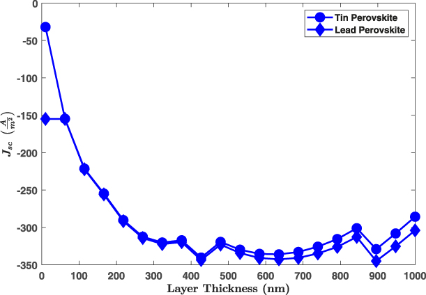
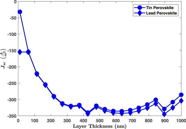
Figure 3 shows the J sc trends for the two devices. The two trends are almost identical, with the Sn perovskite/Cu2O HTL/Cu back-contact device trailing the Pb perovskite/Spiro HTL/Ag back-contact device slightly; post 500 nm, the Sn perovskite device trails the Pb perovskite more obviously. In general, with increasing film thickness, while more electron–hole pairs are created, defects and recombination centers within the film matrix also increase; these two competing forces typically lead to a bell curve trend [Reference Ahmed, Du Pasquier, Asefa and Birnie11, Reference Ahmed, Du Pasquier, Birnie and Asefa12]. This is what we see in Fig. 3 as well. It is certainly plausible that the Pb perovskite’s inherent higher electron/hole density of states and mobility contribute to these (slightly) better values than that of Sn. The Sn perovskite layer also has a higher defect density that its Pb counterpart, but the impact of an initial high density of defects (prior to solar irradiation) is still not understood well.
J sc as a function of perovskite layer thickness.
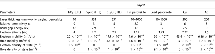
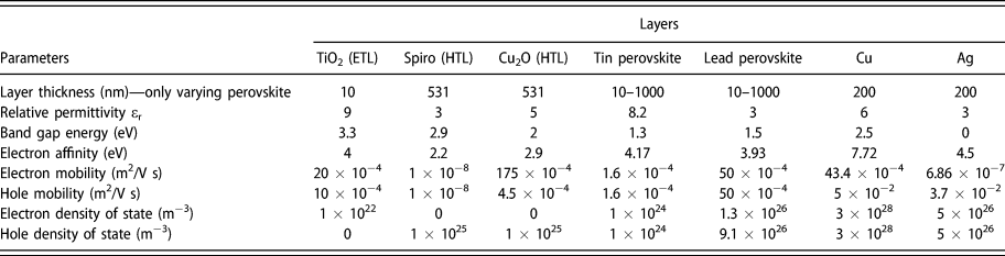
It is important at this junction to critically examine the Table II parameters of the other layers. The hole mobility of Cu2O is 4 orders of magnitude higher than that of its counterpart (Spiro), promising more efficient transfer of holes in the Sn-based device compared with the Pb-based device. In addition, the Cu2O to Cu differential in electron affinity is 4.82 eV, which is more than twice that of the counterpart device (2.3 eV for the Spiro/Ag differential), which again indicates quicker charge extraction for the Sn-based device. It appears that even though these obvious advantages exist for the Sn perovskite/Cu2O HTL/Cu back-contact device over the Pb perovskite/Spiro HTL/Ag back-contact device for holes to conduct more effectively, there are limitations that prevent them from being realized. These could include trap centers in and between the perovskite, Cu2O and Cu layers but importantly could involve various complex kinetics such as photoinduced ion migration, disorder, and hysteresis.
GPVDM parameter values extracted carefully from literature.
The above results become relevant in light of the phenomena of photo-brightening and photoinduced segregation found through photoluminescence (PL) microscopy [Reference deQuilettes, Zhang, Burlakov, Graham, Leijtens, Osherov, Bulovic, Snaith, Ginger and Stranks13]. It has been shown that light-soaking preferentially brightens regions with higher trap state densities (grains and grain boundaries) and include a redistribution in local emission intensities. Chemical imaging results reveal both lateral and vertical migration of iodine from illuminated areas, suggesting a redistribution process to homogenize the film content of the halide species. Additionally, with time, new concentration gradients may arise to cause ions to cluster or disperse, making the dynamics more complicated. Our current effort to modulate the perovskite layer thickness is critically affected by this photo-brightening and photoinduced segregation phenomena as it manifests through the 3D matrix of the perovskite. The authors aim to investigate the exact kinetics through their experimental work (underway), with the goal to elucidate the differences behind what simulations predict with what experiments reveal. As an example, spectroscopic and polarimetric electric field–induced second harmonic, together with second harmonic generation (SHG), are being used to map out electric fields around the electrodes and the ETL and HTL. The aim here is to understand behavior in terms of interfacial electrode or layer polarization and the impact on ion migration, halide redistribution, and hysteresis.
V oc kinetics
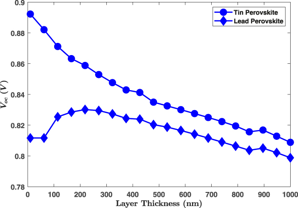
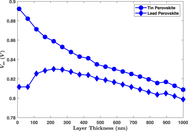
Figure 4 highlights the V oc trends for the Sn perovskite/Cu2O HTL/Cu back-contact device versus the Pb perovskite/Spiro HTL/Ag back-contact device. Both show a downward trend in V oc as a function of thickness; this is to be expected. In general, the decreasing V oc with increasing thickness dependence is found to derive from two factors; first, charge recombination sites are distributed throughout the film, enabling more charges to recombine in thicker films before influencing the potential at the electrodes, and second, the average optical power density within the film reduces with increasing film thickness [Reference Snaith, Schmidt-Mende, Grätzel and Chiesa14]. While both Sn and Pb have similar values in V oc (between 0.8 and 0.9 V) as the film thickness varies from 0 to 1000 nm, it is interesting to observe a few items. First, the Sn-based device has a better V oc value at every thickness than it is Pb counterpart; second, while the Pb perovskite shows a fairly constant V oc, with gradual decrease with increasing film thickness, the Sn-based device shows a sharp fall in the V oc with increasing film thickness. While the band gap of Sn perovskite (1.3 eV) can explain its intrinsic advantage over Pb perovskite (1.5 eV) in having higher optical power density within the cell by allowing more photons (density) to be captured, the recombination kinetics again seem to play a much more dramatic role in the Sn-based device as the film thickness increases and the V oc falls sharply. As the active layer thickness increases, defect centers increase as well, leading to higher electron and hole recombination. Last, it is important to stress that the Fermi level of a given device—effectively, its V oc—is strongly influenced by the J sc. “J sc kinetics” section’s discussion regarding the J sc kinetic comparison of the two devices, therefore, becomes relevant here as well.
V oc as a function of perovskite layer thickness.
To understand better our results in V oc, exploring ion migration and trap state density once again becomes critical. Through PL microscopy, it has been shown that the PL intensity of a standard Pb-perovskite film stabilizes after a few minutes [Reference deQuilettes, Zhang, Burlakov, Graham, Leijtens, Osherov, Bulovic, Snaith, Ginger and Stranks13]. What is also critically seen is a corresponding temporal rise and stabilization in open-circuit voltage when the film is used in a full operational device. It has been also proven that these kinetics can be explained with electronic sub-gap states. Interestingly, the extracted trap densities exhibit an inverse dependence with PL intensity. Under illumination, the trap density can reduce by an order of magnitude, along with increased emission and device photovoltage. The analyses reveal an activation energy for the ion migration process, the significance of which is still not well understood. Our investigation to optimize the perovskite layer thickness—focusing specifically on V oc in this section—is critically impacted by the kinetics of trap densities together with ion migration as it manifests through the 3D matrix of the perovskite. As noted previously, the authors’ goals include experimental investigation (underway) to correlate with the simulation results.
FF kinetics
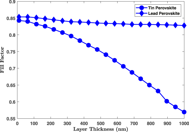
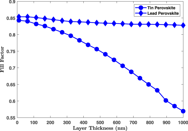
Figure 5 shows the FF trends for the Sn perovskite/Cu2O HTL/Cu back-contact device versus the Pb perovskite/Spiro HTL/Ag back-contact device. Qualitatively speaking, the FF is an indication of how effectively electron–hole pairs transport through the cell without loss (via recombination). The FF trends show a stark difference between the two materials: while the Pb-based cell shows a minimal degradation in FF values with film thickness, the Sn-based cell shows a drastic fall. It appears that this behavior is in line with our observations and conclusions from the J sc and V oc trends: Sn-based cells exhibit more intrinsic defects and recombination centers than their Pb-based counterparts. For the device stack-up, each layer—along with its interfacial contacts—is critical in influencing the overall FF kinetics. Together with this, as mentioned before, the motion of charge carriers can be influenced by trap state kinetics, photoinduced ion migration, disorder, and hysteresis.
FF as a function of perovskite layer thickness.
For the discussion of FF kinetics, the manner in which hysteresis manifests in the solar cell is particularly important. It has been shown that the J–V responses of perovskite cells demonstrate anomalous dependence on the voltage scan direction/rate/range, voltage conditioning history, and device configuration [Reference Chen, Yang, Priya and Zhu8]. Non-steady-state photocurrents associated with capacitive effects have been associated with electrode polarization at perovskite/electrode interfaces caused by interfacial phenomena, such as electric or ionic charge accumulation at the interface of the perovskite thin film. This could be well due to the presence of defects at these locations. A giant photoinduced dielectric permittivity can lead to an observed large low-frequency capacitance and a slow decay process for perovskite solar cells. These interfacial electrons and holes can not only enhance the polarization density but also modulate the band structure at the interface. By increasing the layer thickness, we effectively increased the 3D film matrix, extending out the space for hysteresis to play out; the fact that FF stays constant (as a function of film thickness) for the Pb-based device is impressive. For the Sn-based device, however, the poor FF trend alludes to adverse impacts on carrier transport due to interfacial charge accumulation leading to capacitive and hysteresis effects. This insight gleaned through our simulation work is critical in experimental work to counteract these effects, especially through the use of passivation layers at interfaces.
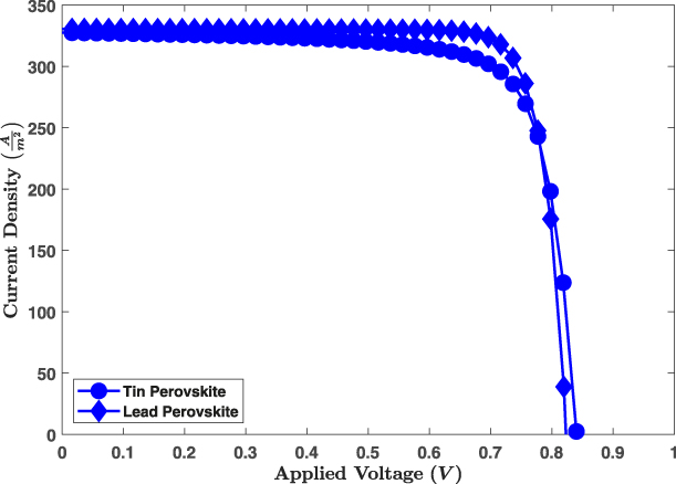
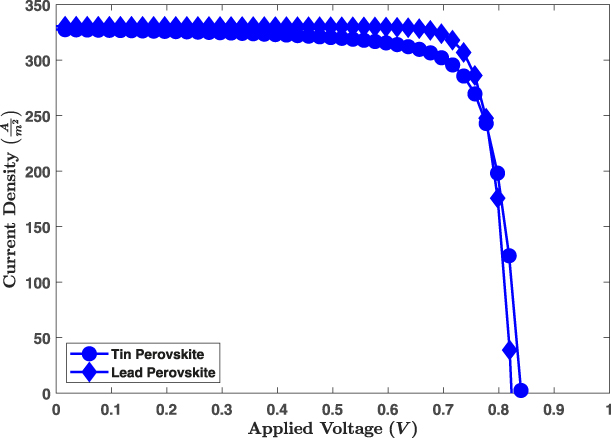
As an upshot to the discussion above, the typical J–V curve of the highest performing Sn-based device compared with its Pb counterpart is illustrated in Fig. 6. It becomes relevant to note here that experimentally, Sn-based perovskite films show poorer quality (i.e., with higher defect centers) than Pb-based films; the solubility of Sn halides and the controlled preparation of the selected crystal phases in particular are challenging [Reference Sani, Shafie, Lim and Musa15]. The notion that this in turn leads to lower efficiencies of Sn-based devices with respect to Pb is verified through our simulations and conclusions. All the performance parameters—V oc, J sc, and FF—of Sn-based films (in comparison with their Pb counterparts) indicate higher recombination or trap centers of the poorer quality films. What our results do show, however, are much higher values of the performance parameters, and therefore of the overall efficiency, of simulated results compared to current experimental numbers of Sn-based devices. This is promising in that it showcases the potential to make improvements on current Sn-based devices, in particular of fabricating better-quality films with fewer recombination centers.
J–V curve of the highest efficiency Sn perovskite device compared with a Pb one.
Conclusions
Using general-purpose photovoltaic device model (GPVDM), we have simulated the operation and functionality of a working Sn perovskite/Cu2O HTL/Cu back-contact device versus a standard Pb perovskite/Spiro HTL/Ag back-contact device. The results are extremely promising in that they showcase comparable cell efficiencies, with the Sn perovskite/Cu2O HTL/Cu back-contact device showing a highest 22.9% efficiency (J sc of 353.4 A/m2, V oc of 0.84 V, FF of 0.77) at 427 nm active layer thickness compared to 24.6% of the standard Pb perovskite/Spiro HTL/Ag back-contact device (J sc of 356.8 A/m2, V oc of 0.82 V, FF of 0.84) at the same active layer thickness. A deeper study of each of the J sc, V oc, and FF kinetics reveals that the Sn perovskite/Cu2O HTL/Cu back-contact device has intrinsic advantages of higher HTL hole mobility, combined with greater interfacial electron affinity differential, and could perform better by reducing the defect density/recombination centers both within each layer matrix and in the interfacial contacts.
Methodology
The GPVDM is a free online platform for simulating photovoltaic behavior, given input parameters (electrical and optical) for device layers [16]. The model uses a finite difference approach to solve both electron and hole drift-diffusion equations in position space to describe the movement of charge within the device. At each mesh point in position space, a set of carrier trapping and escape equations are solved in energy space. Recombination can occur by free-to-trap Shockley–Read–Hall (SRH) type recombination.
SRH theory describes the rates at which electrons and holes become captured and escape from the carrier traps. Charge carriers can give up their energy in collisions with the physical entity that gives rise to a localized level and become trapped by it. The trapping of an electron followed by the trapping of a hole completes the recombination. While details of the modeling can be found on the software platform and other sources [Reference Mackel and Mackenzie17, Reference Erwin, MacKenzie and Bardhan18, Reference Hume, Monks, Pop, Davies, Mackenzie and Amabilino19, Reference Wang, Li, Mackenzie, Wen, Liu, Ma, Wang, Tian and Ruan20, Reference Du, Wang and Zhu21], we provide below the core device physics for the cell functionality.
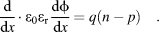
The model uses electronic levels defined as the highest occupied molecular orbital and lowest unoccupied molecular orbital energies, and the contacts are considered to consist of planes at x = 0 and x = d, where the boundary conditions are applied. Poisson’s equation [Eq. (1)] is used to model the space charge–dependent potential profile across the device; q is the charge on an electron, ε0 the permittivity of free space, εr the relative permittivity of the medium, n the total electron density (n = n free + n trap), and p the total hole density (p = p free + p trap):
 $${{\rm{d}} \over {{\rm{d}}x}} \cdot {\varepsilon _0}{\varepsilon _{\rm{r}}}{{{\rm{d}}\phi } \over {{\rm{d}}x}} = q\left( {n - p} \right)\quad .$$
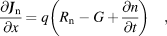
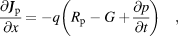
Furthermore, charge transport in the device is enumerated by the bipolar carrier continuity equations [Eqs. (2) and (3)] (ensuring charge conservation in the device) in 1D and time space:
 $${{\partial {{\bi{J}}_{\rm{n}}}} \over {\partial x}} = q\left( {{R_{\rm{n}}} - G + {{\partial n} \over {\partial t}}} \right)\quad ,$$
 $${{\partial {{\bi{J}}_{\rm{p}}}} \over {\partial x}} = - q\left( {{R_{\rm{p}}} - G + {{\partial p} \over {\partial t}}} \right)\quad ,$$
where J n,p are the electron and hole current flux densities, and R and G are the net recombination and generation rates per unit volume.
The carrier balance equation [Eq. (4)] consolidates the electron and hole capture and escape rate kinetics; for each trap level, the below equation is solved, thereby giving each trap level an independent quasi-Fermi level.
 $${{\partial {n_{\rm{t}}}} \over {\partial t}} = {r_{{\rm{ec}}}} - {r_{{\rm{ee}}}} - {r_{{\rm{hc}}}} + {r_{{\rm{he}}}}\quad ,$$
where r ec describes the rate at which electrons become captured into the electron trap, r ee is the rate which electrons can escape from the trap back to the free electron population, r hc is the rate at which free holes get trapped, and r he is the rate at which holes escape back to the free hole population.
Last, momentum conservation is maintained through the bipolar drift diffusion equations below:
 $${{\bi{J}}_{\rm{n}}} = q{\mu _{\rm{e}}}n{{\partial {E_{\rm{c}}}} \over {\partial x}} + q{D_{\rm{n}}}{{\partial n} \over {\partial x}}\quad ,$$
 $${{\bi{J}}_{\rm{p}}} = q{\mu _{\rm{h}}}p{{\partial {E_{\rm{c}}}} \over {\partial x}} + q{D_{\rm{p}}}{{\partial p} \over {\partial x}}\quad ,$$
where μe and μh are the charge density–dependent electron and hole mobilities, respectively, and D n,p are the electron and hole diffusion coefficients.
Figure 1 shows the planar heterojunction architecture of a Sn-based (non-Pb) perovskite—CH3NH3SnI3—solar sell with Cu2O as HTL and Cu as back-contact. The layer configuration adopted in this simulation is glass/FTO/ETL (TiO2)/CH3NH3SnI3/HTL/Cu. Thicknesses of the various cell layers are modulated to find optimal values (Fig. 1); for the purpose of this research, we emphasize the optimization of the active perovskite layer. Table II shows the key electrical parameters used for the simulation; the Sn perovskite, Cu2O and Cu values were chosen carefully from literature, with multiple sources listing exact values Reference Umari, Mosconi and De Angelis[22, Reference Chen, Huang, Ma, Cao and He23, Reference Noel, Stranks, Abate, Wehrenfennig, Guarnera, Haghighirad, Sadhanala, Eperon, Pathak, Johnston, Petrozza, Herz and Snaith24, Reference Hao, Stoumpos, Cao, Chang and Kanatzidis25, Reference Minemoto and Murata26, Reference Kemp, Labelle, Thon, Ip, Kramer, Hoogland and Sargent27, Reference Minemoto and Murata28, Reference Minemoto and Murata29, Reference Liu, Zhu and Wei30, Reference Leijtens, Bush, Prasanna and McGehee31, 33]. It is important to note that the perovskites values are of 3D Pb and Sn perovskites. While it is true that having 2D/3D mixes of perovskites leads to enhanced crystallinity and thereby better p-doping and charge carrier density, the aim here is to make 1:1 comparison with the most generic film composition of either metal perovskite. By modulating the thickness, we aim to showcase how we impact performance of the Sn versus the Pb device by spatially increasing the region for the various parameters—density of states, mobilities, trap densities, etc.—to work in. As mentioned earlier, this will in turn provide keen understanding into charge transfer kinetics within the device.
GPVDM’s standard Pb-based perovskite values, together with those for glass, FTO, TiO2, Spiro, and Ag, are used here Reference Umari, Mosconi and De Angelis[22, 33]. The thicknesses of glass (SiO2), FTO contact, and Ag or Cu contact are set to be 60, 200, and 200 nm, respectively; these are standard cell stack values and set as initial values in the software.
Acknowledgments
This work was supported by the Clean Energy Grant from SUNY Buffalo State.