Introduction
In contrast to cements and glasses, the essence of a semiconductor is the manipulation of electron transport. Reference Chelikowsky and Cohen1 One may question the relevance to semiconductors of the Phillips–Thorpe inspired molecular rigidity concepts described in the Introductory article of this issue. Reference Phillips and Thorpe2,Reference Micoulaut3 However, many key transitions in the semiconductor electronic structure bear striking similarities to the percolation and mechanical rigidity transitions exhibited in glassy and other noncrystalline solids. Reference Micoulaut3 As we illustrate in this article, such electronic transitions can be important in optimizing semiconductors for specific applications and, in some cases, offer the potential to realize new devices that could further revolutionize the world. Reference Park, Maeng, Kim and Park4,Reference Nikonov and Young5 We additionally demonstrate how rigidity percolation plays a more direct role in insulating high- and low-dielectric-constant (high-/low-k) materials. This is important to achieve voltage-controlled electronic transport in commercial semiconductor devices that have already made a significant technological impact. Reference King, Simka, Herr, Akinaga and Garner6
Semiconductor metal–insulator transitions
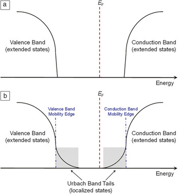
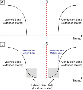
As their name implies, semiconductors are neither ideal conductors nor insulators. However, the ability to tune their conductivity over many orders of magnitude and manipulate the majority carrier type via the deliberate introduction of impurities (doping) has made them indispensible. Reference Chelikowsky and Cohen1 The unique properties exhibited by semiconductors are a result of their electronic structure—the existence of a bandgap with most of the allowed electronic states in the lower valence band being occupied and only a few allowed states in the upper conduction band being occupied. Whether a state is full, partially filled, or empty is governed by Fermi–Dirac statistics and is described by the Fermi level (E F), which is defined as the energy level where there is a 50% probability of occupancy at any given time (see Figure 1a). Reference Solymar and Walsh7 What makes semiconductors so useful and interesting is the possibility of adjusting E F and hence conductivity via the intentional introduction of impurities or defects (dopants) to create states just above or below the conduction and valence bands, respectively.
Schematic illustration of bands of allowed electron energy levels and their occupancy in (a) a crystalline semiconductor, and (b) an amorphous semiconductor, illustrating Urbach band tails and the mobility edge.
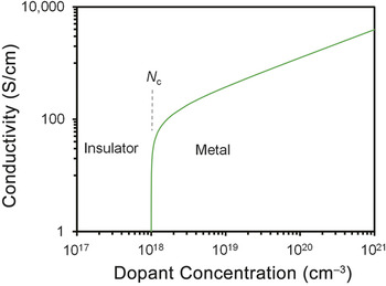
In ideal conditions, semiconductors are perfect insulators at cryogenic temperatures due to lack of thermal activation of electrons into the conduction band. At such temperatures, dopant states in low concentrations remain localized and are unable to contribute to conductivity. However, as the dopant concentration is increased, a critical concentration is eventually reached where the dopant states become delocalized and form a percolating path of extended states. Reference Holcomb and Rehr8,Reference Zallen9 At this point, the semiconductor switches from exhibiting insulating to metallic characteristics (see Figure 2 ) and leads to our first connection with rigidity percolation theory. As this transition is approached from the metallic side, a scaling theory of localization predicts that conductivity should decrease in a continuous manner according to the relation:
 $$\sigma \left( 0 \right) = {\sigma _0}{\left[ {\left( {N - {N_c}} \right)/{N_c}} \right]^\nu },$$
where σ(0) is the conductivity extrapolated to zero temperature, σ0 is a prefactor, N is the doping concentration, N c is the critical doping concentration, and ν is a critical exponent that has been experimentally determined to be 0.5 or 1, depending on the dopant type. Reference Ito, Haller, Beeman, Hansen, Emes, Reichertz, Kreysa, Shutt, Cummings, Stockwell, Sadoulet, Muto, Farmer and Ozhogin10 Equation (1) is directly analogous to the flexible/stressed-rigid mechanical transition predicted by the Phillips–Thorpe theory, Reference Phillips and Thorpe2,Reference Micoulaut3 where N and N c may alternatively be represented by the mean network coordination (〈r〉) and critical coordination (〈r〉c), respectively. Reference Phillips and Thorpe2
Illustration of a hypothetical metal–insulator transition in a semiconductor with N c = 1018/cm3, σ0 = 125 S/cm, and ν = 0.5. Reference Ito, Haller, Beeman, Hansen, Emes, Reichertz, Kreysa, Shutt, Cummings, Stockwell, Sadoulet, Muto, Farmer and Ozhogin10

The dramatic change in resistance exhibited in such metal–insulator transitions has for many decades been recognized as the basis for a potential memory-storage or digital-logic device. Reference Strukov and Kohlstedt11 More recently, resistance switching devices have emerged that exhibit similar metal–insulator type transitions. These devices operate based on the voltage-controlled formation and destruction of a percolating path of extended metallic or vacancy defect states in a semiconducting or insulating medium. Such devices are of extreme interest as a potential means for continued Moore’s Law dimensional scaling and extending beyond the end of the roadmap for the current complementary metal oxide semiconductor (CMOS) devices that have dominated the microelectronics industry for the past several decades. Reference King, Simka, Herr, Akinaga and Garner6,Reference Solymar and Walsh7
Amorphous semiconductors, such as a-Si:H, also exhibit a related localized–extended transition whose unique origin stems from disorder. Although short-range order typically exists in amorphous semiconductors, a lack of long-range periodicity leads to a broadening of valence- and conduction-band edges that manifests in the form of band tail states, also known as Urbach states (see Figure 1b). Reference Drabold, Li, Cai and Zhang12 These band tail states arise from the topological disorder (i.e., deviations in bond lengths and angles) present in amorphous semiconductors, which induces localized states that decay exponentially into the bandgap to form band tails, whose width is defined as the Urbach energy. The boundary between the delocalized (extended) band states and the localized band tail states in an amorphous semiconductor is typically referred to as a “mobility edge,” and the resulting “mobility gap” is analogous to the bandgap in crystalline solids.
Electrons above (or holes below) the mobility edge can participate in band transport, whereas electrons below (or holes above) are effectively trapped. The latter may participate in hopping-based transport, where the movement of charge carriers occurs via tunneling between localized states, or play a role in multiple-trapping-based transport, where the movement of charge carriers occurs via band states, but is interrupted by trapping in localized states. In either case, a marked decrease in mobility relative to pure band transport is observed. Reference Baranovski13 Thus, depending on the specific material/experimental parameters (e.g., Urbach energy, bandgap, temperature, electric field), a sample may exhibit a range of possible transport behavior, and direct links between Urbach band tail widths, electron mobility, and performance have been established in a-Si:H, a-Si x C1–x :H, and related semiconducting devices. Reference Mahan, Carapella, Nelson, Crandall and Balberg14,Reference Sato, King, Lanford, Henry, Fujiseki and Fujiwara15 Perhaps most interestingly, it has been shown that disorder and electronic structure parameters, including Urbach energy, Tauc slope parameter, B (typically considered a measure of disorder that can be extracted from a Tauc analysis of the absorption coefficient plot), and bandgap can be tuned as a function of stoichiometry (and corresponding network coordination), Reference Ambrosone, Basu, Coscia and Fathallah16 including a possible transition analogous to the rigidity transition in network glasses, Reference Nordell, Karki, Nguyen, Rulis, Caruso, Purohit, Li, King, Dutta, Gidley, Lanford and Paquette17 which opens the door to unique possibilities for tuning charge transport in amorphous semiconductors.
Amorphous solids and resistance percolation
Arguably the most direct connection between charge transport and topological constraint theory can be found if electrical conduction is viewed through the lens of percolation theory, Reference Zallen9 where individual bonds are treated as discrete resistors, as is appropriate for a hopping conduction mechanism in amorphous solids. Reference Baranovski13 Starting with a fully connected network of resistors with discrete conductivity, the network conductivity decreases (i.e., the resistance increases) as resistors are removed from the network and effectively replaced by a path of infinite resistance. As with mechanical rigidity transitions, a certain critical percentage of resistors (or bonds) exists below which the current goes to zero and the entire network effectively represents an open circuit. Reference Zallen9 The critical bond/resistor density to support finite conductivity has been computationally determined for a number of lattices. For a tetrahedral lattice, relevant to most crystalline and amorphous semiconductors, the critical resistor/bond density has been determined to be ∼39%. Reference Vyssotsky, Gordon, Frisch and Hammersley18 This corresponds to a critical coordination 〈r〉c of ∼2.4, Reference Ziman19 in excellent agreement with the value of 2.4 predicted for mechanical rigidity percolation through a tetrahedral lattice. Reference Phillips and Thorpe2,Reference Micoulaut3
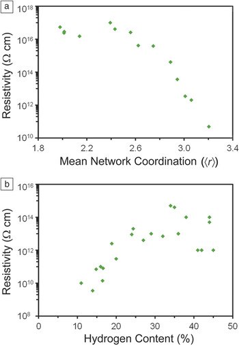
We recently experimentally demonstrated the existence of such a threshold in a-SiC:H semiconducting materials, where resistance was observed to increase steadily with hydrogen content and plateau at values of ∼46%. Reference Pomorski, Bittel, Cochrane, Lenahan, Bielefeld and King20,Reference King, Bielefeld, Xu, Lanford, Matsuda, Dauskardt, Kim, Hondongwa, Olasov, Daly, Stan, Liu, Dutta and Gidley21 As will be discussed further, hydrogen has an effective coordination of one and in amorphous solids acts as a network modifier (similar to alkali metals such as sodium and potassium in silicate glass chemistry Reference Phillips and Thorpe2,Reference Micoulaut3 ). The addition of hydrogen thus has the effect of reducing 〈r〉 for the a-SiC:H system. As shown in Figure 3a, the plateau in a-SiC:H resistance observed at 46% H corresponds to an 〈r〉 of 2.4, in excellent agreement with the prediction by topological constraint theory. Reference King, Bielefeld, Xu, Lanford, Matsuda, Dauskardt, Kim, Hondongwa, Olasov, Daly, Stan, Liu, Dutta and Gidley21
(a) Electrical resistivity for a-SiC:H semiconducting dielectrics as a function of average bond coordination 〈r〉. Reference King, Bielefeld, Xu, Lanford, Matsuda, Dauskardt, Kim, Hondongwa, Olasov, Daly, Stan, Liu, Dutta and Gidley21 (b) Electrical resistivity for supermolecular solid a-B x C:H as a function of hydrogen content. Reference Nordell, Karki, Nguyen, Rulis, Caruso, Purohit, Li, King, Dutta, Gidley, Lanford and Paquette17 Both illustrate plateaus in electrical resistance that correspond to the critical average bond coordination/resistor connectivity predicted by topological constraint theory for electrical conductivity percolation in a resistor lattice.

Similar thresholds in electrical resistivity have also been observed in other amorphous solids. One interesting example is semiconducting B4C, which is a supermolecular solid composed of B12-based icosahedra containing carbon, forming both intra- and inter-icosahedral linkages. Reference Nordell, Karki, Nguyen, Rulis, Caruso, Purohit, Li, King, Dutta, Gidley, Lanford and Paquette17 The addition of substantial amounts of hydrogen to make a-B x C:H disrupts the B12 linkages, where terminal hydrogen atoms act as network modifiers as in a-SiC:H. As shown in Figure 3b, a similar plateau in resistivity in a-B x C:H is observed at hydrogen content starting at 30–35%. Reference Nordell, Karki, Nguyen, Rulis, Caruso, Purohit, Li, King, Dutta, Gidley, Lanford and Paquette17,Reference Nordell, Nguyen, Keck, Dhungana, Caruso, Lanford, Gaskins, Hopkins, Merrill, Johnson, Ross, Henry, King and Paquette22 While 〈r〉c for a supermolecular icosahedral network has yet to be determined, the likely underlying role of topological constraint theory in Figure 3b seems clear.
Semiconductor gate dielectrics (SiO2, a-SiN x :H, and high-k)
A key component of modern-day field-effect-transistor (FET) devices is a highly insulating dielectric that isolates the semiconducting material from a metallic electrode and allows voltage control of electrons (or holes) through a semiconducting channel formed beneath the dielectric. So-called “gate” dielectrics must fulfill a number of stringent criteria, including exhibiting low leakage currents, high breakdown voltages, and a low density of localized interface states that can reduce carrier mobilities in the semiconductor channel and impede device voltage control. Reference Solymar and Walsh7 Such interface states are typically the result of unsatisfied dangling bonds at the semiconductor surface and related dangling bond defects within the gate dielectric. Reference Chelikowsky and Cohen1 Minimizing such defects is a seemingly daunting task given the large differences in atomic density, bond lengths, bond angles, and general lattice mismatch between typical semiconductor and gate dielectric materials.
For the prototypical semiconductor/gate dielectric Si/SiO2 interface, substantial mismatches exist in atomic density (40%), Si–Si interatomic distances (Si = 0.235 nm, SiO2 = 0.305 nm), 〈r〉 (Si = 4, SiO2 = 2.67), and linear coefficient of thermal expansion (Si = 2.5 × 10⁻⁶ C–1, SiO2 = 0.5 × 10⁻⁶ C–1). Reference Lucovsky and Phillips23 These mismatches create significant interfacial strain in both the Si channel (tensile) and SiO2 gate dielectric (compressive) that can serve to nucleate various interfacial defects and degrade device performance. Nevertheless, Si/SiO2 interfaces with remarkably low densities of defect states (1010/cm2) are currently routinely achieved in silicon-based CMOS FET devices. Reference Lucovsky, Wu, Niimi, Misra and Phillips24 Interestingly, the ability to form Si/SiO2 interfaces with such low defect densities can be elegantly understood directly through topological constraint theory. Reference Phillips25
In the Introductory article of this issue, it was demonstrated that if both bond bending and stretching forces are present, the optimal 〈r〉*, which matches the number of constraints to the number of degrees of freedom for tetrahedrally bonded networks, is 2.4. However, for SiO2-based materials, 〈r〉* is generally considered to be 2.67 as the O-bond-bending forces are believed to be too weak to function as constraints at common SiO2 gate oxide growth temperatures. This larger 〈r〉* is essentially identical to the 〈r〉 for SiO2 and thus, the elastic compliance of the underconstrained SiO2 dielectric allows sufficient flexibility to self-assemble into a configuration that maximally passivates dangling bonds present at the semiconductor surface and simultaneously minimizes the formation of defects within its own structure. Reference Phillips25 This general rationale has also been shown to be applicable to many other combinations of semiconductors and gate dielectrics. For example, Lucovsky has shown Reference Lucovsky and Phillips26 that for a-Si:H/a-SiN x :H thin-film transistor devices commonly used in liquid crystal displays, optimal a-Si:H channel mobilities and device performance are achieved with a-SiN x :H gate dielectrics having a unique Si:N:H composition ratio of ∼0.3:0.4:0.3. Reference Lucovsky and Phillips26 This composition corresponds to an 〈r〉 of 2.7, which is essentially identical to that for SiO2 gate dielectrics and implies a similar flexibility for such a-SiN x :H dielectrics to adapt to the underlying overconstrained a-Si:H topology to minimize interfacial defects.
An additional example of the applicability of topological constraint theory to semiconductor/gate dielectric interfaces can be gained from examining the recent migration away from SiO2 as the gate dielectric in c-Si CMOS devices. This transition was driven primarily by the need to reduce the electrically equivalent oxide thickness (EOT) in CMOS devices while still maintaining a physical oxide thickness sufficient to minimize tunneling leakage through the gate dielectric into the channel. This was accomplished by adopting new gate dielectric materials with high dielectric constant values approaching 20–25. Reference King, Simka, Herr, Akinaga and Garner6 The primary high-k materials considered include Al2O3-, ZrO2-, and HfO2-based materials, which allow EOT scaling while preserving a physical oxide thickness of ∼1 nm. Reference Wilk, Wallace and Anthony27 From a constraint theory perspective, these are all highly overconstrained materials (〈r〉 > 3) that based on the preceding rationale would preclude the formation of a strain-free/low-defect-density interface with c-Si. Reference Lucovsky, Maria and Phillips28 Experimentally, this has been found to be the case: high-k dielectrics deposited directly on c-Si exhibit many orders of magnitude higher densities of interface defects. Reference Lucovsky and Phillips23 In order to successfully integrate high-k dielectrics in Si CMOS, it has been found necessary to incorporate a thin compliant SiO2 transition layer to minimize interfacial strain. Reference Lucovsky and Phillips23,Reference Lucovsky, Maria and Phillips28
Low-k metal interconnect dielectrics
Another key component of a highly integrated semiconductor-based microelectronic product is the miniaturized metal wiring needed to interconnect the millions to billions of transistors within each individual chip. Reference King, Simka, Herr, Akinaga and Garner6 This is achieved primarily by fabricating multiple layers of interconnected metal wiring inlaid in an insulating intralayer dielectric (ILD) on top of the planar transistor devices. In modern devices, the number of stacked metal layers is now in the range of 10–20 and, correspondingly, signal propagation delays in the interconnect are now approaching those of the transistor. Reference Grill, Gates, Ryan, Nguyen and Priyadarshini29 Since the metal interconnect delay is proportional to the product of the metal resistance and the ILD capacitance, significant research has been invested in finding ways to reduce both. For the latter, substantial efforts have been made to identify and implement so-called “low-k” dielectric materials with dramatically reduced values of dielectric constant relative to SiO2 (the default ILD in microelectronics for many decades). Reference Maex, Baklanov, Shamiryan, Iacopi, Brongersma and Yanovitskaya30 Low-k materials provide yet another example of the application of topological constraint theory in material optimization.
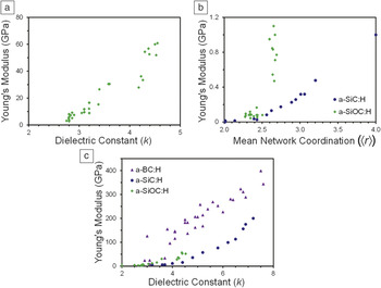
Modern-day low-k dielectric materials are created primarily via the deliberate insertion of terminal hydrogen bonds or organic groups into the network structure of SiO2. Low-k materials are thus nominally SiOC:H in composition and are sometimes referred to as carbon-doped oxides or, more accurately, as organosilicates. Reference Grill, Gates, Ryan, Nguyen and Priyadarshini29,Reference Maex, Baklanov, Shamiryan, Iacopi, Brongersma and Yanovitskaya30 One of the primary challenges with implementing low-k materials is their degraded mechanical properties relative to SiO2 that can be manifested via a variety of thermomechanical failures during fabrication and packaging. Reference Grill31 The severity of the low-k challenge becomes even more acute when one considers the direct correlation observed between reducing dielectric constant and ensuing reduced mechanical properties (see Figure 4a). Reference King32–Reference Pomorski, Bittel, Lenahan, Mays, Ege, Bielefeld, Michalak and King34 This trend has largely contributed to numerous delays by the microelectronics industry in implementing organosilicate materials with increasingly reduced values of dielectric constant and have caused some to refer to Figure 4a as the low-k “death curve.” Reference Nordell, Nguyen, Keck, Dhungana, Caruso, Lanford, Gaskins, Hopkins, Merrill, Johnson, Ross, Henry, King and Paquette22 Fortunately, the challenges associated with low-k dielectric materials can be understood directly through the concepts of topological constraint theory. Specifically, the deliberate replacement of bridging oxygen bonds in the SiO2 network with terminal H or CH x entities essentially amounts to topological engineering of the low-k network structure with the net effect of increasing H/CH x incorporation to reduce dielectric constant, which also reduces 〈r〉 and hence mechanical properties. Reference Grill31
(a) Young’s modulus versus dielectric constant for a series of organosilicate low-k dielectrics. Reference King32-Reference Pomorski, Bittel, Lenahan, Mays, Ege, Bielefeld, Michalak and King34 (b) Normalized nanoindentation Young’s modulus versus average bond coordination for a-SiOC:H and a-SiC:H dielectrics illustrating singularity at 〈r〉 predicted by constraint theory. Note: a-SiOC:H and a-SiC:H normalized to Young’s modulus of single-crystal 3C-SiC (440 GPa) and SiO2 Quartz (100 GPa), respectively. Reference King, Bielefeld, Xu, Lanford, Matsuda, Dauskardt, Kim, Hondongwa, Olasov, Daly, Stan, Liu, Dutta and Gidley21,Reference King32-Reference Pomorski, Bittel, Lenahan, Mays, Ege, Bielefeld, Michalak and King34 (c) Young’s modulus versus dielectric constant for a-B x C:H, a-SiOC:H, and a-SiC:H. Reference King, Bielefeld, Xu, Lanford, Matsuda, Dauskardt, Kim, Hondongwa, Olasov, Daly, Stan, Liu, Dutta and Gidley21,Reference Nordell, Nguyen, Keck, Dhungana, Caruso, Lanford, Gaskins, Hopkins, Merrill, Johnson, Ross, Henry, King and Paquette22

A key question for low-k materials, though, is whether mechanical properties go to zero as predicted by linear extrapolation in Figure 4a or bottom out at finite values. Research on rigidity percolation in low-k a-SiC:H and a-SiOC:H dielectrics has yielded some fundamental insights. Reference King, Bielefeld, Xu, Lanford, Matsuda, Dauskardt, Kim, Hondongwa, Olasov, Daly, Stan, Liu, Dutta and Gidley21,Reference King32 As shown in Figure 4b, a clear singularity exists at 〈r〉 = 2.4 for nanoindentation Young’s modulus for a variety of silicon-based dielectrics. Importantly, the plateauing of Young’s modulus at low but finite values for 〈r〉 < 2.4 is also clear.
A greater research question for low-k materials is whether it would be possible to break the low-k “death curve” and find materials where the 〈r〉 versus Young’s modulus correlation is shifted to the upper left portion of Figure 4a. Some hope has been recently realized through the identification of a-B x C:H as a promising low-k dielectric candidate. As shown in Figure 4c, such materials exhibit an order of magnitude higher Young’s modulus for a given value of dielectric constant relative to other silicon-based dielectrics. Reference Nordell, Nguyen, Keck, Dhungana, Caruso, Lanford, Gaskins, Hopkins, Merrill, Johnson, Ross, Henry, King and Paquette22 From a topological constraint theory perspective, it is also interesting to note that a plateau in Young’s modulus (of ∼20 GPa) is observed for a-B x C:H films with densities below ∼1.3 g/cm3. Reference Nordell, Nguyen, Keck, Dhungana, Caruso, Lanford, Gaskins, Hopkins, Merrill, Johnson, Ross, Henry, King and Paquette22 This suggests the existence of a similar critical threshold in 〈r〉 as for tetrahedral amorphous solids, and that low-density low-k films will retain a relatively high fundamental mechanical strength. The theoretical derivation of 〈r〉c for a supermolecular icosahedral-based network represents an area of active research and highlights the vibrancy of research in the field of molecular rigidity theory.
Conclusion
In this article, we illustrated how many interesting electrical and mechanical properties in disordered semiconductors, insulating dielectrics, and their interfaces can be easily understood and interpreted through topological constraint and percolation theories, which reduce the disorder-induced complexity of an amorphous system to a single critical density of states or mean network coordination 〈r〉. We hope this brief review of some aspects of percolation and topological constraint theory relevant to amorphous semiconductors and dielectrics sparks increased interest in the field and leads to a greater appreciation of the role they play in the structure–property relationships of amorphous materials.

Michelle M. Paquette is a research professor in the Department of Physics and Astronomy at the University of Missouri–Kansas City. She obtained her BSc degree in chemistry at the University of Guelph, Ontario, Canada, in 2006. She completed her doctoral work in chemistry, obtaining her PhD degree from the University of Victoria, British Columbia, Canada, in 2010. Her research focuses on the study of unusual semiconductor materials with an eye toward applications such as low-k dielectrics and solid-state neutron detection. Paquette can be reached by email at paquettem@umkc.edu.

Bradley J. Nordell is the laboratory manager at the Extreme Light Laboratory at the University of Nebraska–Lincoln, as well as a doctoral candidate in physics at the University of Missouri–Kansas City. He received his BSc degree from the University of Nebraska–Lincoln in 2010 and his MSc degree from the University of Missouri–Kansas City in 2012. His current research focuses on applying percolation theory to amorphous hydrogenated boron carbide for the optimization of the dielectric, electronic, and mechanical properties of this material as a next-generation low-k dielectric. Nordell can be reached by email at bnordell2@unl.edu.

Anthony N. Caruso is a professor of physics and Assistant Vice Chancellor for Research at the University of Missouri–Kansas City. He received his PhD degree in physics from the University of Nebraska–Lincoln in 2004 and was a research scientist at the Center for Nanoscale Science and Engineering at North Dakota State University until 2007. He is an associate editor of the journal IEEE Transactions on Nuclear Science and also holds federal appointments. Caruso can be reached by email at carusoan@umkc.edu.

Masanori Sato is a graduate student in the Department of Electrical and Electronic Engineering at Gifu University, Japan. He earned his undergraduate degree from Gifu University in 2013. He specializes in the real-time characterization of thin-film growth using spectroscopic ellipsometry. Sato can be reached by email at maka08404649@gmail.com.

Hiroyuki Fujiwara is a professor in the Department of Electrical, Electronic and Computer Engineering at Gifu University, Japan. He received his PhD degree from the Tokyo Institute of Technology, Japan. He was a research associate at The Pennsylvania State University from 1996 to 1998. In 1998, he joined the Electrotechnical Laboratory, Ministry of International Trade and Industry, Japan. In 2007, he became a team leader of the Research Center for Photovoltaics, National Institute of Advanced Industrial Science and Technology (AIST), Japan. Fujiwara can be reached by email at fujiwara@gifu-u.ac.jp.

Sean W. King is a senior technical contributor within Intel Corporation’s Logic Technology Development Division. He obtained a BS degree in materials engineering from the Virginia Polytechnic Institute and State University, and a PhD degree in materials science and engineering from North Carolina State University. His current research interests include high-k dielectrics, wide-bandgap semiconductors, 2D materials, resistive switching materials and devices, radiation-hardened materials, surface science, and nanoscale structure–property characterization. King can be reached by phone at 503-613-7547 or by email at sean.king@intel.com.