Introduction
With the rapid development of wireless communications, there is an urgent need for designing microwave filters with various behaviors. More studies have been conducted to achieve low-pass response of the filter as well as the bandpass behavior to satisfy the demands of recent wireless technologies with constrained specifications like small occupied area, high selectivity, enhanced roll-off rate, wide rejection band, and low passband insertion loss [Reference Boutejdar, Abd Ellatif, Ibrahim and Challal1–Reference Ibrahim, Mohamed and Ali4]. There are different techniques to achieve the desired filter behavior such as defected ground structures (DGSs) for achieving wide stopband behavior [Reference Han, Liu, Zhang, Mei, Chen, Hu and Yuan5, Reference Ouf and Anwer6] and also it can be used to miniaturize the filter structure [Reference Kumar and Kartikeyan7]. Moreover, the stepped impedance resonator technique can be utilized in designing bandpass filters (BPFs) for highly independent multiband behavior [Reference Firmansyah, Alaydrus, Wahyu, Rahardjo and Wibisono8], and for flexible bandwidth with an improved insertion loss [Reference Kicheol and Kim9]. The substrate-integrated wave technique was utilized in [Reference Yang, Bin You and Luo10] to achieve dual/triple passbands. In [Reference Sarbani and Moyra11], interdigital capacitors are used to achieve the desired bandpass behavior with an extended rejection band and it is also utilized in the design of a BPF to cover the ultra-wideband (UWB) frequency range from 3.1 to 10.6 GHz [Reference Verma, Moyra, Sarkar and Kumar12]. Two BPFs are introduced in [Reference Ibrahim, Ali and Abdelghany13, Reference Ibrahim, Ali and Abdalla14] based on the open-loop resonator technique for WLAN/WiMAX applications. Tunable filters are considered one of the demanded filters due to their vital role in adaptation to the requirements of wireless systems such as reconfigurable or cognitive systems. Recently, many tunable filters have been reported such as the reported Band stop filter (BSF) in [Reference Hamdalla M and M15] which is based on a tunable epsilon-shaped metamaterial using a lumped capacitor (connected in series) to achieve triple-band operation, also the same kind of lumped capacitors (connected in shunt) can shift the obtained bandpass behavior to the lower-frequency range causing a reduction in the filter size to more than 35% as in [Reference Boutejdar, Ibrahim and Ali16]. The reconfigurability of the suggested filters in [Reference Mohamed, El-Shaarawy, Abdallah and El-Hennawy17, Reference Mohamed, El-Shaarawy, Abdallah and El-Hennawy18] is carried out using PIN diodes to either obtain dual-mode behavior or control the notched band, respectively.
In this paper, a DGS-based low-pass filter (LPF) is introduced to achieve a larger frequency range up to 10 GHz and this is done by three etched DGS shapes from the ground plane which operated as band stop filters in the range from 10 to 18 GHz. Furthermore, two interdigital capacitors are inserted in the feedline of the aforementioned designed filter to obtain a dual passband behavior at 4.5 and 9 GHz. In order to achieve a wideband instead of the dual narrow bands when using two interdigital capacitors, two lumped capacitors are embedded and the exact values are chosen after carrying out a parametric study on capacitor values; finally two pairs of 1 pF capacitors are chosen to cover a larger frequency range starting from 1.9 to 10 GHz with a low-level return loss in the achieved passband range. Finally, the performance of each filter of the three suggested filters is validated experimentally and it was confirmed that the results of the fabricated filters and their simulated outcomes confirm the ability of the implemented filter to be incorporated in modern wireless devices due to their competitive specifications with the reported filters.
DGS BSF (Band stop filter)/LPF
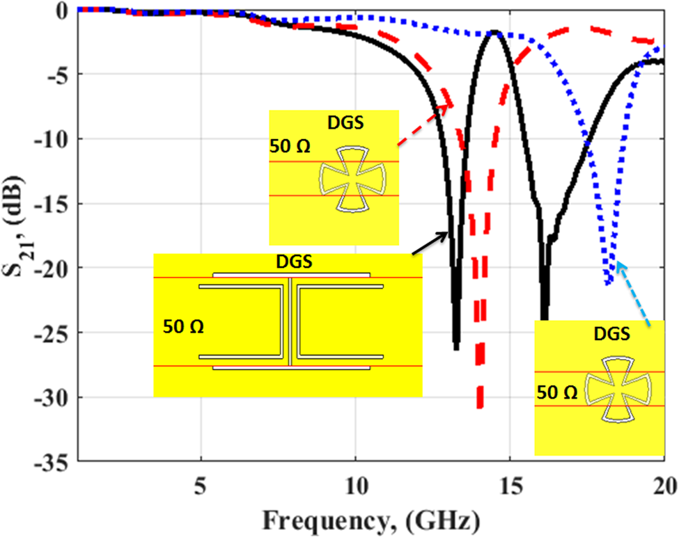
In this section, BSF/LPF based on DGS shapes is investigated. The DGS shapes are etched in the ground plane to achieve the proposed band-stop features. To achieve the proposed LPF from BSF, multiple attenuation poles should be used. So, different DGS shapes with different sizes should be used. Figure 1 shows the S 21 response of the DGS shapes. The fan-shaped with a larger size is etched in the ground plane while the microstrip line with 50 Ω is used on the other side of the substrate. The filter has band stop behavior with attenuation pole (fp) and 3-dB cut-off frequency (fc) corresponding to 14 and 11.7 GHz (the red-dashed line). Furthermore, to increase the attenuation poles in the stopband operation, DGSs with I-shaped and two backed C-shaped with smaller sizes are used as shown in Fig. 1. The filter has a band stop feature with two attenuation poles (fp) and 3-dB cut-off frequency (fc) corresponding to 13.25, 16, and 11.5 GHz for both bands (the solid black line). Finally, the smaller DGS with fan-shaped can be used to achieve band stop behavior with attenuation pole (fp) and 3-dB cut-off frequency (fc) corresponding to 18 and 16.2 GHz (the blue-dotted line). The parallel LC circuit can be used to model the DGS BSF. The values of the L and C can be extracted using the below equations [Reference Boutejdar, Ibrahim and Burte19, Reference Ibrahim, Abdalla and Ali20]:


S 21 response of different DGS shapes.

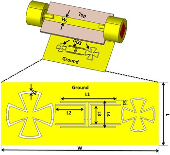
So, by combining the three DGS shapes as shown in Fig. 2, the LPF from BSF can be generated as shown in Fig. 3. The three-dimensional and two-dimensional views with the dimensions are shown in Fig. 2. The filter has three DGS-shaped etched on the ground of the substrate while a microstrip line with 50 Ω is printed on the top of the Roger 5880 substrate with ɛr = 2.2 and thickness of 0.8 mm.
DGS LPF configuration with L = 11 mm, W = 22 mm, S 1 = 0.2 mm, S 2 = 0.1 mm, L 1 = 5.5 mm, L 2 = 2.95 mm, L 3 = 1.8 mm, L 4 = 2.4 mm, and Wf = 2.4 mm.

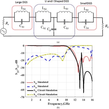
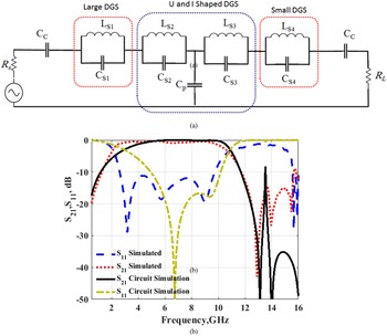
DGS LPF equivalent circuit analysis. (a) Equivalent circuit model with LS 1 = 0.41 nH, CS 1 = 0.315 pF, LS 2 = 0.35 nH, CS 2 = 0.42 pF, LS 3 = 0.66 nH, CS 3 = 0.147 pF, LS 4 = 0.186 nH, CS 4 = 0.418 pF, CP = 0.316 pF. (b) S-parameter responses of the EM simulation and circuit simulation.

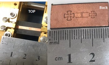
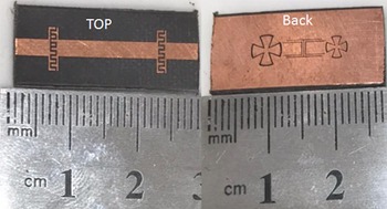
The equivalent circuit model of the proposed LPF is shown in Fig. 3(a). As discussed before the DGS element can be modeled as a parallel LC circuit, so four LC circuits are used to model the DGS BSF shape as discussed above. The comparison between the S-parameter responses of the electromagnetic (EM) and circuit simulation is shown in Fig. 3(b). It is obvious that the filter is LPF with passband operation up to 10.6 GHz and has wide stopband operation up to 16 GHz because of the multiple attenuation poles achieved by the DGS resonators. Also, a good trend between the two results is achieved. The proposed filter is fabricated and tested, and its fabricated photograph is illustrated in Fig. 4.
Top and back views of the DGS LPF fabricated prototype.

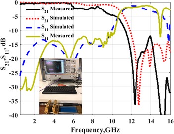
The filter is tested using a test feature kit instead of soldering two SMA connectors as shown in Fig. 4. The proposed filter is tested using a Rohde & Schwarz ZVA 67 vector network analyzer using 50-Ω ports to extract the filter's S-parameter response as shown in Fig. 5. It is clear from the measured results that the filter is LPF with a passband extended up to 10 GHz and with a stopband lower than −10 dB up to more than 16 GHz. Also, there is a shift between the tested and simulated results due to the fabrication process and the small gap dimensions of the cells around 0.1 mm (human error) which can make some errors in the testing.
S-parameter results of the simulated and tested of the proposed DGS LPF.

LPF to dual and narrow bands DGS BPF transformation
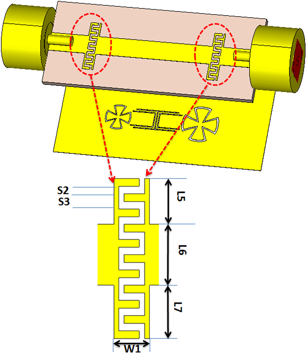
In this section, LPF to BPF transformation is discussed using an interdigital capacitor as a coupling element instead of using a gap J-inverter [Reference Boutejdar, Abd Ellatif, Ibrahim and Challal1]. The configuration of the proposed with an optimized dimension of the BPF is shown in Fig. 6. The coupling element is used to suppress the lower- and upper-frequency bands of the signal. The same previous substrate is used in the design. The capacitance of the interdigital capacitor is calculated as [Reference Hong21]

where, CL, LC, and n are the capacitance, length, and the number of fingers of the interdigital capacitor.
DGS narrow bands BPF configuration with S 3 = 0.3 mm, S 4 = 0.6 mm, L 5 = 1.8 mm, L 6 = 2.4 mm, L 7 = 2.1 mm, and W 1 = 1.4 mm.

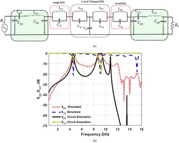
The value of the capacitance of the interdigital capacitor can be controlled using its dimensions. So, the center frequency of the dual bands can be controlled by changing its dimensions. The interdigital capacitor can be modeled using the π section as illustrated in Fig. 7 [Reference Mostafa, Zarezadeh and Ghayoumi-Zadeh22]. The equivalent circuit model of the proposed BPF is illustrated in Fig. 7(a) and the EM simulation in comparison with the circuit simulation is illustrated in Fig. 7(b). It is noticed that the filter is operated in two frequency bands with a center frequency of 4.5 and 9 GHz. The S 21 levels equal 2.1 and 2.2 dB, respectively. The stopband levels between the two bands are lower than −15 dB. The filter has a stopband lower than −15 dB from 10 up to 16 GHz. Also, a good trend is achieved between the two simulators.
DGS narrow bands BPF equivalent circuit analysis. (a) Equivalent circuit model with LS 1 = 0.41 nH, CS 1 = 0.315 pF, LS 2 = 0.35 nH, CS 2 = 0.42pF, LS 3 = 0.66 nH, CS 3 = 0.147 pF, LS 4 = 0.186 nH, CS 4 = 0.418 pF, CP = 0.316 pF, CC 1 = CC 2 = 0.34 pF, LC 1 = 1.45 nH, LC 2 = 1.54 nH, CP 1 = 1.39 nH, and CP 2 = CP 3 = CP 4 = 0.939 pF. (b) S-parameter responses of the EM simulation and circuit simulation.

The proposed BPF is fabricated and tested, and its fabricated photograph is illustrated in Fig. 8. It is seen from the measured results that the filter is BPF with dual and narrow frequency bands operated at a center frequency of 4.5 and 9 GHz, respectively. The S 21 levels of the passbands equal 2.2 dB in both the bands. The stopband levels between the two bands are lower than −13 dB. The filter has a stopband lower than −15 dB from 10 up to 16 GHz. Also, good matching is obtained between the simulated and tested outcomes as illustrated in Fig. 9.
Top and back views of the DGS BPF fabricated prototype.

S-parameters of the simulated and tested results of the proposed DGS BPF.

Proposed wide-band DGS BPF
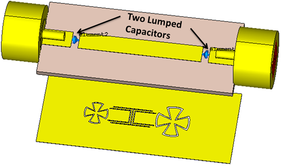
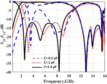
To achieve wideband operation, enhance the filter response, and achieve compact size, lumped capacitors are used as coupling elements between the input/output ports as illustrated in Fig. 10. The lumped capacitors are used to suppress the lower band frequency. The lower band suppression is controlled by changing the lumped capacitor capacitance as shown in Fig. 11. From Fig. 11 it is clear that by increasing the capacitance of the lumped capacitor from 0.5, 1 , and 1.5 pF, the lower-frequency band can be shifted down from 3.5 to 2 and 1.5 GHz respectively. Also, the passband and reflection coefficient responses are enhanced by increasing the capacitance values. The capacitance of 1 pF is used in the fabrication.
DGS wide-band BPF configuration with lumped capacitors.

S-parameter responses of DGS wide-band BPF configuration with different values of lumped capacitors.

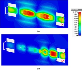
The equivalent circuit model of the proposed BPF is illustrated in Fig. 12(a) and the EM simulation in comparison with the circuit simulation is illustrated in Fig. 12(b). It is noticed that the filter has a wide band operation with a bandpass feature extended from 2 up to 10.6 GHz. The S 21 levels of the passband equal 0.5 dB. The filter has a stopband lower than −15 dB from 11 up to 16 GHz. Also, a good trend is achieved between the two simulators. The electric field distribution of the proposed filter at 8 and 14 GHz inside the substrate is illustrated in Fig. 13. At 8 GHz (passband) the electric field is transferred from port 1 to port 2 while at 14 GHz (stopband) the electric field did not reach port 2.
DGS wide-band BPF equivalent circuit analysis. (a) Equivalent circuit model with LS 1 = 0.41 nH, CS 1 = 0.315 pF, LS 2 = 0.35 nH, CS 2 = 0.42 pF, LS 3 = 0.66 nH, CS 3 = 0.147 pF, LS 4 = 0.186 nH, CS 4 = 0.418 pF, CP = 0.316 pF, and CC = 1 pF. (b) S-parameter responses of the EM simulation and circuit simulation.

Distribution of the electric field inside the substrate at port 1 of the DGS wide-band BPF: (a) at 8 GHz and (b) at 14 GHz.

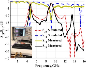
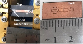
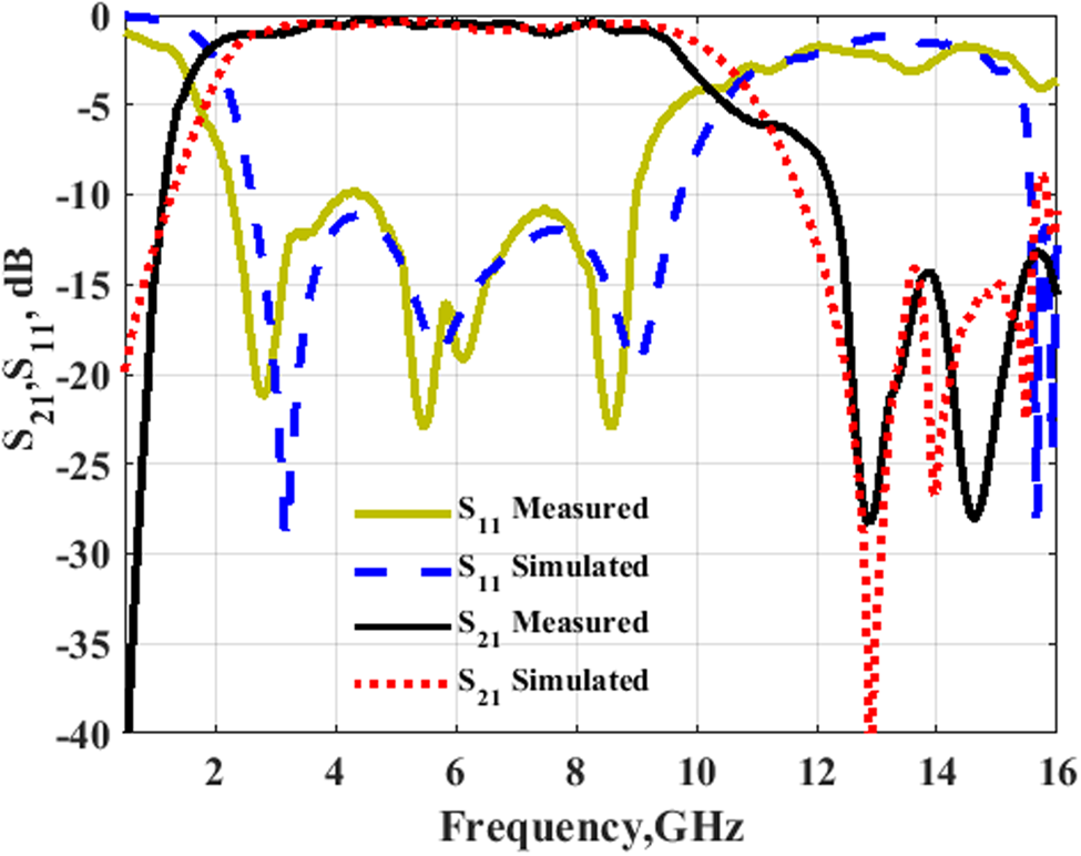
The proposed BPF is fabricated and tested, and its fabricated photograph is illustrated in Fig. 14. It is obvious from the tested results that the filter has a wideband operation with a passband starting from 1.9 up to 10 GHz as illustrated in Fig. 15. The S 21 levels of the passband equal 0.8 dB. The filter has a stopband lower than −15 dB from 10 up to 16 GHz. Also, good matching is obtained between the simulated and tested outcomes. However, a small shift is noticed especially at the upper-frequency band due to the reasons mentioned above in the “LPF” Section. Finally, it is concluded that BPF responses are achieved by using LPF responses without changing the filter size.
Top and back views of the DGS wideband BPF fabricated prototype.

S-parameters of the simulated and tested results of the proposed wideband DGS BPF.

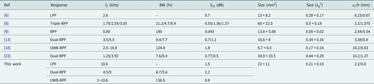
Table 1 compares the suggested filters with the others. The suggested filters have a compact size with high performance which makes it to be a good choice for small-size wireless applications.
Comparison between reported filters and our work

Conclusion
In this paper, three compact LPF/dual-BPF/UWB-BPF of a size of 22 × 11 × 0.8 mm3 have been designed, fabricated, and then measured to validate their simulated outcomes. LPF behavior (0–10 GHz) has been achieved after etching three DGSs from the ground plane. Furthermore, a pair of interdigital and lumped capacitors has been utilized to achieve the dual-band (4.5 and 9 GHz) and the extended UWB (1.9–10 GHz) operations, respectively. The obtained results have verified that the suggested filters have advantages in insertion loss, selectivity, and wide stopband which are very attractive features in modern wireless systems.
Data
There are no supplementary materials, and the data are available upon reasonable request.
Author contributions
All authors contributed equally to analyzing data and reaching conclusions, and in writing of this paper.
Financial support
No funds, grants, or other support were received to conduct this study.
Conflict of interest
The authors report no conflict of interest.
 Hesham A. Mohamed received his B.Sc. in electronics and communication engineering from the University of Menofia in 2003 and his M.Sc. and Ph.D. from Ain Shams University in 2009 and 2014, respectively. He is currently an associate professor at Electronics Research Institute (ERI), Giza, Egypt. Dr. Hesham has teaching experience (more than 12 years) as lecturer in Electronic and Communication Engineering Department in Faculty of Engineering Misr University for Science and Technology. Dr. Hesham is an SMIEEE senior member of the IEEE (Institute of Electrical and Electronic Engineers). He has authored or co-authored nearly 30 journal papers, about 17 refereed conference papers, and has attended and chaired several national and international conferences. He has supervised and co-supervised four Ph.D. and four M.Sc. theses at the Cairo University, Ain Shams University, Benha University, and Helwan University. His outstanding works have been published in international journals and conferences. He is a reviewer of the following international journals: IEEE Microwave and Wireless Components Letters, IEEE Access, Progress in Electromagnetics Research (PIER, PIER B, C, M, PIER Letters), Microwave and Optical Technology Letters, and International Journal of Circuit Theory and Applications. Dr. Hesham participates in more than six research projects at the national and international levels such as Egypt-NSF-USA joint fund program, Egypt STDF-France IRD joint fund program, and the European Committee programs of FP6 and FP7. His role in the following projects is from C-PI to PI: as an RF-design engineer (antenna and power amplifier module) (2018–2020) in the project “Small SAR satellite antenna and transceiver system,” a communication subsystem engineer (2019–2020) in the project “Egyptian University Satellite (EUS-2),” an RF-design engineer (2018–2019) in the project “Design of Radar Absorbing Materials (RAM) using Meta-materials,” a wireless system engineer (2015–2018) in the project “Development of High Data Rate X-Band Transmitter for LEO Remote Sensing Satellites,” an RF-design engineer (2015–2018) in the project “The Egyption 2D Radar,” an RF-design engineer (2011–2014) in the project “Ultra-wideband Ground Penetrating Radar for Water Detection in Egypt,” and an RF-design engineer (February 2011–February 2014) in the project “Novel Planar Antennas for the Most Recent Telecommunications Applications.” His research interests include microwave circuit designs, planar antenna systems, recently on EBG structures, UWB components and antenna and RFID systems, radar absorbing materials, energy harvesting and wireless power transfer, smart antennas, microstrip antennas, microwave filters, metamaterials, and MIMO antennas and its applications in wireless communications.
 Wael A. E. Ali was born in 1982. He received his B.Sc. and M.Sc. in electronics and communications engineering from Arab Academy for Science, Technology and Maritime Transport (AASTMT), Alexandria, Egypt in 2004 and 2007, respectively. He obtained his Ph.D. in electronics and communications engineering from Alexandria University, Alexandria, Egypt in 2012. He is currently a professor at Arab Academy for Science, Technology and Maritime Transport (AASTMT), Alexandria, Egypt. He has published more than 82 peer-reviewed journal and conference papers. His research interests include smart antennas, microstrip antennas, microwave filters, metamaterials, millimetric-wave antennas, and MIMO antennas for various wireless communications applications.
 Ahmed A. Ibrahim (M’19–SM'20) was born in 1986. He received the B.Sc., M.Sc., and Ph.D. in electrical engineering from the Electronic and Communication Engineering Department, Minia University, El-Mina, Egypt in 2007, 2011, and 2014, respectively. He is now an associated professor in the Electrical Engineering Department in the Faculty of Engineering, Minia University. He has been a visiting professor at University Pierre and Marie Curie, Sorbonne University, Paris VI, France for 7 months and Otto-von-Guericke-Universität Magdeburg-Germany for 6 months. He has published more than 95 peer-reviewed journal and conference papers. His research has focused on miniaturized multiband antennas/wideband, microwave/millimeter components, DRA metamaterial antennas, graphene antennas, and microwave filters. Also, his research includes MIMO antennas and energy harvesting systems. Dr. Ahmed A. Ibrahim is a senior member of the IEEE and a senior member in URSI and also a member of the national committee of radio science in Egypt. He is currently a reviewer of IEEE Antennas and Wireless Propagation Letters, IEEE Microwave Wireless Components, IEEE Access, IET Microwave, Antenna and Propagation, IET Electronics Letters, MOTL, Analog Integrated Circuits, and Signal Processing, and many other journals and conferences. In 2020 and 2021, he was named in the top 2% of scientists in “A standardized citation metrics author database annotated for scientific field/Updated science-wide author databases of standardized citation indicators.”