I. INTRODUCTION
We hypothesize that manipulated transport properties can be obtained from variably spaced superlattice (VSSL) structures through band engineering of superlattice materials that leads to enhancement of thermoelectric properties. This presumption is based on electrical studies of VSSL structures by other researchersReference O’Dwyer, Lewis, Zhang and Humphrey1–Reference Humphrey and Linke3and our own investigation into the thermoelectric performance of regular superlattice structures.Reference Bulusu and Walker4, Reference Bulusu and Walker5 This research will demonstrate how variably spaced semiconductor superlattice materials not only outperform equally spaced superlattices but also exhibit anisotropic filtering behavior resulting in directionality of thermoelectric properties. This study is unique because (i) a directional Seebeck coefficient along a single crystalline axis has never been investigated or even suggested, and (ii) VSSLs have not been investigated extensively for thermoelectric applications.
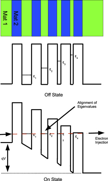
There are two distinct advantages to the electrical and thermal transport properties that arise from controlling the relative film thicknesses within the superlattice structure. The first advantage of increased electrical conductivity is illustrated in Fig. 1 and is a result of electronic confinement of the low lying energy levels of the conduction band within the well region. The second advantage is the reduced thermal conductivity, which is a result of the increased thermal boundary scattering that arises from the varying layer thicknesses of the well regions and the increased number of interfaces. The device geometry of VSSL structures are set by obtaining a favorable electrical structure and assuming the thermal properties will follow. Therefore, no optimization on the structure for coupled electrical/thermal behavior was performed. However, a random configuration was not studied; rather, a structure whose electronic transport follows that of an ideal ballistic device was selected for this study. Discussion of theoretical optimization is not addressed explicitly. Instead the device considered by Humphrey and LinkeReference Humphrey and Linke3 was used as the basis for our coupled thermal/electrical analysis.
Sketch of the VSSL device in the off-state and on-state where there is band alignment and injection of electrons across the structure.

The band structure of the VSSL material can be described by a rectangular periodic potential, where the two different alternating film materials define well and barrier regions with the added complexity of decreasing the well thickness over consecutive well regions. By adjusting the film thickness of the well region, the low lying energy states within this region can be shifted. If the consecutive layer thicknesses are selected appropriately such that they are proportional to the voltage drop, an injection of electrons can be achieved as a result of the apparent alignment of energy levels as in Fig. 1. The directionality of the material arises from the alignment of states when the voltage drop is in the favorable direction, as opposed to a divergence of energy states in the opposing biased direction. For the enhanced transport to occur, the geometry must be tuned for a specific voltage and temperature bias.
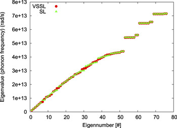
The decreased thermal conductivity of VSSL arises from the phonon spectral response of the structure. Treating each layer of the superlattice structure independently and calculating the frequency content associated with each independent layer provides an argument for a decreased thermal conductivity. The frequency content of the phonons will be a function of the thickness of each individual layer. Therefore, the dispersion, which will be a composite of the frequency content of the individual layers, reveals phononic band gaps or frequencies where phonons are not allowed. Figure 2 shows the eigenvalues of the dynamical matrix, which comprise the dispersion of the superlattice system. The gaps appear whether the device is a VSSL or a regular superlattice. From a particle point of view, a phonon must scatter into an allowed energy state of its neighbor to transport across an interface or tunnel through the neighboring layer to transport energy through the structure. The act of the phonon changing energy at these interfaces results in increased interface scattering, which reduces the thermal conductivity.
Phonon dispersion plot in extended (Brillouin) zone scheme calculated from the harmonic potential assembled. Energy gaps in dispersion are associated with two different masses within each layer of the superlattice.

The argument of phononic band gaps can also be framed in terms of a basis set. Treating the cumulative mass within each independent layer as two different nearest neighbor masses, we can make the analogy that a single bilayer forms a basis set as would be seen in a diatomic crystal. The acoustical branch of the dispersion will depend on the number of atoms within the larger of the two layers. The optical branch will be offset by some energy associated with the smaller of the two masses and form a phononic band gap relative to the top of the previous branch. The number of branches will depend on the total number of bilayers within the structure. The dispersion relation can be conceptualized from the notion of the masses oscillating independently within their associated layer and together across multiple layers. It is the essence of two differing masses periodically arranged within a system that will provide the phononic band gap. Figure 2 is a plot of the phonon dispersion calculated from the harmonic potential used in the phonon nonequilibrium Green’s function (NEGF) formalism. The edge of the Brillouin zone depends on the definition of the basis. Regardless of the definition, the gaps represent the frequency difference between acoustic and optical modes.
A dimensionless figure of merit ZT,
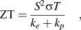
defines the performance of the thermoelectric material, where T is the average temperature, S is the Seebeck coefficient, σ is the electrical conductivity, ke is the electrical contribution to thermal conductivity, and kp is the lattice contribution to thermal conductivity. In the following study we are interested in deriving each quantity within the figure of merit from as close to their inherent physical properties as possible, resulting in a truly quantum calculation without need for quantum correction factors as would be required for a Blotzmann analysis.
Recently, researchers have used the NEGF to calculate both the ballistic electrical and thermal properties independently of similar but less complicated nanostructured materials. Bulusu and WalkerReference Bulusu and Walker4, Reference Bulusu and Walker5 demonstrated the use of NEGFs to look at the thermoelectric performance of strained silicon–germanium superlattices. They showed that for equally spaced superlattice structures that the tunneling can be accurately captured using a one-dimensional (1-D) effective mass Hamiltonian description. They simulated the directions of transport in the cross-plane direction and the remaining two spatial direction were assumed infinite. Bulusu and Walker also demonstrated a quantum confinement effect as a result of the small-layer thickness in the cross-plane direction of the superlattice structures.
Zhang et al.Reference Zhang, Fisher and Mingo6 and Hopkins et al.Reference Hopkins, Norris, Tsegaye and Ghosh7 independently studied the thermal conductivity of cross-plane silicon–germanium superlattices using a phonon NEGF method. Both demonstrated good comparison to available literature and Boltzmann type models.Reference Murphy-Armando and Fahy8 They noted an increased thermal boundary scattering as a result of the interface scattering. Zhang et al. also noted a tapering off of resistivity after 4-5 bilayer construction.
The following research will implement a similar formalism to these two solutions but will combine the independently calculated thermal and electrical transport values from both solutions to determine an overall figure of merit. This approach of combining both solutions has never been carried out for determining the overall figure of merit (ZT) of nanostructured materials.
The electrical and thermal solutions are ballistic in nature and are independent solutions. As a result of the solution being derived independently, there is no thermalizing of electrons or specified mean free path. Both solutions are allowed to reach an independent equilibrium. The effective mean free path is governed by the layer thicknesses of individual layers. Interference scattering or boundary scattering is captured however in both solutions, and we assume that it dominates the conduction of both electrons and phonons in these devices. As a result of the scattering at the boundaries in both simulations, a broadening or distribution of particles form at the contact at discrete energy levels. This broadening is a result of the exclusion principal and provides a meaningful method of connecting infinite contacts to a discrete system, where the particles in the contacts spill over into the channel of the device.
Recent articlesReference Liu, Hoffman, Escarra, Franz, Khurgin, Dikmelik, Wang, Fan and Gmachl9, Reference Bai, Slivken, Kuboya, Darvish and Razeghi10 have applied the same theory of variable superlattice structures to produce monoenergetic lasers with efficiencies up to 50%. BaiReference Bai, Slivken, Kuboya, Darvish and Razeghi10 explains that by aligning the bands between quantum cascading laser (QCL) stages, a high efficiency could be obtained that focuses on the transition between the minibands within the QCL, eliminating phonon production between QCLs. In addition, Bai determined that a thermoelectric effect was apparent in the QCL devices.Reference Escarra, Benz, Bhatt, Hoffman, Wang, Fan and Gmachl11 However, an investigation of these devices for thermoelectric properties was not conducted.
As this concept evolves into experimental studies, the feasibility and limitation of current thin film deposition techniques allow superlattice thicknesses to be controlled on the monolayer scale,Reference Evans, Yu, David, Doris, Mi, Slivken and Razeghi12 providing an avenue for all devices discussed in this study. Many of the fabrication techniques used to construct these devices would follow in the same manner as QCL fabrication.Reference Evans, Yu, David, Doris, Mi, Slivken and Razeghi12 In selecting a material with a similar composition such as Si/Ge, many of the issues related to the crystalline nature can be handled with relative ease. As for other materials with dissimilar crystalline structures, straining and lattice mismatch is much more of a issue at the material interface. For the experimental construction of VSSLs, deposition rate and exposures times would have to be calibrated and varied accordingly, but this is not beyond the capabilities of the current state of fabrication. It is interesting that the construction of superlattice materials proves to be less involved than many of the nanostructured materials currently being experimentally investigated.
The application of VSSLs is not limited to Si/Ge technology but can be applied to other materials and tuned based on their associated band structure. For this study Si and Ge were the materials of choice because of their well-characterized transport thermally and electronically. In addition, an effective mass Hamiltonian can be used to characterize the conduction band edge of both Si and Ge with reasonable confidence. There is also simplification of the thermal analysis by selecting a single compound material because of the isotropic bonding nature. By implementing a material such as degenerate oxides, which may have superior thermoelectric performance compared to our system, the electrical conductivity could be increased dramatically while still maintaining the low thermal conductivity of oxides.
A key aspect that must be taken into account when constructing these materials is the associated strain between layers. For the forthcoming analysis, the strain is treated through an empirical model that relates the conduction band offset to the layer thicknesses of neighboring layers. As the layer thickness changes across the device, the magnitude of the conduction band offset also changes. In comparison to experimental devices, we are studying a relaxed lattice configuration that may require an annealing step during fabrication.
The models used in the research to calculate both the electrical and phonon transport are independent, and no attempt was made to couple the effects of either. These models have been shown independently to provide accurate analysis of Si/Ge nanomaterials. By maintaining a layer thickness below 5 nm, it is assumed that the majority of the transport is ballistic and scattering only occurs at the boundaries of the layers and contacts. The majority of the errors associated with this analysis lie in selecting an effective mass and appropriate harmonic potential constants. With the values selected in this research the ability to reproduce experimental electronic and phonon dispersion gives confidence to our approach and our parameterization.
II. DISCUSSION
A. NEGF ballistic electron model
A Schrödinger–Poisson self-consistent solver was used to calculate the ballistic electronic transport. A NEGF quantum formalism was implemented to capture the quantum effects in a wave-based model as opposed to a particle-based model to calculate the probabilistic nature of electrons without need for quantum correction. The main objective of the NEGF is to obtain the transmission probability between two contacts for a range of energies to implement the Landauer formalism,

which states that the total current is proportional to the quantum conductance (2e 2/h), times the transmission probability (Ξ), times the difference in Fermi energy (f 2 − f 1), integrated over the energy. The current voltage (IV) characteristics of each device are determined from this relation.
One advantage that NEGF provides is the ability to include boundary effects in the model. The contacts are assumed ohmic in nature and are infinite in extent. Broadening at the contacts is a result of the large number of states within the contacts spilling into the device. The broadening of energy levels at the contacts will work to our advantage as the incoming electrons spread near the peak injection energy, loosening the need for the energy levels to be precisely aligned within well regions.
In this treatment of electron transport, an effective mass Hamiltonian is used to describe the dynamics of the electrons. The 1-D Hamiltonian and corresponding eigenvalue problem take the following form:

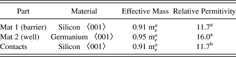
Because the transport is only along a single crystal axis and the remaining two spatial direction are infinite, a 1-D solution is satisfactory for determining the ballistic transport. Because electron–phonon scattering is not included, the transverse momentum is integrated out of the Hamiltonian relation.Reference Datta13Table 1 outlines a few of the material parameters used in the model.
Electronic NEGF material parameters.
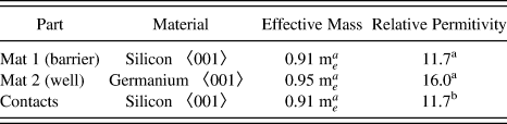
a Bulusu and Walker.4
b Kittel.16
The boundaries at either contact are assumed infinite in extent and described by a 〈001〉 silicon effective mass. The superlattice series begins with a confined layer of strained 〈001〉 silicon. The next adjacent layer in the series is strained 〈001〉 germanium. The alternating series of layers continues and ends with an infinite contact as at the beginning. The straining of both layers is important in capturing an accurate description of the band structure. Straining was applied through a band offset description parameterized by the weighted average thickness of neighboring layers and an associated deformation potential for each material. The theory of straining is outlined by Van de WalleReference Van de Walle14 along with associated deformation potentials for Si/Ge. It is important to point out that the conduction band edge of unstrained siliconReference Krishnamurthy, Sher and Chen15 along 〈001〉 is greater in energy than that of 〈001〉 germanium. However, under the presence of straining the conduction band edge undergoes an inflection in which the silicon become a minimum. This is important to the transport because we are interested in modifying the low lying states within the well region.
The conduction band edges are referenced from a constant Fermi energy of 0.1 eV. By initially specifying the temperature at either contact, the system begins at a nonequilibrium state. The Fermi functions at either contact are specified with a temperature difference, which imposes nonequilibrium on the system. By opposing the temperature induced current with a voltage, the equilibrium condition can be achieved.
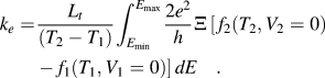
The electronic thermoelectric parameters are calculated by initially specifying a temperature difference between the two contacts. A resulting current is calculated using Eq. (2) for electron energy from −0.4 to 1 eV spanning the lowest conduction levels and  above the highest barrier. The calculation begins by determining the electrical current at zero voltage bias with a specified temperature bias defining the electrical contribution of the thermal conductivity. Next, a voltage in the opposite direction of the temperature bias is incrementally increased until the current across the system becomes zero, defining the Seebeck voltage of the structure. In addition, the electrical conductivity is determined by calculating the slope of the IV curve near the Seebeck voltage using a forward difference.
The thermal conductivity due to the electron contribution is calculated from the zero bias nonequilibrium state, where the current across the system is driven by the specified temperature difference at the contact [see Eq. (4)]. It is well accepted that the Wiedemann–Franz law loses validity in nanostructures; therefore, the thermal conductivity due to the electron contribution is calculated in this manner and the lattice contribution is calculated using a phonon NEGF method. Because the phonon NEGF solution is independent, there is no thermalizing of electrons and the lattice thermal conductivity is only derived from the phonon NEGF solution.
B. NEGF ballistic phonon model
An atomistic NEGF method is applied in a similar manner to the electronic NEGF to calculate the thermal transport. Added complexity in the description of the Hamiltonian stems from a discretization scheme in which the cell center corresponds to equilibrium atom positions. Conversely, the phonon solution does not require self-consistency with an external field, decreasing the computational time required to reach a solution. The NEGF phonon treatment is a wave-based solution, and we treat phonons as waves not particles, accounting for the tunneling of phonons similar to electrons. Using a similar expression to the Landauer formalism, we can calculate the total thermal energy (q tot) transported as a function of the integrated transmission probability and single phonon mode (ℏω).

Applying Fourier’s law and the known temperature gradient between contacts, the phonon thermal conductivity (kp) can be calculated.
A 1-D chain of atoms with the same boundary constraints as specified for the electrical NEGF is applied to the phonon domain. A Hamiltonian description is written based on an atomistic harmonic potential. The Hamiltonian takes the following form:
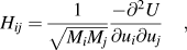
where Mi and Mj are the neighboring masses and ui and uj are the displacements. The U parameter is the potential energy determined by the interatomic pair potential. The finite difference scheme used to approximate the derivate must construct a Hermitian space as was required in the electronic Hamiltonian.
The atomistic harmonic potential is described by an interatomic pair potential derived from the equilibrium position of atoms and the lattice position of atom planes within the device. The harmonic matrix is constructed using the Harrison potentialReference Harrison17 that derives the potential energy of the system from the individual bonding energy of nearest neighbors and the displacement of the atoms from their equilibrium position:
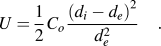
The material parameters used in the phonon NEGF model are outlined in Table II.

For this study we selected the harmonic Harrison potential because it has been used successfully by others.Reference Zhang, Fisher and Mingo6, Reference Hopkins, Norris, Tsegaye and Ghosh7 Additional pair potentials and three body potentials, are applicable, but the Harrison potential was adequate for reproducing the experimental phonon dispersion. Because we are calculating the 1-D transport assuming the two other directions are periodic, the oscillatory behavior can be conceptualized as planes of atoms oscillating normal to each other along the 〈001〉 direction. The behavior of planes oscillating in the direction of transport constrains our model to capturing only the longitudinal phonon modes within the structure.
III. RESULTS AND DISCUSSION
In this study the performance of the VSSL is investigated as a function of temperature for three different material configurations. The two VSSL materials of interest have a total length of approximately 55 nm and comprise seven silicon and germanium layers with a silicon cap, forming seven heterojunctions not including the two contact junctions. The dopant concentration is maintained at 1018 cm−3 and the temperature difference across the device is constant at 10 K. The hot contact (305 K) is the right contact, and the cold contact (295 K) is the left contact.
The selection of the material configuration was based on demonstrating the trends associated with a VSSL and a non-VSSL material. There was no attempt to optimize the VSSL structure in this research but rather to show a performance difference. Because of the distribution of electrons entering the system, the strict energy level alignment of consecutive layers is relaxed. However, perfect alignment of the energy levels is optimal, but using an approximate structure is reasonable for proof of concept. To design a general VSSL structure, the thickness of consecutive layers can be estimated under simple assumptions. Because the Seebeck voltage is dependent on the device geometry, this estimated design is only an approximation. To calculate an approximate structure, first focus on only two neighboring well regions, assuming the voltage drop is linear across the whole device region and the confined energy levels of the well follow the relation

where a is the layer thickness. The neighboring layer has energy levels that follow
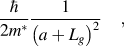
where Lg is an incremental increase or decrease of the neighboring layer thickness. Equating the voltage drop across the entire device region to the voltage drop between the neighboring layers, a relation can be written as follows:
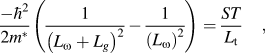
where Lω is the well width, L b is the barrier width, L g is the increment of consecutive layers, and L t is the total length. Specifying a device length of 55 nm and assuming the approximate Seebeck to be 500 μV/K, for a 55-nm device with a 10 K temperature bias the Lg parameter is 0.508 nm, which is the basis for selecting 0.5 nm as the increment for the remaining studies in this research.
In the context of Humphrey and Linke’s3 work, where they were interested in adjusting  , this work is interested in satisfying a similar condition, however, by adjusting the lowest energy levels [E 0(x)] not the spatial doping patterns.
The first material of interest is a +0.5-nm VSSL (+VSSL); the thickness of the well region is increased consecutively by 0.5 nm over seven well regions and the barrier region is maintained at 5 nm. The first well region has a thickness of 0.5 nm, and the last well region in the series has a thickness of 4 nm. The volume fraction of silicon within this material is approximately 51.4% Si. The second material is a -0.5-nm VSSL (−VSSL); the construction is the same as the first material except the bias is applied in the opposite direction. The third material, a non-VSSL structure, has a total length of 60 nm with seven heterojunctions and the individual layers all have a thickness of 4 nm for both the well and barrier regions.
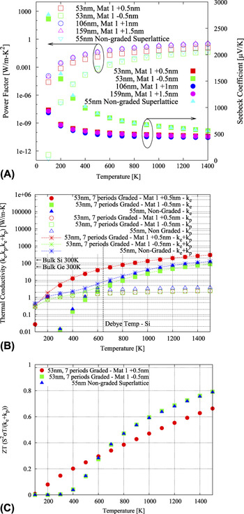
The three structures are simulated at various temperatures to facilitate a relative comparison of performance. Figure 3 includes plots of the power factor (PF), thermal conductivity, and ZT for the three structures as a function of temperature. The first plot demonstrates the PF = S 2σ as a function of temperature labeled with closed symbols associated with the left axis. On the same plot, the Seebeck coefficient S is plotted with open symbols associated with the right axis. The trends of the PF are typical for common thermoelectric materials for increasing temperature. The PF increased for all structures as the temperature increased, and the relative difference in PF between the VSSL and non-VSSL structure decreased with increasing temperature. These trends are a result of the increased electron population as the temperature increases and corresponding to the increased number of tunneling electrons between contacts. Referring to Table II, as the Fermi function of either contact increases with temperature, the current will also increase proportionally, resulting in greater conductivity that ultimately influences the PF.
Ballistic electrical and thermal properties calculated for two oppositely graded VSSL and non-VSSL materials as a function of temperature. Circles: +0.5-nm grading (+VSSL); squares: −0.5-nm grading (−VSSL); triangles: no grading (non-VSSL). The +VSSL material has a ZT of 0.20 compared to a ZT of 0.04 for the non-VSSL at 400 K. Lines were added to guide the eye.

Focusing on the PF at 300 K for the +VSSL (closed circles), a value of approximately  compared to
 for a non-VSSL material is apparent. The PF is greater for the +VSSL material because the electrical conductivity increases considerably because of the alignment of energy levels, resulting in the injection of the electrons across the structure. Investigating the PF of the −VSSL and non-VSSL suggests that the PF values are relatively close to each other as a result of the nonalignment of energy levels. In essence, the nonaligned level cause the transport in the −VSSL structure to be governed by tunneling through barriers and wells as seen in a traditional (uniform) superlattice (non-VSSL) structure.
In the same plot in Fig. 3, focusing on the Seebeck voltage (open symbols), as the temperature increases the Seebeck decreases, contrary to what was depicted for the PF values (closed symbols). Comparing the Seebeck values for the +VSSL structure at 300 K to that of the non-VSSL suggests that the Seebeck coefficient decreases at the expense of a large electrical conductivity. This is a common trend in most materials where the Seebeck coefficient and electrical conductivity are inversely related. The Seebeck increases as a result of the material’s ability to maintain a greater charge distribution as seen in the non-VSSL and −VSSL structures.
Comparing both the +VSSL and −VSSL Seebeck coefficients from the first plot of Fig. 3, an apparent directionality is present. At 300 K the Seebeck voltage is nearly double for the –VSSL compared to the +VSSL. This directionality trend is reversed for the PF values because of the electrical conductivity having the opposite direction trend compared to the Seebeck. The directionally is depicted in both the Seebeck and electrical conductivity, but the PF trends are mostly influenced by the conductivity trends.
The second plot in Fig. 3 is the thermal conductivity as a function of temperature. The electronic contribution ke of the thermal conductivity (open symbols) and the thermal contribution kp of the thermal conductivity (closed symbols) are both plotted. The summation of the electron and phonon contributions are composed into a single thermal conductivity  value depicted by the dashed lines. The total conductivity of the +VSSL material is the red line, the green line is the −VSSL, and the blue line is the non-VSSL in the online color version.
The electrical contribution of the thermal conductivity ke for the +VSSL (solid circles, Fig. 3) has the largest overall conductivity of all the structures. This is a result of the electrons that carry thermal energy experiencing the same increase in conductivity due to alignment of energy levels of the transport electrons. For a majority of the temperature range the +VSSL thermal conductivity is almost entirely influenced by ke from 200 K and higher. For the –VSSL and the non-VSSL material there is a transition at approximately 600 K in the dominate mechanism of thermal conductivity. Prior to this transition temperature the phonon thermal conductivity kp is dominant; however, past 600 K the total thermal conductivity is dominated by the electrical contribution ke. This transition is situated close to the Debye temperature of silicon (645 K) where the phonon conductivity kp plateaus. The Debye temperature of germanium is approximately 374 K and the Debye temperature of the superlattice structure is that of the material with the greater Debye temperature. As the temperature increased above the superlattice, the Debye temperatures of the +VSSL and −VSSL/non-VSSL structure are dominated by both the ke contribution and follow a similar trend.
Using Eq. (1), the ZT can be calculated from the composite of the two previous plots of PF and thermal conductivity. Multiplying the PF times the temperature T and dividing by the total thermal conductivity ke + kp, we arrive at the overall ZT value. The calculated ZT as a function of temperature (third plot, Fig. 3) demonstrates that the +VSSL materials (closed circles) outperform the other two materials up to the thermal conductivity transition temperature of approximately 600 K. This transition temperature, as mentioned before, is a result of the electrical contribution ke of the thermal conductivity dominating the total thermal conductivity. In addition, because of the increasingly large thermal conductivity value, as the temperature increases the denominator of the ZT is overwhelmed by the trends of the thermal conductivity.
At a temperature of 400 K, a ZT of 0.20 for the +VSSL and a ZT of 0.04 for the non-VSSL material were calculated, resulting in a 5 times increase in the ZT for a +VSSL material. These results suggest that +VSSL structures can achieve a greater ZT at room temperature over a non-VSSL because of a 17 times increase in PF and only a 4 times increase in thermal conductivity. The transition region where the non-VSSL begins to outperform the +VSSL material is associated with the electrical contribution ke of the total thermal conductivity dominating the ZT. Again, comparing the +VSSL and −VSSL structure, a directional dependence arises in the ZT plot and is heavily apparent at temperatures below 600 K. In addition, the −VSSL structure follows the trend of the non-VSSL structure as expected because of the lack of alignment, resulting in mainly tunneling electrical transport similar to the non-VSSL structure.
IV. CONCLUSION
This research used two different quantum NEGF models to determine the ballistic transport of both the electrons and phonons for three configurations: two VSSL materials and a non-VSSL material. The NEGF approach allowed the appropriate boundary effects to be captured while maintaining a quantum description of the transport. It was determined that a VSSL designed with increasing well layer thickness in the direction of decreased thermal gradient results in a considerable increase of electrical conductivity arising from the band alignment under closed circuit conditions. A 17 times increase in electrical conductivity is associated with a 5 times greater ZT at room temperatures compared to a non-VSSL. Conversely, a 4 times increase in thermal conductivity results from the increased transport of thermally excited electrons but was outweighed in the ZT by the greater performance increase in the PF. A transition temperature at which the non-VSSL begins to outperforms VSSL materials was captured near the Debye temperature of the material. The directionality of the VSSL was a result of the opposing bias recovering the tunneling transport properties of a non-VSSL structure. These finding support the use of VSSLs to further enhance the thermoelectric performance of nanostructured materials.