I. INTRODUCTION
In 1961, Shockley and QueisserReference Shockley and Queisser1 correlated the maximum theoretical efficiency achievable by a single-junction solar cell to the energy gap E g of the absorbing material. The Shockley–Queisser (SQ) limit moves from the observation that, while the solar spectrum is continuous over a wide range of frequencies, a photovoltaic (PV) cell efficiently converts only photons at the frequency corresponding to the energy gap of its absorbing component. Actually, photons with energy lower than E g are not absorbed while photons with energy larger than E g partially convert their energy into heat, setting the cell temperature (T cell). Several solutions were proposed and implemented to overcome this limit. Among them, the conversion of the unused heat released by solar cells into useful work is becoming increasingly popular. These devices, named hybrid thermo–photovoltaic (HTPV) systems, may adopt a host of ways to recover and convert such thermal energy.Reference Chow2–Reference Wang, Han, He, Park and Koumoto6 In this study, we focus on a specific class of HTPV devices, wherein a thermoelectric generator (TEG) is placed underneath the solar cell. We will refer to such systems as hybrid thermoelectric-photovoltaic (HTEPV) devices. In a previous study,Reference Lorenzi, Acciarri and Narducci7 we showed that the amount of recoverable power in HTEPV devices mainly depends upon two parameters of the absorbing material, namely its energy gap and its working temperature under illumination. The aim of this work is to propose a theoretical model correlating the dependence of the HTEPV device performances upon these parameters. We will consider two possible cases. In the first one, a simple coupling between the PV cell and the thermoelectric part is considered, and the TEG only converts the portion of the solar spectrum with photons energy larger than E g. In the second one, an additional absorbing layer is introduced to convert the subgap part of the solar radiation into heat. In this case, we will find a range of parameter values such that the performance of the hybrid device significantly exceeds that of the PV cell. Even more interestingly, we will show that in the latter case the HTEPV efficiency exceeds that expected in a PV device operating at room temperature.
II. TEMPERATURE DEPENDENCE OF THE SQ LIMIT
As reported in a previous publication,Reference Lorenzi, Acciarri and Narducci7 losses in single-junction solar cell are due to several causes:
(i) Optical losses due to the contact grid shadow, unintended reflections, and spurious absorptions;
(ii) source-absorber decoupling losses due to nonabsorbed photons with E < E g and to thermalization of hot carriers generated by photons with E > E g;
(iii) thermal losses (Joule effect);
(iv) electrical losses due to nonunitary quantum efficiency and material defects;
(v) recombination losses via radiative or nonradiative recombination processes.
The electric power produced by a solar device is known to decrease with its working temperature. This is due to the increase of the electron–hole recombination rate. As a result, a larger dark saturation current is expected when the cell temperature increases, affecting in turn V oc.Reference Gray, Antonio and Steven8 The relationship between V oc and T cell is approximately linear. Since the short-circuit current J sc is instead just marginally affected by the increase of T cell, the output power  $P_{{\rm{PV}}}^{{\rm{out}}}$ is also proportional to
 $\mathop {{T_{{\rm{cell}}}}}\nolimits^{ - 1}$—and so is its efficiency ηPV. This decrease of the PV cell performance was widely confirmed by experimental works.Reference Friesen, Pavanello and Virtuani9–Reference Skoplaki and Palyvos11
The SQ limit neglects optical, thermal, and electrical losses, thus accounting only for losses of type (ii) and (v). Furthermore, it assumes that T cell equals room temperature. In this section, we will rewrite the SQ limit by relaxing such assumption, namely letting T cell be larger than 300 K to evaluate the maximum achievable efficiency for a single-junction PV cell as a function of its actual operating temperature. Such calculation is required to properly model its contribution to the overall efficiency of the hybrid device.
Following Shockley and QueisserReference Shockley and Queisser1 we assume that: (i) the solar cell is oriented normal to the sunlight beam; (ii) all photons with energy larger than the absorber energy gap are absorbed, while photons with smaller energies produce no effect; (iii) the device has unitary quantum efficiency, i.e., any absorbed photon generates an electron–hole pair at a voltage V γ = E γ/q (where E γ is the photon energy and −q is the electron charge); (iv) the only mechanism of electron–hole recombination is radiative.
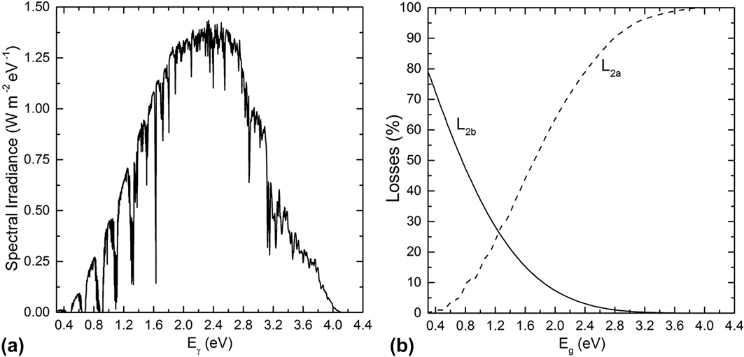
To compute the maximum PV efficiency, we will use the ASTM data for the AM1.5 solar spectrum with an intensity of 1000 W/m2 [Ref. 12, Fig. 1(a)], and cutoff energies E min = 0.30 eV and E max = 4.4 eV. The distribution function of the incident photon flux n γ(E γ) (in eV−1 cm−2 s−1) is then obtained by dividing the spectral intensity by the photon energy. In view of assumptions (i) and (ii), one evaluates the fractions of energy loss due to photons with E < E g
 $${L_{2{\rm{a}}}}\left( {{E_{\rm{g}}}} \right) = {{\int_{{E_{{\rm{min}}}}}^{{E_{\rm{g}}}} {{n_\gamma }\left( {{E_\gamma }} \right){E_\gamma }{\rm{d}}{E_\gamma }} } \over {\int_{{E_{{\rm{min}}}}}^{{E_{{\rm{max}}}}} {{n_\gamma }\left( {{E_\gamma }} \right){E_\gamma }{\rm{d}}{E_\gamma }} }}\quad ,$$
and to photons with E > E g (causing carrier thermal relaxation)
 $${L_{2{\rm{b}}}}\left( {{E_{\rm{g}}}} \right) = {{\int_{{E_{\rm{g}}}}^{{E_{{\rm{max}}}}} {{n_\gamma }\left( {{E_\gamma }} \right)\left( {{E_\gamma } - {E_{\rm{g}}}} \right){\rm{d}}{E_\gamma }} } \over {\int_{{E_{{\rm{min}}}}}^{{E_{{\rm{max}}}}} {{n_\gamma }\left( {{E_\gamma }} \right){E_\gamma }{\rm{d}}{E_\gamma }} }}\quad .$$
(a) AM1.5 solar spectrum used for all calculations reported in this study; (b) energy losses L 2a and L 2b versus the absorber material energy gap.

These quantities are displayed as a function of the energy gap of the absorber material in Fig. 1(b). The overall incoming power per unit area reads instead 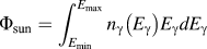 ${\Phi _{{\rm{sun}}}} = \int_{{E_{{\rm{min}}}}}^{{E_{{\rm{max}}}}} {{n_\gamma }\left( {{E_\gamma }} \right){E_\gamma }d{E_\gamma }}$. As previously showed,Reference Lorenzi, Acciarri and Narducci7 the latter PV loss can be connected to T cell by invoking heat current conservation:
 $${L_{2{\rm{b}}}}\left( {{E_{\rm{g}}}} \right){\Phi _{{\rm{sun}}}} = {U_{\rm{L}}}\left( {{T_{{\rm{cell}}}} - {T_{\rm{a}}}} \right)\quad ,$$
where U L is the overall thermal conductance between the cell and the ambient (with temperature T a).
The spectral power above the energy gap
 $${\Phi _{{\rm{above}}}}\left( {{E_{\rm{g}}}} \right) = \int_{{E_{\rm{g}}}}^{{E_{{\rm{max}}}}} {{n_\gamma }\left( {{E_\gamma }} \right){E_\gamma }{\rm{d}}{E_\gamma }} \quad ,$$
contributes on the other hand to carrier generation according to assumption (iii) and sets the current density produced by the device in the absence of radiative recombination. Radiative recombination depends upon the probability of collisional events between holes and electrons, then depending on the difference between hole and electron quasi-fermi levels. Thus, the current density J generated by the solar device can be written as
 $$J = q\left\{ {{N_{\gamma ,{\rm{above}}}}\left( {{E_{\rm{g}}}} \right) - {r_0}\left[ {\exp \left( {{{qV} \over {{k_{\rm{B}}}{T_{{\rm{cell}}}}}}} \right) - 1} \right]} \right\}\quad ,$$
where
 $${N_{\gamma ,{\rm{above}}}}\left( {{E_{\rm{g}}}} \right) = \int_{{E_{\rm{g}}}}^{{E_{\max }}} {{n_\gamma }\left( {{E_\gamma }} \right){\rm{d}}{E_\gamma }} \quad ,$$
k B is the Boltzmann constant, V is the external bias on the junction, and r 0 is the radiative recombination rate when there quasi-fermi energies equal each otherReference Schroder13:
 $${r_0} = {{2\pi } \over {{c^2}{h^3}}}\int_{{E_{\rm{g}}}}^{{E_{{\rm{max}}}}} {{{E_\gamma ^2{\rm{d}}{E_\gamma }} \over {\exp \left[ {{{\left( {{E_\gamma } - qV} \right)} \mathord{\left/ {\vphantom {{\left( {{E_\gamma } - qV} \right)} {{k_{\rm{B}}}{T_{{\rm{cell}}}}}}} \right. \kern-\nulldelimiterspace} {{k_{\rm{B}}}{T_{{\rm{cell}}}}}}} \right]}}} \quad .$$
Using Eq. (5), one can find the maximum power output  $P_{{\rm{PV}}}^{{\rm{out}}}\left( {{E_{\rm{g}}}} \right)$ by maximizing J × V for a given E g. The ratio between
 $P_{{\rm{PV}}}^{{\rm{out}}}\left( {{E_{\rm{g}}}} \right)$ and Φsun returns the cell maximum efficiency, namely the SQ limit, as a function of E g and T cell. Furthermore, J sc and V oc can be obtained from Eq. (5), the former by setting V = 0 and the latter by setting J = 0. This will eventually lead to compute the so–called filling factor FF that is used to write the solar cell efficiency:
 $${\eta _{{\rm{PV}}}} = {{{V_{{\rm{oc}}}}{J_{{\rm{sc}}}}{\rm{FF}}} \over {{\Phi _{{\rm{sun}}}}}}\quad .$$
It may be worth noting that the present calculation (as the original SQ scheme) neglects any temperature profile within the PV cell. Actually, although there is clearly a temperature gradient between the front and the back of the cell, introducing such correction leads to very minor numerical changes in the final result as in all equations T cell always appears within Arrenhius–like terms [e.g., exp(E γ − qV)/k BT cell] but in Eq. (3). Since it is easy to verify that temperature differences up to some tens of kelvins lead to numerical corrections of less than 1% in all Arrhenius terms, we will safely and consistently take T cell as the temperature of the cell back and will keep disregarding temperature gradients moving from the back to the front of the PV cell.
One can now use the explicit dependence on T cell [Eqs. (5) and (7)] to plot the SQ maximum efficiency ηPV(E g, T cell). Figure 2(a) shows ηPV(E g, T cell) for E g and T cell ranging between 0.5 and 2.5 eV and between 300 and 500 K, respectively. The calculation returns that the maximum efficiency at 300 K is ∼33.6% at ∼1.34 eV. This is in good agreement with the literature.Reference Sze14
SQ limit versus temperature. (a) Maximum PV efficiency (%) as a function of E g and T cell. (b) Same as (a) but normalized to the PV efficiency for T cell = 300 K.

For any E g, we observe that ηPV(E g, T cell) decreases when the temperature increases. The decrease is steeper for small gaps. This trend is easily understood considering that for small gaps the probability of radiative recombination is higher and then the maximum efficiency shifts toward higher E g for increasing T cell. This feature is even more evident when plotting the ratio ηPV(E g, T cell)/ηPV(E g, 300 K) [Fig. 2(b)]. Thus, one may conclude that while it is true that the best achievable efficiency occurs for E g around 1.3 eV, the performances deteriorate much faster with the T cell for smaller E g. As we will see, this is actually the key point to evaluate when coupling in HTEPV can be beneficial.
III. HTEPV DEVICE MODELING
As already mentioned, in HTEPV devices a TEG is basically connected thermally and electrically in series to the PV stage. In what follows we will discuss two different device structures. In the first structure (hereafter Case 1), the TEG is just placed underneath the solar cell and is electrically connected to it [Fig. 3(a)]. Therefore, T cell follows from Eq. (3) and the only part of the spectrum that can be recovered by the TEG is L 2b(E g). It should be remarked that, although in principle some of the materials used in the TEG module could also absorb (and convert into heat) photons with energies below the energy gap, one should also consider that the back contact of most solar cells is made of metallic materials (e.g., silver, aluminum, gold, or molybdenum) which are normally highly reflective. Thus, since in Case 1 the solar cell back contact is placed on top of the TEG device, only a negligible portion of L 2a(E g) (not absorbed by the cell) will reach (and will eventually be absorbed) by the TEG component. In this sense, Case 1 may be considered as a conservative model for the real direct coupling of a PV cell and a TEG device.
Schematics of the device structures discussed in this work. (a) Case 1, in which the TEG is just placed underneath the solar cell and is electrically connected to it; (b) C, where also the portion of the spectrum with E γ < E g (L 2a) is recovered by introducing an additional absorbing layer.
On the other hand, in the second construction (Case 2) we recover also the portion of the spectrum with E γ < E g by adding an absorbing layer on top of the solar cell back contact, or by modifying the solar cell back contact so as to make it acting as a black body, capable to convert this part of the spectrum into heat [see Fig. 3(b)]. Therefore, the power fraction recovered by the TEG is L 2a(E g) + L 2b(E g) and Eq. (3) has to be modified as
 $$\left[ {{L_{2{\rm{a}}}}\left( {{E_{\rm{g}}}} \right) + {L_{2{\rm{b}}}}\left( {{E_{\rm{g}}}} \right)} \right]{\Phi _{{\rm{sun}}}} = {U_{\rm{L}}}\left( {{T_{{\rm{cell}}}} - {T_{\rm{a}}}} \right)\quad ,$$
that sets ideal heat dissipation conditions. Thus, the TEG will convert the heat flowing through its thermoelectric elements working between T cell and T a. The output power reads then
 $$P_{{\rm{TEG}}}^{{\rm{out}}} = {\eta _{{\rm{TEG}}}}{L_{2{\rm{b}}}}\left( {{E_{\rm{g}}}} \right){\Phi _{{\rm{sun}}}}\quad ,$$
for Case 1 and
 $$P_{{\rm{TEG}}}^{{\rm{out}}} = {\eta _{{\rm{TEG}}}}\left[ {{L_{2{\rm{a}}}}\left( {{E_{\rm{g}}}} \right) + {L_{2{\rm{b}}}}\left( {{E_{\rm{g}}}} \right)} \right]{\Phi _{{\rm{sun}}}}\quad ,$$
for Case 2.
In both equations ηTEG is given by
 $${\eta _{{\rm{TEG}}}} = \left( {1 - {{{T_{\rm{a}}}} \over {{T_{{\rm{cell}}}}}}} \right){{\sqrt {1 + Z\bar T} - 1} \over {\sqrt {1 + Z\bar T} + {{{T_{\rm{a}}}} \mathord{\left/ {\vphantom {{{T_{\rm{a}}}} {{T_{{\rm{cell}}}}}}} \right. \kern-\nulldelimiterspace} {{T_{{\rm{cell}}}}}}}}\quad ,$$
where ZT is the thermoelectric figure of merit and  $\bar T = {{\left( {T_{{\rm{cell}}} + T_{\rm{a}} } \right)} \mathord{\left/ {\vphantom {{\left( {T_{{\rm{cell}}} + T_{\rm{a}} } \right)} 2}} \right. \kern-\nulldelimiterspace} 2}$. Thus,
 $$\eta _{{\rm{TEG}}}^{{\rm{out}}} = {{P_{{\rm{TEG}}}^{{\rm{out}}}} \over {{\Phi _{{\rm{sun}}}}}} = \left\{ \matrix{ {\eta _{{\rm{TEG}}}}{L_{2{\rm{b}}}}\left( {{E_{\rm{g}}}} \right)\,\,\,\,\,\,\,\,\,\,\,\,\,\,\,\,\,\,\,\,\,\,\,\,\,\,\,\,\,\,\,\,\,\,{\rm{CASE}}\;1 \hfill \cr {\eta _{{\rm{TEG}}}}\left[ {{L_{2{\rm{a}}}}\left( {{E_{\rm{g}}}} \right) + {L_{2{\rm{b}}}}\left( {{E_{\rm{g}}}} \right)} \right]\,\,\,{\rm{CASE}}\;2 \hfill \cr} \right.\quad ,$$
and the hybrid device efficiency reads
 $${\eta _{{\rm{HTEPV}}}} = {{P_{{\rm{PV}}}^{{\rm{out}}} + P_{{\rm{TEG}}}^{{\rm{out}}}} \over {{\Phi _{{\rm{sun}}}}}} = \left\{ \matrix{ {\eta _{{\rm{PV}}}} + {\eta _{{\rm{TEG}}}}{L_{2{\rm{b}}}}\left( {{E_{\rm{g}}}} \right)\,\,\,\,\,\,\,\,\,\,\,\,\,\,\,\,\,\,\,\,\,\,\,\,\,\,\,\,\,\,\,\,\,\,\,{\rm{CASE}}\;1 \hfill \cr {\eta _{{\rm{PV}}}} + {\eta _{{\rm{TEG}}}}\left[ {{L_{2{\rm{a}}}}\left( {{E_{\rm{g}}}} \right) + {L_{2{\rm{b}}}}\left( {{E_{\rm{g}}}} \right)} \right]\,\,\,\,{\rm{CASE}}\;2 \hfill \cr} \right.\quad .$$
The previous equations assume that the addition of the TEG stage will not impact on the solar cell efficiency. However, this hybridization will surely change the bias voltage of the PV section. Lossless PV–TEG hybridization was however demonstrated to be possible.Reference Park, Shin, Tazebay, Urn, Jung, Jee, Oh, Park, Yoo, Yu and Lee5 This legitimates that calculations be carried out assuming that the initial PV efficiency could be kept unchanged by properly adjusting the electrical resistance of the TEG section.
IV. RESULTS AND DISCUSSIONS
In what follows all results are computed considering TEG material pairs having ZT = 1 constant over the TEG thickness. Since only small temperature differences are considered, this assumption is acceptable and adequate for most thermoelectric materials of practical interest.Reference Cao, Zhao, Zhu, Zhang and Tu15–Reference Yan, Poudel, Ma, Liu, Joshi, Wang, Lan, Wang, Chen and Ren17
A. Direct coupling (Case 1)
The case of no extra absorbing layer HTEPV is reported in Fig. 4. Figure 4(a) shows the TEG output efficiency as a function of E g and T cell. In this configuration, the TEG only converts the portion of the spectrum above the gap of the absorber. Thus,  $\eta _{{\rm{TEG}}}^{{\rm{out}}}$ increases for decreasing E g. On the other hand, and manifestly enough, for any given E g we observe
 $\eta _{{\rm{TEG}}}^{{\rm{out}}}$ to increase with T cell.
HTEPV efficiency: Case 1. (a) TEG efficiency (%) versus E g and T cell. (b) HTEPV efficiency (%) versus E g and T cell, normalized to the PV efficiency for T cell = 300 K.
Figure 4(b) shows the HTEPV efficiency normalized to ηPV at 300 K. It shows that the most important effect of the TEG stage is to mitigate the decrease of ηPV with increasing T cell. This effect is more evident for small E g, that is, when the TEG contribution to the total efficiency is larger. Therefore, the HTEPV device performs better than the PV alone, especially for small energy gaps. However, considering the range of temperatures normally reached by a solar cell under illumination (320–350 K)Reference Nordmann and Clavadetscher10, the advantage seems unlikely to justify the effort needed to add the TEG stage.
B. Use of an intermediate absorbing layer (Case 2)
In the presence of an extra absorbing layer able to covert the subgap fraction (L 2a) of the solar spectrum, the cell temperature is set by both L 2a and L 2b. Figure 5(a) shows the TEG output efficiency as a function of E g and T cell. In this case for small T cell,  $\eta _{{\rm{TEG}}}^{{\rm{out}}}$ stays nearly constant for any E g, with a shallow minimum around 1.25 eV at high temperatures. The difference between minimum and maximum
 $\eta _{{\rm{TEG}}}^{{\rm{out}}}$ values increases by increasing T cell.
HTEPV efficiency: Case 2. (a) TEG efficiency (%) versus E g and T cell. (b) HTEPV efficiency (%) versus E g and T cell, normalized to the PV efficiency for T cell = 300 K.
Figure 5(b) shows the HTEPV efficiency normalized to ηPV at 300 K. While for small E g the situation is similar to that seen in Fig. 4(b), new interesting features show up for intermediate and wide energy gaps. In fact in this region,  ${{\eta _{{\rm{TEG}}}^{{\rm{out}}}} \mathord{\left{\vphantom {{\eta _{{\rm{TEG}}}^{{\rm{out}}}} {{\eta _{{\rm{PV}}}}\left( {{E_{\rm{g}}},\;300\;{\rm{K}}} \right)}}} \right\kern-\nulldelimiterspace} {{\eta _{{\rm{PV}}}}\left( {{E_{\rm{g}}},\;300\;{\rm{K}}} \right)}}$ displays values larger than one. This means that in that range of energy gaps the HTEPV device performs better than the PV in its best scenario (namely for T cell = 300 K). The lowest E g for which this happens is around 1.50 eV at low temperatures and the threshold E g increases up to ∼1.75 eV at 500 K.
Therefore, it may be concluded that in this configuration the TEG devices are worth being implemented to achieve higher efficiencies than those provided by standard single-junction solar cells with E g > 1.5 eV. This implies that a TEG stage may also enable the use of wide band gap PV materials that are normally not considered in PV energy conversion because of their low intrinsic performances.
V. SUMMARY AND CONCLUSIONS
In this study, we have proposed a model to predict the performances of HTEPV devices in two different configurations. The first one just coupled the solar cell to the thermoelectric device; while the second made use of an additional absorbing layer to partially convert also the low-frequency tail of the solar spectrum.
Moving from an extension of the SQ limit we could compute the maximum solar cell efficiency as a function of both E g and T cell. This has led to the evaluation of the hybrid device performances as a function of the same parameters. We could conclude that in the first class of HTEPV devices the TEG stage only mitigates the standard decrease of the PV efficiency for increasing T cell, suggesting that in this configuration HTEPV devices are unlike to be a convenient option. The situation was found to be dramatically different in the second case, where the hybrid device was found to operate with an enhanced efficiency exceeding the SQ limit in a single-junction cell. We could further show that the second construction also enables the use of wide band gap materials in the PV stage, opening novel perspectives in the selection of PV materials.
A word of caution is however to be spent. All the results reported in this study, further to the standard simplifying assumptions the SQ limit rests upon, assume ideal heat dissipation conditions at the cold end of the TEG stage. Thermal matching and properly tuned thermal conductance of the whole HTEPV device may not be easy to achieve, especially if standard TEGs are used. The actual implementation of the constructs presented in this study requires instead a TEG design optimized to meet the requirements set forth by Eqs. (3) or (9). Further analyses of TEG design strategies meeting this aim without decreasing the actual efficiency of the HTEPV device are needed and will be addressed in forthcoming papers.
ACKNOWLEDGMENTS
This work was supported by FP7-NMP-2013-SMALL-7, SiNERGY (Silicon Friendly Materials and Device Solutions for Microenergy Applications) Project, Contract no. 604169.