I. INTRODUCTION
Combining bipolar complementary metal-oxide-semiconductor (BiCMOS) with III-V compound semiconductor monolithic microwave integrated circuits (MMICs) offers to realize compact circuits with benefits from both technologies, such as the high-integration capabilities of silicon processes and the high-frequency high-power potential of compound semiconductors. Such integrated components and modules with increased functionality are keys for successful implementation of system-on-chip solutions. At millimeter (mm)-wave frequencies and beyond system-on-chip solutions show superior performance, due to reduced number of chip-to-chip interconnects in the system, which becomes increasingly lossy at high frequencies. Silicon technologies exhibit higher integration levels and can be used for analog as well as digital circuit applications. CMOS and BiCMOS technologies reach nowadays operating frequencies beyond 200 GHz [Reference Guerra1, Reference Öjefors, Heinemann and Pfeiffer2]. This is achieved with aggressive scaling, which increases mask and processing cost. This aggressive device scaling reduces significantly the breakdown voltage and hence the available radio frequency (RF) output power. On the other hand, compound semiconductors such as indium phosphide (InP) technology exhibit operating frequencies approaching 1 THz with high power capabilities [Reference Hacker3]. Therefore, wafer-level hetero-integration of InP circuits with BiCMOS is considered to be very attractive. This is the motivation behind the work presented here.
Recently, research on InP-on-BiCMOS device-level integration has been conducted within the DARPA-funded COSMOS consortium [Reference Xu4, Reference Kazior5] as well as GaN-on-Si CMOS is an ongoing research activity [Reference Hoke6]. The work presented here has been performed in the framework of the project “Hetero-integration for the THz electronics (HiTeK)”, focusing on circuit-level hetero-integration, as opposed to other approaches, which concentrate on device-level hetero-integration. The main objective of the project is to demonstrate hetero-integrated circuits for radar imaging systems and high-speed communications.
In this paper, a detailed study of a 248 GHz hetero-integrated source (extended work of [Reference Hossain7]) in InP-on-BiCMOS technology is presented, where an 82.7 GHz fundamental frequency voltage controlled oscillator (VCO) in BiCMOS technology is employed to drive a 248 GHz frequency tripler in transferred-substrate (TS) InP-double heterojunction bipolar transistor (DHBT) technology. Both InP-DHBT and SiGe-BiCMOS technologies are wafer-level integrated using a benzocyclobutene (BCB) bonding process [Reference Kraemer8]. The novelty in comparison with other approaches is the integration of already processed BiCMOS wafers with InP DHBT wafers. This provides minimum interference between the two processes and keeps a high level of maturity from the very beginning. It also enables individual characterization of the circuits even after hetero-integration. The basis for such circuit level integration is the availability of low-loss seamless interconnects between the two technologies.
The paper is organized as follows: Section II describes the combined circuit concept as well as the InP-on-BiCMOS technology. Section III reports on the transitions between InP and BiCMOS technology. Section IV explains the circuit design in the BiCMOS and TS InP technologies, as well as the hetero-integrated circuit design implemented. Section V presents the measured performance, Section VI the conclusions.
II. COMBINED CONCEPT AND TECHNOLOGY
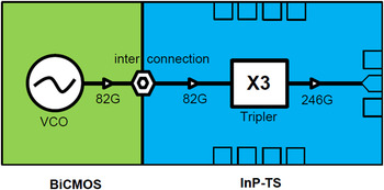
Figure 1 shows the block diagram of the hetero-integrated frequency source, consisting of a VCO and a frequency tripler. The combined process consists of three major steps. First, the desired circuits in BiCMOS technology are processed. The second step consists of BiCMOS wafer planarization and pre-processing of the InP circuits, plus bonding them in a wafer-level BCB bonding process [Reference Kraemer8]. The last step consists of realization and full processing of the circuits in TS InP-DHBT technology. In this step also all interconnects between the two technologies are defined with a suitable via technology.
Block diagram of the hetero-integrated frequency source.

The hetero-integration is performed with a 0.25 µm BiCMOS technology and SiGe npn-HBT devices exhibiting f t /f max = 180/220 GHz and with a 0.8 µm TS InP-DHBT technology, which offers f t /f max values of 360/360 GHz for a one-finger device with 0.8 × 5 µm2 emitter area. The BiCMOS process exhibits a total of five metal layers including three Al metal layers and two Al top-metal layers with 2 and 3 µm thickness, respectively. The TS InP DHBT technology has three Au metal layers with 1, 1.5, and 4.5 µm thickness, respectively. The InP wafers have diameters of 3 inch, which requires that four 3 inch substrates are cored from a processed 8 inch BiCMOS wafer.
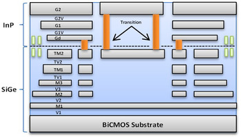
The benzocyclobutene based adhesive wafer bond process between InP and BiCMOS is run at a moderate temperature of 240°C. Therefore, little, if any impact is expected on the active BiCMOS devices. However, significant wafer bow occurs during this process due to the mismatched thermal expansion coefficients of InP and Si substrates. All active Si devices were investigated before and after wafer bonding and it was found that the standard deviation of the f t and f max values of the two different HBT transistors npn1 and npn2 included in this technology is 1 or 2% for a cored 3″ wafer. The performance of the transistors was also checked by using current-mode logic type ring oscillators. There are nine different ring oscillators on every die. Four ring oscillators based on npn1 and five for npn2. The ring oscillator consists of 53 transistor stages in series. The homogeneity over the wafer was checked by measuring the ring oscillator with the smallest gate delay time on every die. The gate delay time per gate is 4.328 ps with a standard deviation of 0.013 ps, corresponding to 0.3% for the 3″ wafer. That exemplifies the excellent yield and homogeneity of the BiCMOS process [Reference Lisker9]. The behavior of the BiCMOS-bonded InP DHBT was compared with DHBTs fabricated in a similar CTE-matched InP-on-AlN process, showing negligible difference [Reference Weimann10]. Yield of hetero-integrated DHBTs could be shown to support realization of small-scale integrated analog circuits containing tens of DHBTs, suitable for the targeted application [Reference Weimann10]. Figure 2 shows the layer arrangement of the hetero-integrated technology, together with the standard transition between the two technologies. The upper part contains the InP metal layers (levels Gd, G1, and G2), the lower part the BiCMOS metal layers (levels M1…TM2). Vias between the InP technology and the BiCMOS metallizations form the transition between the two technologies.
Layer stack of the hetero-integrated semiconductor technologies.

In order to minimize losses for the BiCMOS circuits, a thin-film microstrip line (TFMSL) with M1 and TM2 as ground and signal line, respectively, is used. Stacking of the InP circuits on top of the BiCMOS circuits will result in a detuning of the BiCMOS circuits, in our case the VCO's resonant frequency. Due to the low permittivity of BCB (ε r = 2.65), this effect can be kept at a minimum by avoiding any ground layer in the InP stack (Gd layer) in the vicinity of frequency sensitive BiCMOS structures. However, since the fields of the BiCMOS structures are concentrated within the CMOS dielectric stack, the influence is not critical anyway and it can be eliminated by taking into account the InP stack on top in the BiCMOS design. In the InP part, Gd and G2 are employed as a ground and signal line for the TFMSL, respectively.
The performance of the hetero-integrated technology does not only depend on the individual circuit performance but also on the characteristics of the interconnects and transmission lines in the respective technologies. Therefore, careful investigations are needed considering these issues. There are various types of transmission line configurations possible in this technology [Reference Lisker9], including stripline, tri-state, and high-impedance microstrip lines. Presently, as described above, both TFMSL lines are employed in the InP and the BiCMOS part in order to keep transmission-line loss at a minimum. Accordingly, the interconnect needs to be realized between the signal lines on InP and BiCMOS (topmost metal layer G2 and TM2), while the ground on InP (Gd metal layer) is connected to the ground on BiCMOS (M1 metal layer). A detailed description of hetero-integrated process can be found in [Reference Kraemer8].
III. BICMOS-TO-INP TRANSITION
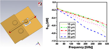
In the hetero-integrated circuit design, the transitions between BiCMOS and InP part represent one of the most important features. The main issues are to optimize them with regards to misalignment between the BiCMOS and InP wafers and to parasitic effects. Optimization is performed by electromagnetic (EM) simulations employing the three-dimensional solver computer simulation technology (CST) Microwave Studio. The parameters available are via diameter, landing pad, and ground opening sizes. The influence of the latter one is rather strong due to the capacitance between the landing pad of the signal line on the TM2 level and the ground (M1 GND). To avoid the capacitance to M1 GND a square opening is realized with an optimum width of 25 µm (see Fig. 3).
Transition region (left) and IL for different sizes of the GND opening in M1 (right).

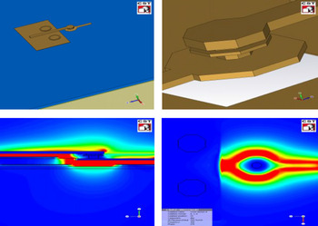
Figure 4 presents details of the transition with all vias in the successive layers. The field plots show the magnitude of the E-field along the line (Fig. 4 bottom left) as well as the same field in the region of the signal via in the ground layer (GD) level of the InP process (Fig. 4 bottom right).
Transition region (top left) and detail of signal via consisting of several successive vias in the different layers (top right). Magnitude of E-field in the longitudinal cross-section (bottom left) and magnitude of E-field around the signal via in the GD level of the InP process (bottom right).

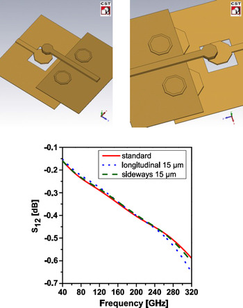
Another major problem in the design is the possible shift of the layers in the InP process relative to the structures of the BiCMOS process, caused by misalignment during wafer bonding. But even if one considers a maximum of 15 µm shift in any direction, the resulting changes remain negligible (see Fig. 5).
Influence of misalignment between InP and BiCMOS wafers: InP layers shifted sideways by 15 µm (top left) and InP layers shifted longitudinally by 15 µm (top right). IL for shifted and standard version against frequency (bottom).

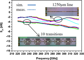
The resulting interconnects performance is excellent: EM simulation data and experimental verification show that a back-to-back structure with two interconnects including a line of 1250 µm length in BiCMOS exhibits a return loss (RL) above 12 dB from DC to 220 GHz and an insertion loss (IL) below 1 dB up to 220 GHz [Reference Ostermay11]. In a more-in-depth investigation, the fabrication of the transitions has been verified for potential misalignment and connection errors using a test structure with a chain of 10 transitions, as illustrated in Figs 2 and 6. For comparison, a further structure with a 1250 µm long transmission line length is included. The structures were characterized from 220 to 325 GHz. Figure 6 presents the measured and simulated insertion loss (S 21) data of the test structure (transition chain with 10 transitions) and the 1250 µm long line (G2) on the InP part. One observes that simulation and measurement for the respective structures are in good agreement. Figure 6 show also the measured insertion loss (S 21) of three samples across the wafer. In order to obtain the IL per transition, it is necessary to subtract the losses of the 1250 µm transmission line and to divide by the number of transitions. This leads to an estimated IL of less than 0.5 dB per transition from 220 to 325 GHz also the measured IL (S 21) of three samples across the wafer.
Simulated and measured IL (S21) of the test structure with 10 concatenated transitions between the InP microstrip layer (G2) and the metal layer (TM2) in the BiCMOS process. The vias close to the InP microstrip line ensure that a common ground is shared between the InP and BiCMOS circuit parts. Also shown are simulated and measured IL data of a 1250 µm line length on the InP part.

These results demonstrate that reliable low-loss mm-wave and sub mm-wave transitions between the BiCMOS and InP technologies are feasible with the MMIC process used. Hence, the signal transitions between the different technologies in heterogeneous integration are not a limiting factor for system performance anymore.
IV. CIRCUIT DESIGN
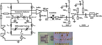
Figure 7 presents the simplified schematic diagram of the hetero-integrated signal source. The circuit is based on a fundamental BiCMOS oscillator featuring a differential Colpitts topology. Special attention has been paid to increase the Q-factor of the tank, in order to minimize phase noise. In the mm-wave range the Q-factor is primarily limited by the varactor and hence series-connected differential metal-oxide-semiconductor varactors with small resistance are employed in the circuit. The VCO is followed by a single-stage buffer in cascode topology offering good isolation and matching [Reference Hossain7]. Single-ended output is taken from one port of the differential buffer.
Schematic diagram of the hetero-integrated source with chip photograph.

The TS InP-DHBT part consists of a 248 GHz single-transistor tripler. The frequency tripler is based on a common emitter, single-ended topology. It uses a 2-finger HBT with an emitter size of 0.8 × 5 µm2 each. The single HBT device is biased under class-A conditions and driven into saturation. In this condition, the HBT amplifier generates an output waveform with higher odd-order harmonics. The unwanted spurious and the fundamental and the second-harmonics are suppressed by a high-pass type output matching network (OMN), followed by an open-short type band-pass filter (BPF). The input matching network (IMN) of the transistor (T) is matched using TRLb1 and TRLb2 to 50 Ω at the input frequency f 0, while the OMN provides conjugate matching at the third-harmonic 3f 0. Moreover, to reduce the losses at the desired harmonic, λ/4 transmission lines TRL1 and TRL2 are used to short-circuit the fundamental f 0 and the second-harmonic 2f 0 of the tripler, respectively [Reference Lewark12]. At the input, a 5 Ω resistor is employed to increase the K factor, thus ensuring stability. A DC blocking 0.5 pF capacitor is included at the input and output to facilitate future integration with buffers or mixers.
At the output, a BPF is used to suppress all unwanted harmonics at the output of the circuit. The transmission lines and the implemented open-short BPF were optimized in advanced design system, assisted by a 2.5D planar EM-simulator (Momentum). The input of the BPF is matched for the third-harmonic impedance and the output of the BPF is matched to 50 Ω.
In Fig. 7 (bottom) shows the chip photograph of the entire hetero-integrated circuit. The VCO circuit can be seen on the left, in the center the BiCMOS-InP transition, and the tripler circuit on the right. The chip area of the hetero-integrated circuit reaches 3 × 1 mm2. DC biasing of the VCO on BiCMOS as well as the tripler on InP DHBTs is both provided through DC pads on top of the chip, i.e. on the upmost InP metallization layer. RF output has to be taken from the ground–signal–ground (GSG) probe pads on the right-hand side of Fig. 7. A continuous ground plane is located between the TS InP on the right-hand side and the BiCMOS circuit area below. This ensures a low loss thin-film microstrip wiring environment in the TS InP part, which is not affected by the BiCMOS circuitry below. The BiCMOS filler structure is implemented only in the BiCMOS circuit part while the InP circuit part is kept filler-free.
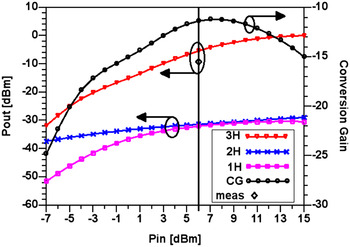
In Fig. 8, the simulated conversion gain (CG) and output powers of the first- (1H), second- (2H) and the desired third-harmonic (3H) are plotted against input power. One can see that the power level of the fundamental and second-harmonic stays −20 dB below the third-harmonic according to simulations. Measured output power of the hetero-integrated source is −9 dBm (see Section Vc), which is not far from the expected value from the simulation.
Triplr circuit of Fig. 7: Simulated CG and output power of the first-harmonic (1H), second-harmonic (2H) and the desired third-harmonic (3H) as a function of input power for 82.66 GHz fundamental frequency. Actual input power was measured to be about 6 dBm, as indicated by the vertical bar. Also included is the measured output power at third-harmonic (diamond).

In the circuit realized here, a version of the tripler without the BPF was implemented. After fine tuning the IMN and OMN, the tripler without the BPF in simulation predicts −3.2 and + 2.1 dBm single ended output power, for an input power of 6 and 14 dBm, respectively. The tripler collector bias voltage and base current were set to 1.6 volts 10 and 0.27 mA, respectively. According to simulations, the fundamental (f 0) and the second-harmonics (2f 0) were suppressed by approximately −10 and −19 dB compared with the third-harmonic (3f 0). It is obvious that the filter involves a trade-off between harmonics suppression and insertion loss and thus output power for the wanted harmonic. The latter could be compensated by adding an extra buffer stage at the output of the tripler. Regarding power, one should note also that the circuits involves a 535 µm long interconnect line between the VCO and the tripler (see Fig. 7), which could be significantly shortened in a redesign thus improving output power further.
V. MEASURED PERFORMANCE
A) Setup
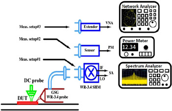
The hetero-integrated source was measured on-wafer using the setup shown in Fig. 9. Three major steps were performed to characterize the hetero-integrated source. In a first setup, the output spectrum of the complete hetero-integrated circuit was investigated with a Cascade GSG on-wafer waveguide probe, radiometer physics GmbH sub-harmonic mixers (SHM), and a FSUP (model name) Rhode and Schwarz (R&S) signal source analyzer. The goal here was to identify and measure the output frequency and to guarantee that the spectrum is clean, i.e. the amplitudes of the spurious lines is small enough, which is important for the accuracy of the power measurement. To estimate suppression of unwanted harmonics over the full frequency range, different frequency bands of the output spectrum were measured applying the suitable waveguide probes and sub-harmonic mixers with the same setup.
Measurement setup for characterization of the signal source (meas. setup #1 for output spectrum, meas. setup #2 for power measurement, meas. setup #3 for S parameters).

In a second setup, the output power of the circuit was determined with a waveguide probe and a waveguide system connected to the input of an Erickson PM4 power meter. Since the power meter is not frequency-selective any spurious line will degrade measurement accuracy of the component at the wanted output frequency.
In a third setup, the output reflection coefficient of the circuit was measured with a waveguide probe and an R&S ZVA-Z325 frequency extender connected to the input of a vector network analyzer.
B) The BiCMOS VCO after the full process
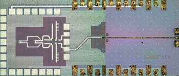
In order to determine the behavior of the BiCMOS VCO itself and the possible changes due to wafer bonding and the additional layers on top of the CMOS stack, a version without tripler was fabricated where the InP circuit part consists of a simple thru-line (see Fig. 10). This allows on-wafer probing. In this case, the frequency of oscillation was measured using an FSUP signal source analyzer. In order to ensure linear operation of the SHM, a variable attenuator was placed right after the RF probe, with attenuation fixed to 20 dB during measurement of the VCO spectrum.
Chip photograph of the 82 GHz VCO without InP tripler (the InP part consists of a simple through-line).

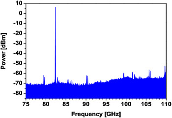
The output power of the circuit was measured with a 90° bend and WR10 taper connected to the input of an Erickson PM4 power meter. Figure 11 shows the VCO output spectrum. The VCO was fed by 5 volts DC supply and the current consumption was 134 mA.
Measured output frequency spectrum of the VCO version without tripler according to Fig. 10. (tuning voltage: 0 volt; losses of cable, prober, 20 dB attenuator and of the 1 mm long microstrip line on the chip deembedded).

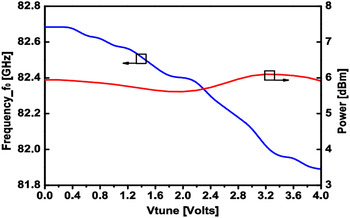
The measured output power of the VCO was approximately 5 dBm, with around 1 GHz of tuning range and a corresponding output power variation of less than 0.3 dB. Correcting the output power by the loss of the 1 mm long microstrip line at the output (see Fig. 10), one obtains approximately 6 dBm of actual input power delivered to the tripler in the final circuit (see following subsection) Fig. 12 shows the output power and frequency of oscillation as a function of the tuning voltage. Note that in Fig. 11 taking in to account all the losses, the output power measured on spectrum analyzer is in good agreement with the measured actual output power shown in Fig. 12.
Measured output power and frequency of the VCO (see Fig. 8) as a function of tuning voltage (waveguide system and prober loss deembedded).

C) The hetero-integrated source
The hetero-integrated source was characterized on-wafer with the setup illustrated in Fig. 9.
A GSG (i325-S-GSG-50-BT) WR3.4 waveguide probe was used to probe the output signal in the band from 220 to 325 GHz. The IL of the output probe is 4.5 dB as given by the vendor; waveguide bend and taper are estimated to contribute 3 dB ILs in the 245 GHz band. All measurement data presented in the following are corrected by the resulting attenuation of 7.5 dB.
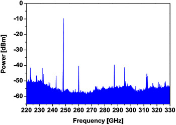
The output spectrum was detected by means of a sub-harmonic spectrum analyzer mixer WR3.4, which has a conversion loss of approximately 35 dB at 245 GHz, and an FSUP signal source analyzer. Figure 13 presents the measured output spectrum.
Measured output frequency spectrum of the hetero-integrated source (tuning voltage: 0 volts, cable and prober loss deembedded).

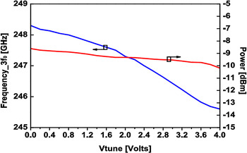
In a next step the output power of the circuit was determined with a 90° bend and a WR3.4-WR10 taper connected to the input of an Erickson PM4 power meter. Taking into account the waveguide system and probe loss, one obtains an actual output power of −9 dBm at the circuit output, at a frequency of 248 GHz. In Fig. 14, the output frequency of the hetero-integrated source and the output power are plotted as a function of the tuning voltage. A tuning range around 3 GHz is achieved. One should note that the deembedded power data for the spectrum and the power meter measurements in Figs 13 and 14 agree well, although measurements set-ups differ (see Fig. 9, setup #1 and #2). This proves repeatability of our measurements and supports validity of the deembedding approach.
Measured output frequency and power of the hetero-integrated source as a function of the tuning voltage (waveguide and prober loss deembedded).

The frequency tuning characteristics plotted in Fig. 12 and the corresponding fundamental Fig. 14 differ slightly by 200 MHz because they refer to different circuits on the wafer. The standard deviation of the BiCMOS VCO frequency across the 3″ hetero-integrated wafer is 0.08% [Reference Lisker9], i.e. 66 MHz.
The BPF at the output introduces approximately 4 dB losses (estimated by EM simulation), therefore, the tripler circuit alone is expected to deliver about −5 dBm. On the other hand, the BPF improves suppression of fundamental (f 0) and second (2f 0) harmonics by more than 25 dB (estimated by EM simulation), which is advantageous from the system point of view.
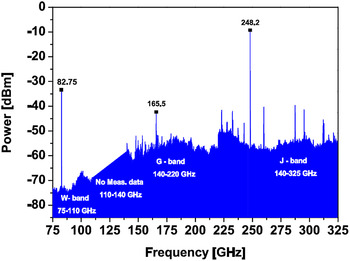
In order to obtain comprehensive results on spectral purity and unwanted harmonics suppression, three different bands (W, G, and J) have to be measured. This was performed by using a WR-10 waveguide system (probe and SHM), a WR-5 waveguide system (probe and SHM) and a WR-3 waveguide system (probe and SHM) separately. Figure 15 provides the measured output spectrum at W-band, G-band, and J-band. Due to the presence of spurious signals caused by the mixers etc. interpretation of the data is not always straightforward. In J-band and W-band, however, all unwanted or spurious signals are much weaker than the third- and first-harmonics, respectively. Thus, measuring the total power in these bands with the power meter should give reliable values for the harmonic lines.
Measured W-band, G-band and J-band output frequency spectrum of the hetero integrated source (tuning voltage: 0 volt, cable and prober losses deembedded; no measured data in the frequency range between 110 and 140 GHz).

One can easily observe that the fundamental (f 0), second-harmonic (2f 0) and unwanted signals all are below −30 dB with respect to the desired third-harmonic (3f 0) signal. Note that in Fig. 15 the back ground noise of the spectrum increases in the higher frequency bands. This is due to the noise contribution from the sub-harmonic mixer used for the G and J bands.
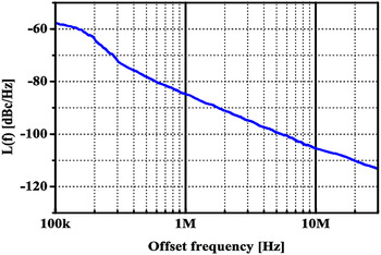
The measured phase-noise characteristics are presented in Fig. 16. Values of −85 and −106 dBc/Hz at offsets of 1 and 10 MHz are obtained, respectively. These are excellent results for this frequency range and a free-running VCO.
Measured phase noise performance of the hetero-integrated source.

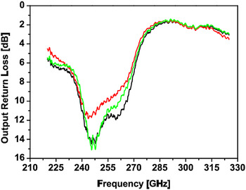
The output RL of the hetero-integrated circuit was measured using a vector network analyzer. The system was calibrated with thru-reflection-match to place the reference plan at the probe tips. Note that in this measurement the bias supply of the BiCMOS VCO was switched off so that the InP tripler was operating as a non-autonomous circuit. Figure 17 shows the measured output RLs of three samples. The curves indicate broad-band behavior with more than 12 dB RL over at least 20 GHz. This is a promising result at this frequency range. It also shows that all unwanted harmonics (f0, 2f0) and spurious signals are well suppressed by the integrated BPF at the output.
Measured output RLs of the hetero-integrated source (three samples).

The output power can certainly be increased by using additional input and output buffer stages in the tripler circuit. Also, it is important to note that the hetero-integrated technology employed here (250 nm-BiCMOS and 800 nm-InP) has a more relaxed geometry compared with most other circuits published, e.g. [Reference Lai13–Reference Krozer24].
VI. CONCLUSION
This paper presents a voltage controlled 248 GHz hetero-integrated source in InP-on-BiCMOS technology, which consists of an 82.7 GHz VCO in 0.25 µm BiCMOS technology and a 248 GHz frequency tripler in 0.8 µm TS InP-HBT technology. The source delivers −9 dBm output power with −85 dBc/Hz phase noise at 1 MHz offset. It is confirmed that the hetero-integrated technology offers not only the combination of BiCMOS and InP circuits but also broadband low loss transitions between them up to 325 GHz. This opens up application fields where designer can take the advantages of both InP and Silicon technology, e.g. one does not need to choose a small BiCMOS node but can nevertheless reach excellent mm-wave behavior, using the InP components. This also paves the way for further increasing frequency towards the THz range.
ACKNOWLEDGEMENT
The authors would like to acknowledge partial financial support by the Leibniz Association through the SAW project “HiTeK” and the project “Science Fab für heterointegrierte InP/BiCMOS Höchstfrequenz-Systeme” by the Leibniz Association.
 Maruf Hossain received his M.Sc. degree in Electronics/Telecommunication from the University of Gavle, Gavle, Sweden, in 2008. In 2008, he joined IHP microelectronics in the circuit design department, Frankfurt/Oder, Germany.
Since 2011, he has been with the Ferdinand-Braun-Institut (FBH), Berlin, Germany. His research interests include the CMOS, millimeter wave and THz MMIC circuit design and characterization.
 Ina Ostermay joined Ferdinand-Braun-Institute in 2011, where she works on heterogeneous device integration. She received her Ph.D. degree from TU Dresden in 2013 and is responsible for thin film deposition in the process technology department.
 Nils G. Weimann (M'99) received his Diploma degree with honors in Physics from the University of Stuttgart, Germany, in 1996, and the Ph.D. degree in Electrical Engineering from Cornell University, Ithaca, NY, USA in 1999. He then joined Alcatel-Lucent Bell Labs in Murray Hill, NJ, as a Member of Technical Staff, and in 2003 became a Technical Manager there. Since 2012 he has been with the Ferdinand-Braun-Institut in Berlin, Germany, where he is now leading the THz Components research group. His research interests include compound semiconductor technology and terahertz electronic components and circuits.
 Franz Josef Schmueckle (M'94) received his Dipl.-Ing. (FH, TH) and Dr.-Ing. degrees in Electrical Engineering from Fern Universität Hagen, Hagen, Germany. His current research interests include EM simulations of microwave packaging problems.
 Johannes Borngraeber received his Diploma in Mathematics from Humboldt University, Berlin, Germany, in 1981. Since 1994, he has been working in the Department of Circuit Design at IHP Microelectronics GmbH. Currently he is especially interested in noise figure and phase noise measurement techniques in the millimeter-wave range.
 Chafik Meliani received his Ph.D. degree in Electrical Engineering in 2003. From 2000 to 2003, he was with Alcatel in Paris, working in the design of high bitrate circuits for optical communication systems. In 2003, he joined the Ferdinand-Braun-Institut fürHöchstfrequenztechnik (FBH) in Berlin, where he was involved in IC design for communication and radar systems. From 2008 to 2011, he was leading the power amplifier group at FBH. In 2012, he joined the Leibniz Institut für Innovative Mikroelektronik (IHP), where he heads the mm-wave wireless group. His current research interests include millimeter-wave circuit design and characterization.
 Marco Lisker received his Ph.D. degree from Otto-von-Guericke University, Magdeburg, Germany, in 2001. He has been a Process Engineer and a Research Staff Member of IHP, Frankfurt/Oder, since 2009.
 Bernd Tillack received his Ph.D. degree from the University Halle-Merseburg in 1980. In 1981, he joined the IHP Frankfurt (Oder), Germany, as a staff member of the process technology. He had been the project leader of different IHP Si/SiGe technology projects. His research interests include SiGe BiCMOS technology development following the “More than Moore” strategy for embedded system applications. Since 2004, he is in charge of the Si/SiGe process and device technology in the IHP. In 2008, he got a professorship for Si-based high-frequency technologies at the Berlin Institute of Technology (TU Berlin).
 Olaf Krueger received his Ph.D. degree in Chemistry from Humboldt-University Berlin, Berlin, Germany, in 1993. Since 2001, he has been with the Ferdinand-Braun-Institut, Leibniz-Institut für Höchstfrequenztechnik (FBH), Berlin, where he is currently Head of the Process Technology Department. His current research interests include novel techniques for device assembly.
 Viktor Krozer received his Dipl.-Ing. and Dr.-Ing. degrees in Electrical Engineering at the Technical University Darmstadt in 1984 and in 1991, respectively. In 1991, he became senior scientist at the TU Darmstadt working on high-temperature microwave devices and circuits and submm-wave electronics. From 1996 to 2002, Dr., Krozer was Professor at the TU Chemnitz, Germany. From 2002 to 2009, he has been Professor at Electromagnetic Systems, DTU Elektro, Technical University of Denmark, and was heading the Microwave Technology Group. Since 2009, Dr., Krozer is the endowed Oerlikon-Leibniz-Goethe professor for Terahertz Photonics at the Johann Wolfgang Goethe University Frankfurt, Germany and group leader for Terahertz Electronics at the FBH, Germany. His research areas include terahertz electronics, MMIC, nonlinear circuit analysis and design, device modeling, and remote sensing instrumentation.
 Wolfgang Heinrich received his Diploma in Electrical Engineering, the Ph.D. (Dr.-Ing.), and the Habilitation degree from the Technical University of Darmstadt, Germany. Since 1993, he has been with the Ferdinand-Braun-Institut (FBH) at Berlin, Germany, where he is the Head of the Microwave Department and Deputy Director of the Institute. Since 2008, he is also professor at the Technical University of Berlin. His present research activities focus on MMIC design with emphasis on GaN power amplifiers, mm-wave integrated circuits and packaging, and electromagnetic simulation.