Introduction
In recent years, various techniques have been developed for designing low radar cross-section (RCS) antennas using radar absorbing materials [Reference Fante and McCormack1], holographic metasurfaces [Reference Long, Jiang and Gong2], metamaterials [Reference Ren, Jiang and Gong3], metasurfaces [Reference Puneeth Kumar, Karthik and Krishnamoorthy4], and electromagnetic band-gap (EBG) structures [Reference Chen, Balanis and Birtcher5]. Fante and McCormack [Reference Fante and McCormack1] have explored combinations of electric and magnetic Salisbury screens for reducing reflections. A high directivity, low RCS-slotted patch antenna using holographic metasurface and partially reflecting surface has been proposed in [Reference Long, Jiang and Gong2]. Cross-shaped polarization conversion metamaterial has been used to reduce RCS significantly over a wider band in [Reference Ren, Jiang and Gong3] has presented a slotted antenna with thin rectangular patch artificial magnetic conductor (AMC) for wideband reflection cancellation to reduce RCS. Polarization-dependent metasurface is proposed in [Reference Puneeth Kumar, Karthik and Krishnamoorthy4] that reduces in-band RCS. In [Reference Chen, Balanis and Birtcher5, Reference Zheng, Guo, Vandenbosch and Ding6], checkerboard-patterned EBG surfaces have been designed to reduce wideband RCS. Shi et al. [Reference Shi, Zhang, Meng and Li7] have utilized a 2 × 2 antenna subarray with polarization rotation characteristics for the RCS reduction (RCSR). Some of the designs involve two substrates with aperture coupling feed [Reference Balanis8]. Zhang et al. [Reference Zhang, Li, Zheng, Ding and Guo9] have proposed the current direction slots subtraction technique to obtain the wideband RCSR. Liu et al. [Reference Liu, Li, Jia, Zhang and Zhou10] have proposed a wideband low-RCS patch antenna based on a holographic metasurface. A wideband RCSR technique with a slot-coupled patch antenna using AMC structure is proposed in [Reference Xue, Jiang and Gong11]. Huang et al. [Reference Huang, Wan, Wang and Ma12] have implemented slotted frequency selective surface (FSS) ground to obtain low RCS. In [Reference Zheng, Guo, Li and Ding13], a polarization conversion metasurface composed of two oblique triangle split rings that reduce RCS in broadband is proposed. A high-gain, wideband mushroom antenna with low RCS is proposed in [Reference Jia, Liu, Wang, Li and Gong14] implementing bandstop FSS in place of metallic ground. A phased array antenna based on the switchable-stacked artificial structure is proposed in [Reference Ding, Cheng, Shao and Wang15] to obtain broadband RCSR and wide scanning range. Both in-band and out-of-band RCSR techniques were proposed in [Reference Zhang, Xu, Qu, Ding and Guo16] by replacing the weak current distribution ground plane region with 14 square slots.
In this paper, a novel design to achieve in-band RCSR and polarization rotation is presented. The cross-shaped unit cell is patterned on the metal layer and sandwiched between two dielectric layers: RO3003 with dielectric constant 3 at top and RT Duroid 6010 with dielectric constant 10.2 at the bottom, to achieve zero reflection phase and significantly low values of reflection and transmission coefficient around 8.25 GHz. FSS with different orientations of the EBG unit cells is analyzed and designed to obtain good absorptivity near 8.25 GHz. The paper has fabricated a coaxial probe-fed circular patch antenna resonating at 8.25 GHz at the top layer. It has placed four identical circular patches at the four corners of the same layer. Each of the corner patches is coupled with two orthogonally aligned and diagonally interconnected feed lines at the bottom-most layer for polarization rotation of the backscattered electromagnetic (EM) wave. The high absorptivity of the FSS layer lowers the in-band RCS to −21.4 dBsm. The proposed antenna offers a gain of 6.72 dB. Incident energy is backscattered into eight directions separated by ϕ = 45°. The proposed antenna has the RCSR band of 7.7–13.3 GHz and −10 dB RCS band of 7.7–9.4 GHz. It offers normalized polarization rotation ratio (PRR) more than 0.8 within −40° to + 40° angular region within the frequency band 8–8.5 GHz. The measured result using the fabricated prototype agrees well with the simulated one.
Development of EBG unit cell and FSS
EBG unit cell
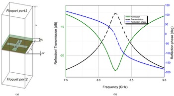
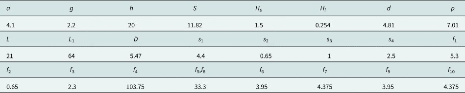
EBG behavior can be characterized by the reflection phase property. In Fig. 1(a), master and slave boundaries are considered at the pair of opposite side walls to ensure the periodic nature of the unit cell. Two floquet ports were considered at the top and bottom faces which help us to check the reflection magnitude and phase properties as well as the transmission properties as in Fig. 1(b). The EBG unit cell consists of cross-shaped slots etched over a metal plane which is sandwiched between two different substrates as shown in Fig. 1(a). The upper substrate utilizes RO3003 material having dielectric constant 3, thickness 1.5 mm, and dissipation factor 0.001 at 10 GHz. The bottom layer contains RT Duroid 6010 material with a dielectric constant of 10.2, a thickness of 0.254 mm, and a dissipation factor of 0.0023 at 10 GHz. The dimension of the cross-shaped slots is optimized and shown in Table 1. Parametric analysis is carried out to tune the resonant frequency to achieve the minimum reflection magnitude and zero reflection phase. It is seen that the designed unit cell has a reflection magnitude of −25.24 dB and 0° reflection phase at 8.25 GHz as shown in Fig. 1(b). The −10 dB impedance bandwidth is 0.81 GHz and the band lies from 7.86 to 8.67 GHz.
(a) EBG unit cell and (b) reflection magnitude and phase of EBG unit cell.

Dimensions of EBG unit cell, single element and 2 × 2 array (unit: mm)

EBG arrays and their absorptivity
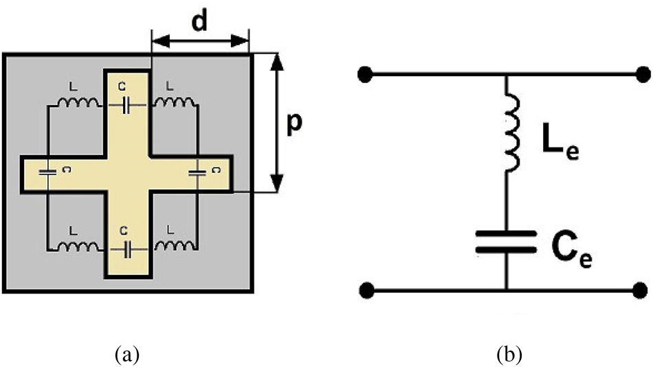
The equivalent circuit of the unit cell is shown in Fig. 2. Unit cells can be best described with an LC circuit. The cut-out portion creates a capacitive region whereas the conductive metal portion constitutes an inductive region. Therefore, it can be represented with an LC circuit. The effective inductance L e and capacitance C e shown in Fig. 2(b) account for the equivalent of the four inductors and capacitors shown in Fig. 2(a) respectively.
(a) Circuit elements over the EBG unit cell and (b) equivalent circuit of the EBG unit cell.

The resonant frequency of the unit cell can be expressed as shown in equation (1):

The equivalent circuit model analysis and the equations are based on [Reference Ferreira, Caldeirinha, Cuiñas and Fernandes17]. The inductance and capacitance in equation (1) are guided by the width and the length of the vertical strip respectively. The spacing between the two consecutive cross-shaped unit cells does not affect the resonating frequency but controls the bandwidth. The choice of d/p ratio also has a significant impact on the capacitance C and thereby affects the resonance.
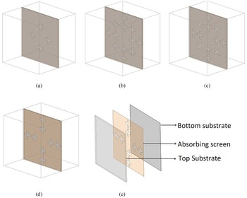
The EBG unit cells are placed on the sandwiched metal layer differently and four different FSSs are obtained as shown in Fig. 3. FSS1 has four unit cells oriented 90° to each other around the center patch as shown in Fig. 3(a). FSS2 has 12 unit cells covering the entire ground plane except the patch regions as shown in Fig. 3(b). FSS3 is the same as FSS2 with four unit cells tilted around the z-axis by 45° as depicted in Fig. 3(c). FSS4 derived from FSS3 by removing the tilted unit cells as shown in Fig. 3(d). From the knowledge of reflection and transmission coefficients S 11 and S 21, we can estimate the absorption [Reference Sanz-Fernandez, Cheung, Goussetis and Mateo-Segura18]. Absorptivity is calculated based on equation (2):

Absorbing surfaces: (a) FSS1, (b) FSS2, (c) FSS3, (d) proposed FSS4, and (e) different layers of FSS4.

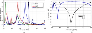
The absorptivity of the FSS layers is shown in Fig. 4(a). According to Fig. 4(a), the normalized absorption maxima of the FSS layers occur at 8.05, 8.19, 8.3, and 8.26 GHz. The variation in frequency arises due to the slight change in the equivalent inductance and capacitance in different configurations. Out of the four FSS layers, FSS4 that corresponds to the absorptivity maxima at 8.26 GHz has been chosen as it is closest to the desired frequency 8.25 GHz. The reflection and transmission properties of the FSS4 are shown in Fig. 4(b) which shows a small reflection magnitude and a good transmission at 8.25 GHz.
(a) Normalized absorption of four FSSs and (b) reflection and transmission properties of FSS4.

Antenna design
Circular patch
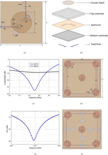
The single element which is shown in Fig. 5(a) is fed with two orthogonal feed lines (ports are shown in Fig. 5(a)) are positioned at the bottom layer of the lower substrate to achieve dual-polarization. Two I-shaped apertures are patterned on the sandwiched metal layer to provide the coupling of EM energy from the feed line to the patch. The stacking of different layers is shown in Fig. 5(b). The dimensions of the aperture and the patch are optimized so that the single element resonates at 8.25 GHz as presented in Fig. 5(c). The shape and dimensions of the apertures affect the resonating frequency and the degree of coupling. In this study, the optimization of the apertures is performed and found that the I-shaped apertures provide good impedance matching at 8.25 GHz. So, it is chosen for the proposed design.
(a) Single element, (b) stacking of different layers, (e) S-parameters of single element, (c) co-axial probe fed 2 × 2 antenna array, (d) S 11 of coaxial probe fed 2 × 2 antenna array, and (f) overall proposed design showing the I-shape apertures, feeds, and EBG surface FSS4.

A coaxial probe-fed circular patch antenna is optimized to resonate at 8.25 GHz and placed on the top of the upper substrate is shown in Figs 5(d) and 5(e). Subsequently, four identical circular patches are placed on the four corners of the same layer each of which is fed through two feed lines orthogonally embedded at the bottom layer of the lower substrate. These single elements are placed at the four corners and are interconnected diagonally as shown in Fig. 5(d). Because of this arrangement, the position of each pair of feed lines is 90° rotated. As a result, it works as a polarization rotation surface (PRS). FSS4 layer as shown in Fig. 3(e) has been included in the sandwiched metal layer to improve the RCS. Figure 5(f) shows the overall proposed design including antennas, I-shape apertures, feeds, and the EBG surface FSS4 on the sandwiched metal layer.
The S 11 of the single element is presented in Fig. 5(c). In the design, the two feed lines are oriented orthogonal to each other and diagonally connected as shown in Fig. 5(d). This feeding structure generates horizontal-, vertical-, and circularly-polarized waves. To generate the circularly polarized wave, two ports are excited with a phase difference of 90°. I-shape aperture is obtained by adding two small slots at the ends of the rectangular aperture. Slot lengths are optimized so that the impedance matching and the degree of coupling to patch become maximum [Reference Pous and Pozar19]. Table 1 shows the dimensions indicated in Figs 5(a) and 5(d).
PRS by using 2×2 array
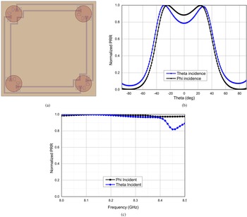
In the proposed model, the backscattered energy is rotated by four circular patches located at the four corners. The two feed lines and apertures of each circular patch are 90° rotated anticlockwise direction. The rotated single element is translated to the next corner in the clockwise direction. This procedure is repeated for four patches. Feed lines of the diagonal elements are interconnected as shown in Fig. 6(a). The vertically aligned feed of one element is connected to the horizontally aligned feed of another diagonal element and vice versa. With this arrangement, the 2 × 2 array exhibits a polarization rotation feature.
(a) 2 × 2 array, (b) PRR versus theta plots, and (c) PRR versus frequency plots.

The polarization rotation feature can be verified by a metric called polarization rotation ratio (PRR) [Reference Shi, Zhang, Meng and Li7]. PRR is mathematically defined as the ratio of theta component of backscattering RCS to the total backscattering RCS when a phi polarized electric field is incident on the antenna. To check the polarization rotation feature, a plane wave with phi and theta polarizations is allowed to fall normally on the 2 × 2 array and the results are plotted as shown in Fig. 6. The normalized PRR plot is almost the same for both the theta and phi incidence waves. Furthermore, normalized PRR is more than 0.9 for ϕ-incident wave and it is more than 0.8 for θ-incident wave as elevation angle θ varies from −40° to +40° and frequency varies from 8.0 to 8.5 GHz as shown in Figs 6(a) and 6(b).
Results and discussion
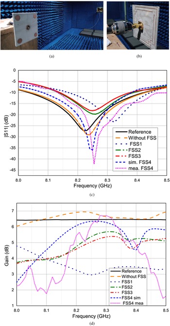
The proposed antenna model is simulated and designed by using Ansys HFSS electromagnetic simulation software. Later it was fabricated by using a PCB prototype machine. Measured results are obtained by using Anritsu MS2037 VNA master. To measure the radiation pattern, the antenna is placed in an anechoic chamber whose walls are fully covered with pyramidal-shaped absorbers to ensure free field condition. The measurement setup is shown in Fig. 7. The front view of the fabricated model is shown in Fig. 7(a) and the back view is shown in Fig. 7(b). In our study, we have considered four FSS surfaces where unit cells are oriented in different fashions as shown in Fig. 3. Among all, FSS4 offers the highest absorptivity according to Fig. 4(a) and allows sufficient space for the absorption of the incident energy within the regions of the EBG cells, and stimulates backscattering in the regions where EBG cells are absent. As a result, we obtain four regions of absorption and four regions of backscattering, and thereby it produces eight backscattering lobes with a small lobe at the center. In this way, the RCS due to FSS4 improves. However, with the FSS the current distribution gets modified and the gain reduces as shown in Fig. 7. The best trade-off between RCS and gain is obtained with FSS4, so it is considered for the proposed structure. FSS3 is derived from FSS2 by tilting the axes of the four-unit cells by an angle of 45°. Because of this modification, the absorptivity improves significantly as shown in Fig. 4(a), but the gain parameter reduces slightly than FSS2 as shown in Fig. 7(d).
(a) Front view of the proposed antenna inside anechoic chamber, (b) back view of the proposed antenna, (c) S 11, and (d) gain plots with all FSSs.

S 11 and bandwidth
S 11 of the multi-layered EBG antenna with four different FSSs are shown in Fig. 7(c). Coaxial feeding has been applied at a 2 mm offset from the center to provide good impedance matching. Figure 7(c) shows that the antenna with FSS4 offers S 11 of −36 dB at 8.25 GHz. It offers a −10 dB bandwidth of 0.31 GHz from 8.08 to 8.39 GHz. The measured bandwidth of the proposed antenna is 0.37 GHz from 8.13 to 8.5 GHz and the measured S 11 peak is −42.1 dB.
Gain
The gain plots of the fabricated prototype are shown in Fig. 7(d). The gain of the reference antenna is 6.45 dB and is constant for the entire band of interest. When PRS is included, gain enhances to 6.95 at 8.22 GHz. Simulated gain achieved with FSS1, FSS2, FSS3, and FSS4 is 4.02, 5.69, 5.39, and 6.35 dB, respectively. The measured gain with FSS4 is close to that of the simulated gain and its peak value is 6.72 dB at 8.3 GHz and the cross-shaped slots do not degrade the antenna gain.
Radiation pattern
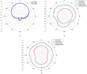
Figure 8(a) shows the radiation pattern of the single element shown in Fig. 5(a). It is seen that the −10 dB bandwidth of the antenna element is 0.45 GHz ranging from 8.0 to 8.45 GHz. From Fig. 6, we can observe the 3 dB beamwidth of the antenna element is ranging from −45° to +45°.
Radiation patterns of (a) single element, (b) co-pol and cross pol in E-plane, and (c) co-pol and cross-pol in H-plane at 8.25 GHz.

The Co-pol and cross-pol radiation patterns in E- and H-planes of the proposed antenna with EBG surface FSS4 at 8.25 GHz are shown in Figs 8(b) and 8(c), respectively. Co-pol and cross-pol patterns are shown in the same plot to show the isolation clearly. The radiation pattern orienting along ϕ = 0° and ϕ = 45° has 3 dB beamwidths of 31° and 146° respectively. This shows that the beam is narrow along ϕ = 0° and wide along ϕ = 45°.
RCS reduction
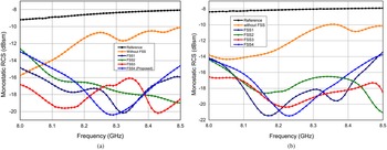
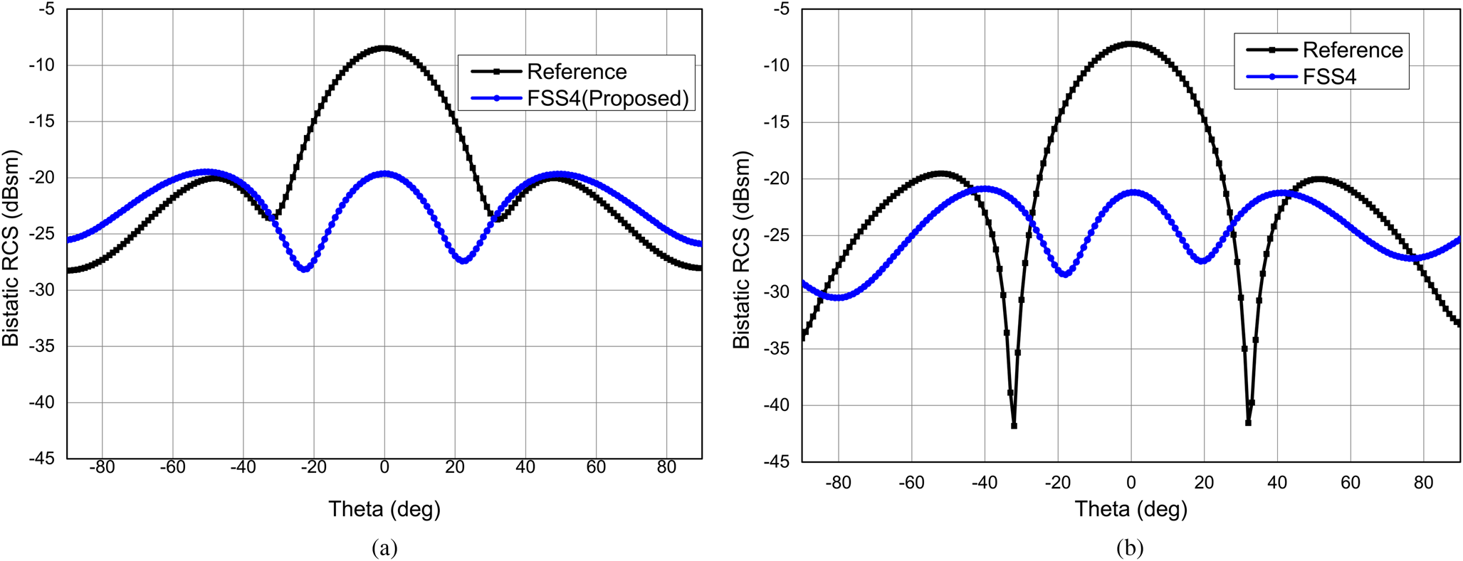
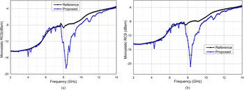
A study on RCSR is conducted by allowing the plane waves with ϕ and θ polarizations to fall normally over the antenna surface. Low RCS for a frequency band of 8–8.5 GHz is shown in the monostatic RCS plots in Figs 9(a) and 9(b). Monostatic RCS plots at 8.25 GHz with theta variation are shown in Figs 10(a) and 10(b). Monostatic RCS plots for a frequency range from 2 to 14 GHz are shown in Fig. 11. From Fig. 11(a), it can be observed that the RCSR maxima is −20.4 dBsm at 8.29 GHz and −19.64 dBsm at 8.25 GHz for a ϕ-incident wave and from Fig. 11(b), it can be observed that RCSR is −21.5 dBsm at 8.3 GHz for a θ-incident wave. It is evident from the figures that there is a maximum RCSR of 12.02 dBsm for a ϕ-incidence wave at 8.29 GHz and 13.39 dBsm reduction for a θ-incidence wave at 8.23 GHz. From Figs 11(a) and 11(b), the total RCSR band and −10 dB RCS bands for both ϕ- and θ-incident waves are 7.7–13.3 GHz and 7.7–9.4 respectively. Therefore, −10 dB RCS bandwidth is 30.35% of the RCSR band and lies within the RCSR band. RCSR is centered around 8.25 GHz and coinciding with the operating band mentioned in Section “S 11 and bandwidth,” thereby achieving the in-band RCSR.
Monostatic RCS comparison of four FSS for a normally incident plane wave with (a) ϕ-incidence and (b) θ-incidence.

RCSR at 8.25 GHz for a normally incident plane wave with (a) ϕ-incidence and (b) θ-incidence.

Monostatic RCS plot for a normally incident plane wave with (a) ϕ-incidence and (b) θ-incidence.

Bistatic RCS lobes
3D Bistatic RCS lobes for a ϕ-incident plane wave for the antenna without FSS, with FSS1, FSS2, FSS3, and with FSS4 at 8.25 GHz are shown in Fig. 12. From Fig. 12(a), we observe that the antenna without FSS will backscatter pointing to θ = 0° through the main lobe. Splitting of the main bistatic lobe takes place when FSS1, FSS2, FSS3, and FSS4 are added as shown in Figs 12(b)–12(e) respectively.
Bistatic RCS lobes of the antenna at 8.25 GHz for a normally incident wave with ϕ-incidence: (a) without FSS, (b) with FSS1, (c) with FSS2, (d) with FSS3, and (e) with FSS4 (proposed).

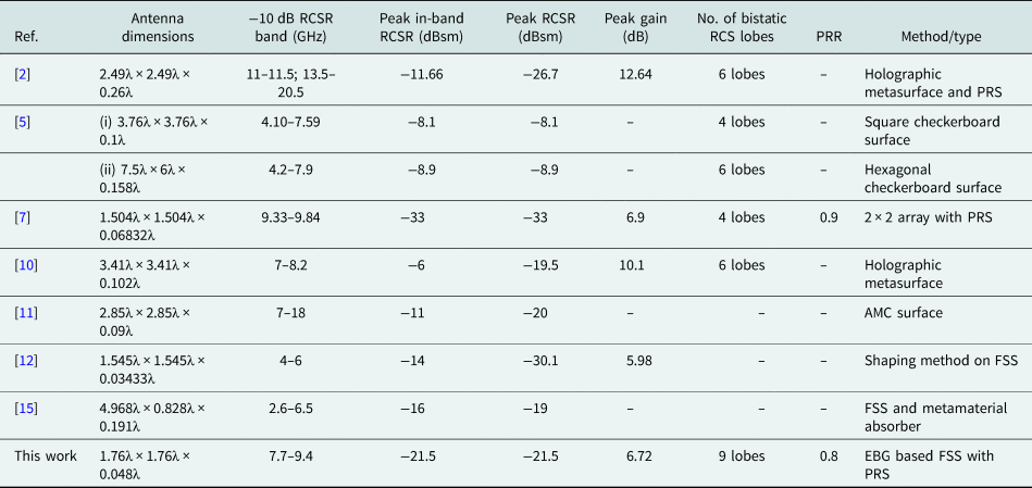
In Fig. 12(b), the three lobes along one diagonal are joined and appear as a single wide lobe. This web joining is reduced in Figs 12(c) and 12(d) as the FSSs are employed with more number of EBG unit cells. In Fig. 12(e), lobes can be seen separately and the effect of web joining is very less in the proposed case. The incident plane waves are backscattered into eight different directions separated by ϕ = 45° with a weak lobe at the center. From Fig. 10(a) we notice that the center lobe has an RCS of −19.65 dBsm at θ = 0° and this reduces to −28.15 dBsm at θ = 23°. The same kind of bistatic lobes is observed in the case of θ-incidence also. We can observe the corresponding bistatic RCSR in Fig. 11(b). The performance of the proposed antenna is compared with the reported models as shown in Table 2.
Comparison with reported models

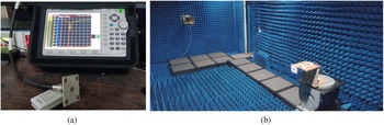
As shown in Table 2, the dimension of the proposed antenna is smaller than that of the other reported models except [Reference Huang, Wan, Wang and Ma12]. Peak in-band RCSR is improved compared to [Reference Long, Jiang and Gong2, Reference Chen, Balanis and Birtcher5, Reference Liu, Li, Jia, Zhang and Zhou10–Reference Huang, Wan, Wang and Ma12, Reference Ding, Cheng, Shao and Wang15]. The number of bistatic lobes is 9. That means the backscattering takes place in nine directions. This number is more compared to any other articles listed in Table 2. The S 11 measurement setup and the setup of the radiation pattern measurement in E- and H-planes for both co-pol and cross-pol measurement at 8.25 GHz are shown in Figs 13(a) and 13(b), respectively.
(a) S-parameters measurement setup and (b) radiation pattern measurement setup inside anechoic chamber.

Conclusion
In this paper, a novel EBG-based in-band RCSR technique is proposed. The absorptivity of different FSSs is studied. The FSSs that correspond to the maximum absorptivity close to the resonant band is considered for the RCSR. A coaxial probe-fed circular patch antenna has been used as a radiating element. PRS is obtained by placing the 2 × 2 array of four aperturecoupled identical circular patches with dual feed lines rotated anticlockwise direction by 90°. The feed lines are connected diagonally as well. The proposed structure offers PRR more than 0.8 in the angular region −40° to + 40° and within frequency band 8.0–8.5 GHz. The fabricated prototype offers a peak in-band RCS of −21.5 dBsm and a gain of 6.72 dB at 8.25 GHz.
 Manivara Kumar Parsha received his B.Tech. degree in electronics and communication engineering from the Jawaharlal Nehru Technological University Hyderabad. He received his M.Tech. from Jawaharlal Nehru Technological University Anantapuramu. He is currently pursuing his Ph.D. from the National Institute of Technology Silchar, Assam, India. His current research includes frequency selective surfaces, millimeter-wave communication, and RCS reduction technique.
 Arnab Nandi received his Ph.D. degree from the National Institute of Technology, Durgapur, India, and he is attached with the National Institute of Technology, Silchar, India, as an Assistant Professor in Electronics and Communication Engineering Department. He has published several research papers in reputed international journals and national and international conferences and reviewed many international journals. His research interests include frequency reconfigurable microstrip antenna design, low-RCS antennas, design using artificial magnetic conductors, wireless sensor networks, cross-layer issues, medium access control, and machine learning in RF designs.
 Banani Basu received her Ph.D. degree from the National Institute of Technology, Durgapur, India, and she is attached with the National Institute of Technology, Silchar, India, as an Assistant Professor in Electronics and Communication Engineering Department. She has published several research papers in reputed international journals and national and international conferences and reviewer in many international journals. Her research interests include frequency reconfigurable microstrip antennas, antenna array optimization, and design of microstrip antenna using artificial magnetic conductors.