Introduction
The reconfigurable microwave components have facilitated the design of modern wireless communication system. A reconfigurable multifunctional filter is required in RF front-end architectures due to its smart usage of the limited spectrum resource, small size, and low complexity of the circuit [Reference Rais-Zadeh, Fox, Wentzloff and Gianchandani1].
In the literature [Reference Mao, Choi, Tam, Che and Xue2], a fully tunable bandpass filter with an ultra-wide bandwidth tuning range based on external quality factor tuning structure is proposed, however, this design cannot perform bandstop operation mode. A simple filter which performs frequency and bandwidth reconfiguration under both bandpass and bandstop mode by tuning two transmission zeros is proposed in [Reference Kingsly, Kanagasabai, Alsath, Shrivastav, Subbaraj, Selvam and Ramanarao3]. In [Reference Yang and Rebeiz4], SPDT and varactors are used to achieve bandpass-to-bandstop reconfiguration with controllable center frequency and bandwidth, this design suffers severely from high insertion loss and poor selectivity. The tunable filter in [Reference Cho and Rebeiz5] performs a 0.7–1.0 GHz tunable bandpass-to-bandstop with reconfigurable 2/4pole responses, the bandpass-to-bandstop, and the reconfigurable-pole performances are achieved based on the change of the coupling paths using the zero-valued couplings. The operational mechanism of this design is simple and clear, but the realization of this circuit is quite complex and redundant. A reflectionless adaptive reconfigurable RF filter based on the coupling-routing diagram is proposed in [Reference Psychogiou, Gómez-García and Peroulis6], it consists of a reconfigurable-duplexer-based architecture that is shaped by two complementary-transfer-function branches referred to as main and auxiliary channels. This design method is especially suitable for higher order filter design. Reconfigurable filters with a broad bandwidth tuning range are realized in [Reference Sanchez-Soriano, Gomez-Garcia, Torregrosa-Penalva and Bronchalo7] and [Reference Gómez-García, Muñoz-Ferreras, Jimenéz-Campillo, Branca-Roncati and Martín-Iglesias8] using signal interference technique and multi-resonator cascaded arrangement, respectively. In [Reference Fan, Song, Zhu and Fan9], [Reference Chen, Li and Chen10], and [Reference Li, Chen and Shao11], bandpass-to-bandstop reconfigurable filters with a fixed bandwidth are achieved by switching signal transmission path (Pin diode) and tuning the resonant frequency of the resonators (varactor diode).
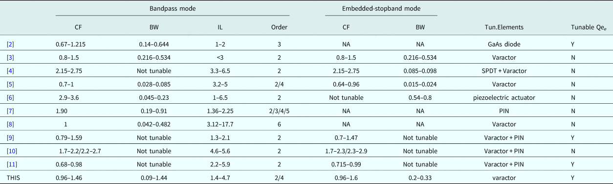
In this paper, a varactor-based reconfigurable filter with center frequency tuning, ultra-wide bandwidth tuning, and bandpass-to-bandpass-with-embedded-stopband reconfiguration is proposed, analyzed, simulated, and measured. The bandpass mode with the center frequency and ultra-wide bandwidth tuning ability are based on the multiple mode resonator and external quality factor tuning structure. The embedded-stopband mode is realized by introducing controllable transmission zeros caused by an additional transmission path. When compared with referenced filters shown above, our proposed filter shows several advantages: the widest bandwidth tuning range among all referenced filters (0.09–1.42 GHz); multi-functionality (tunable CF and BW under both bandpass and bandstop mode), high selectivity (TZs always located near the band), and good insertion loss due to the adoption of the external quality factor tuning structure. Performance comparison is shown in Table 2.
Theoretical analysis
Bandpass mode analysis
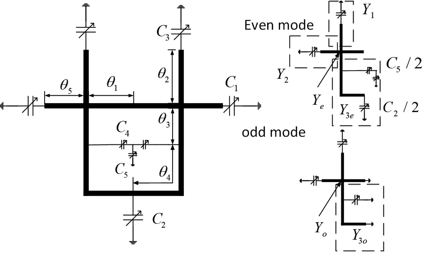
The proposed MMR and its even- and odd-mode equivalent circuit are shown in Fig. 1. Y e and Y o are the input admittance of the even mode and odd mode, respectively. Even-odd mode method can be used to analyze this structure since the structure is symmetrical along its middle plane. The resonant frequencies of the MMR can be obtained by.
 $${\rm Im} (Y_{11}) = 0,$$
 $$Y = \left( {\matrix{ {Y_{11}} & {Y_{12}} \cr {Y_{21}} & {Y_{22}} \cr}} \right) = \left( {\matrix{ {\displaystyle{{Y_e + Y_o} \over 2}} & {\displaystyle{{Y_e-Y_o} \over 2}} \cr {\displaystyle{{Y_e-Y_o} \over 2}} & {\displaystyle{{Y_e + Y_o} \over 2}} \cr}} \right).$$
The simplified structure of the proposed multiple-mode resonator and its even- and odd-mode equivalent structure.

According to equations (1) and (2), the total input admittance can be derived from its even- and odd-mode input admittance. It should be noticed that the characteristic impedance of the microstrip line in this design is a constant value Z, so this parameter is not shown in Fig. 1. The derived even- and odd-mode input admittance equations are as follows:
 $$Y_e = Y \cdot j\tan \theta _1 + Y_1 + Y_2 + Y_{3e},$$
 $$Y_o = -Y \cdot j\cot \theta _1 + Y_1 + Y_2 + Y_{3o},$$
where
 $$Y_1 = Y \cdot \displaystyle{{\,j\omega C_1 + jY\tan \theta _5} \over {Y-\omega C_1\tan \theta _5}},$$
 $$Y_2 = Y \cdot \displaystyle{{\,j\omega C_3 + jY\tan \theta _2} \over {Y-\omega C_3\tan \theta _2}},$$
 $$Y_{3e} = Y \cdot \displaystyle{{Y_L + j\omega Y\tan \theta _3} \over {Y + j\omega Y_L\tan \theta _3}},$$
 $$Y_{3o} = Y \cdot \displaystyle{{2j\omega C_4 + Y\cot \theta _4 + jY\tan \theta _3} \over {Y-(2\omega C_4-jY\cot \theta _4)\tan \theta _3}},$$
 $$Y_L = j\omega (C_4 + \displaystyle{{C_5} \over 2}) + Y \cdot j\displaystyle{{\omega \displaystyle{{C_2} \over 2} + Y\tan \theta _4} \over {Y-\omega \displaystyle{{C_2} \over 2}an\theta _4}}.$$
A rough dimension θ 1 = θ, θ 2 = 1.3θ, θ 3 = 1.2θ, θ 4 = 3.4θ, θ 5 = 1.5θ is given thus we can offer a basic estimation on the multiple modes resonant character by calculating the input admittances. A numerical study based on the above equations can be done to demonstrate the resonant frequency of each mode versus the capacitance value, which can provide a clear guideline for us to understand the MMR's tuning principle. The initial capacitance values are set as C 1 = 1 pF, C 2 = 30 pF, C 3 = 0.1 pF, C 4 = 0.1 pF and C 5 = 1 pF. The characteristic impedance is set to be 120 Ω.
Bandpass resonant modes
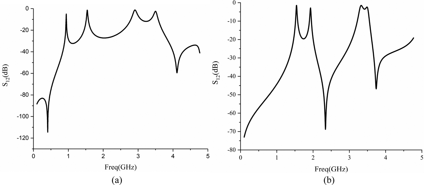
As shown in Fig. 2(a), four resonant modes (defined as: f mode1 < f mode2 < f mode3 < f mode4) can be observed, which form the entire passband for the wide bandwidth bandpass mode. Two transmission zeros are located at both the upper and lower side of the passband to improve the selectivity of the filter. As shown in Fig. 2(b), a transmission zero locates between the lower two resonant modes and upper two transmission modes, which is different from Fig. 2(a). This state is proposed for narrow bandwidth bandpass mode, only the upper two resonant modes will form the narrow passband while the lower two resonant modes can be suppressed by impedance mismatching, therefore a narrow band response can be achieved. The switching between 2 resonant modes and 4 resonant modes are realized by tuning C 1 and C 2. Our goal is to tune these resonant frequencies independently, therefore, the tuning principle should be studied by sweeping the capacitance values and observing the trend of the resonant frequencies.
(a) Four resonant modes state (b) two resonant modes state.

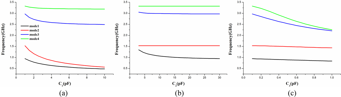
From Fig. 3(a), it can be observed that although all four modes are affected by C 1, the impact on the lower two modes is more significant than the upper two modes. Actually, C 1 is mainly used to tune the external quality factor in this design, which will be illustrated in the section “Tunable External Quality Factor”. Fig. 3(b) shows that C 2 can only change the mode1's frequency and keep other modes stable, which means that this capacitor is a proper choice to tune the lower cut off frequency. Fig. 3(c) shows a similar character to Fig. 3(b) that C 3 can be used to tune the upper cut off frequency. C 4 and C 5 are not shown in this figure because the two capacitors are used in embedded-stopband tuning, which will be demonstrated in the section “Bandpass-with-Embedded-Stopband Mode Analysis”.
Simulated resonant frequencies versus different capacitance values.

Tunable external quality factor
Q e is the external quality factor of an end resonator when it is coupled to port termination and it plays a critical role for tunable filter design. According to traditional microwave theory, the passband performance is related to the quality factor as shown in equation (10).
 $$Q_e = \displaystyle{{\omega _0} \over {\Delta \omega _{3dB}}},$$
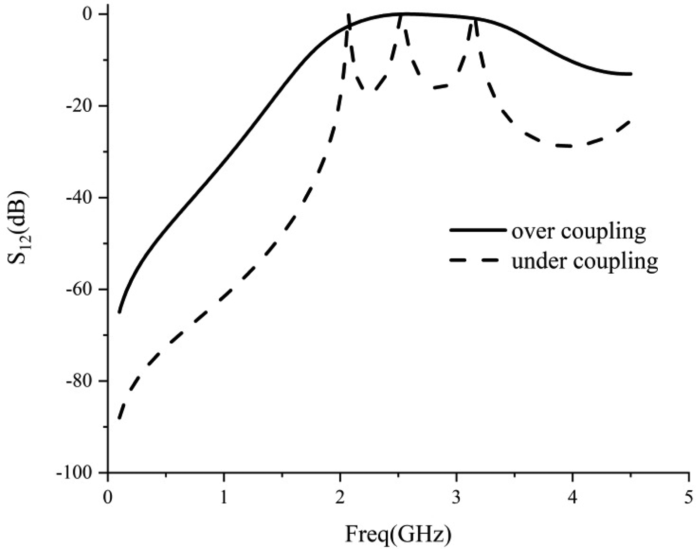
where ω 0 is the angular frequency of the passband and Δω 3dB is the 3 dB bandwidth of the passband. Actually, the essence of this theory is similar to impedance matching theory, if the external quality factor is not suitable for current filtering response, it can also be regarded as impedance mismatching between the feedline and the resonator. We always call this mismatching as over coupling or under coupling when discussing external quality factor. Fig. 4 shows two typical filtering responses with improper external quality factor. As can be observed, under coupling state suffers severely from insertion loss between resonant modes while the attenuation out of band of the over-coupling is terrible.
Filtering response with improper external quality factor.

To achieve an ultra-wide bandwidth tuning range at a fixed center frequency, the external quality factor must change as the bandwidth changes or the passband performance will badly deteriorate.
To tune the external quality factor, a tunable K inverter should be adopted as shown in equation (11). From Fig. 5 we can observe that the tunable K inverter is achieved by a tunable capacitor C 1, which means that C 1 is used in both resonant frequency tuning and external quality factor tuning. Therefore we can conclude that the variable capacitor C 1 is used to control the external coupling value, external quality factor or impedance matching, the three nouns are essentially the same.
 $$Q_e = K^2\displaystyle{1 \over {Z_0}}b_s,$$
where 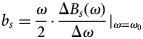 $b_s = \displaystyle{\omega \over 2} \cdot \displaystyle{{\Delta B_s(\omega )} \over {\Delta \omega}} \vert {_{\omega = \omega_0}} $ and
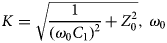 $K = \sqrt {\displaystyle{1 \over {{(\omega _0C_1)}^2}} + Z_0^2}, \,\omega _0$ is the angular frequency of the passband, B s(ω) is the susceptance of MMR and Z 0 is the characteristic impedance.
The tunable K inverter.

Based on the above analysis shown in the section “Bandpass Resonant Modes and Tunable External Quality Factor”, we can give a brief summary on the tuning mechanism for different tuning states under bandpass mode. There are four resonant modes with wide bandwidth and two resonant modes with narrow bandwidth under bandpass mode, as shown in Fig. 3. C 2 and C 3 can be used to tune the lower and upper cutoff frequency of the passband, which can be observed from Fig. 3. C 1 is used to control the external quality factor, from equation (11) it is obvious that the increase of capacitance will lead to the increase of external quality factor.
To tune the center frequency of the passband, C 2 and C 3 should change in the same direction. In this way, the lower cutoff frequency (controlled by C 2) and upper cutoff frequency (controlled by C 3) will move to the different center frequency direction simultaneously with a stable bandwidth. C 1 also need to be slightly tuned to fit different external quality factors under different center frequency.
To tune the bandwidth of the passband, C 2 and C 3 should change in the opposite direction. The lower cutoff frequency(controlled by C 2) and upper cutoff frequency(controlled by C 3) will move to the opposite direction accordingly. In this way, the bandwidth can be tuned under a fixed center frequency. To achieve a wide bandwidth tuning range, C 1 needs to be adjusted as bandwidth changes. Otherwise, the passband performance will badly deteriorate for the improper external quality factor.
Bandpass-with-embedded-stopband mode analysis
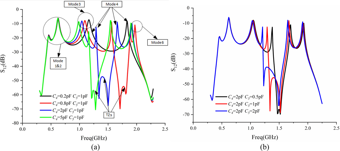
The bandpass-with-embedded-stopband mode can be obtained by controlling C 4 and C 5, which will introduce another two resonant modes (defined as mode5 and mode6) and another two transmission zeros (defined as TZ1 and TZ2). The six resonant modes form a constant passband and two transmission zeros form the embedded-stopband. The two transmission zeros are induced by the T capacitor junction consisting of C 4 and C 5. The reason of their occurrence is that there must be a 180° phase difference between the main signal transmission path and the T capacitor junction signal transmission path at some certain frequencies and it is obvious that a 180° phase difference will cause a transmission. Once the frequencies with 180° phase differences can be controlled by C 4 and C 5, the center frequency and bandwidth of the embedded-stopband can, therefore, be controlled. The T capacitor junction is also symmetrical along the middle plane, thus the odd- and even-mode method is still useful in this analysis. Based on the even-odd mode analysis, C 4 can control two transmission zeros induced by both even mode and odd mode from the capacitor junction, C 5 can only control one transmission zero induced by only even mode from the capacitor junction. In this way, the center frequency and bandwidth of the embedded-stopband can be tuned independently.
As shown in Fig. 6, when C 4 and C 5 are relative low, mode5 and mode6 locate far away from mode1 to mode4. This is the bandpass mode as black line shows. As C 4 and C 5 become larger, mode5 and mode6 will move closer to mode4 and two TZs will appear between mode4 and mode5,6(f mode1 < f mode2 < f mode3 < f mode4 < f TZ1 < f TZ2 < f mode5 < f mode6), as shown in Fig. 6(a). Under this state, the lower and upper cutoff frequency of the passband is mode1 and mode6, respectively, which is different from bandpass mode. As shown in Fig. 6(b), keeping C 4 at a fixed value while tuning C 5, only one transmission zero moves. This situation accords with our previous expectation in the first paragraph. The center frequency and bandwidth of the stopband can be tuned independently because of the two controllable TZs.
(a) Stopband center frequency tuning (b) stopband bandwidth tuning.

In this section, we also give a brief summary on the tuning mechanism for different tuning states under bandpass-with-embedded-stopband mode. The passband is formed by totally six modes while two transmission zeros are embedded into the passband as “embedded-stopband.”
The center frequency of the embedded-stopband can be tuned by simply controlling C 4 because two transmission zeros all affected by C 4. C 5 can be used to tune the bandwidth of the embedded-stopband because only one transmission zero is affected by this capacitor. During this tuning process, the passband maintains constant.
Design technique and tuning logic
Although this design is mainly accomplished by iterative optimization, it is still necessary to provide design steps for readers who are interested in redo this work at a particular working frequency. We need to build a rough structure first and observe the location of resonant modes and transmission zeros, and then optimize the structure's dimension towards our desired frequency based on the varactors' capacitance tuning range. Several design techniques are listed as follows for different tuning states:
(1) For the determination of wide passband center frequency: The center frequency of the passband in this state is determined by all four resonant modes. If the length of microstrip line L 1 and L 5 is increased (as shown in Fig. 7) or the line width W is decreased, all four modes will move to the lower side. In this way the center frequency of the wide passband can be adjusted to a particular value.
Fig. 7.Two-stage cascaded multiple-mode resonator for higher order filter design.

(2) For the determination of narrow passband center frequency tuning range: The center frequency of the passband in this state is determined by the upper two resonant modes. If L 2 is increased then the center frequency tuning range of the narrow passband will move to the lower side.
(3) For the determination of bandwidth tuning range: The attainable widest bandwidth is determined by the gap between the lower two modes (can be adjusted by L 6) and upper two modes, but it is also limited by the external quality factor value.
(4) For the determination of embedded-stopband center frequency and bandwidth: the two transmission zeros, which forms the stopband, always located near the four resonant mode when C 4 and C 5 is relative low. The only impact factor on the tuning range of embedded-stopband is the varactors' capacitance tuning range and the T varactor junction's location.

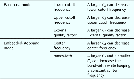
A brief tuning logic of the bandpass-to-bandpass-with-embedded-stopband filter is provided, as shown in Table 1.
Tuning logic of the proposed filter

Higher order filter design
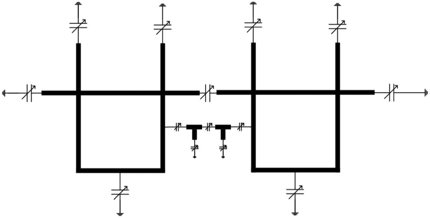
This design can be expanded to higher-order filters by cascading several replicas of the proposed multiple-mode resonator shown in Fig. 1 with small modifications.
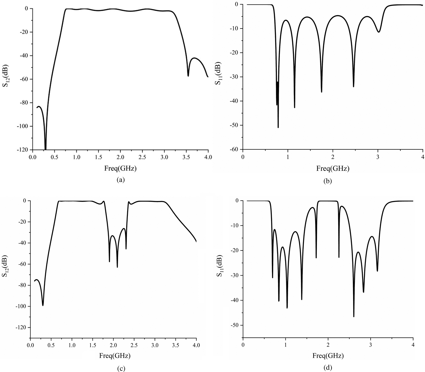
As an example, Fig. 7 shows a two-stage cascaded multiple-mode resonator for higher order filter design. Two multiple mode resonators are cascaded in series as “two stage” which can provide a higher order passband response. The previous T capacitor junction is also modified by adding a new capacitor-loaded stub, which can provide a higher order stopband response. Fig. 8 shows the simulated fully matched bandpass and bandpass-with-embedded-stopband response of this proposed higher-order design. From Figs 8(a) and (b), a wider passband can be observed from the passband response, which indicates that more resonant modes are included in this response. From Figs8(c) and (d), a three-stage stopband can be observed from the bandpass-with-embedded-stopband response, which suits the expectation of modified capacitor junction.
Simulated response of higher order multiple-mode resonator for bandpass response and bandpass-with-embedded-stopband response.

Measured results and discussion
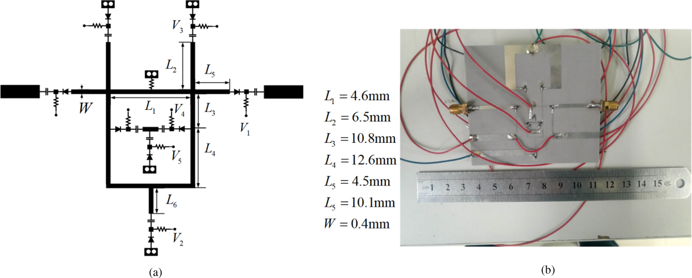
The layout, optimized physical dimensions and photographs of the proposed fully reconfigurable filter are shown in Fig. 9. The proposed structure is fabricated on the F4B-2 substrate (thickness: 0.8 mm, relative permittivity: 2.65, dielectric loss tangent: 0.01). V 1, V 4, and V 5 are SMV1281-079LF, V 2 is SMV1248-079LF, and V 3 is SMV1405-079LF. The 50 pF Murata capacitors are used as DC blocks and 10 kΩ resistors are used as RF chokes. Co-simulations are accomplished by EM commercial software HFSS and ADS. The simulation steps are as follows: (1) build the layout of the proposed filter in HFSS and set the lumped port at all locations where lumped elements are loaded. (2) Export the solved data into SNP file from HFSS (N is the number of lumped port). (3) Build varactor diode model in ADS, related information can be found in datasheets. (4) Select “data item” – “SNP” component in ADS and import SNP file into it, then connect each port with their corresponding varactors, RF chokes or DC blocks then simulate it.
The layout, optimized physical dimensions, and photographs of the proposed filter.

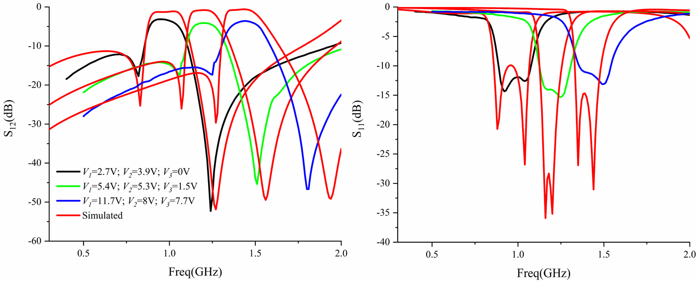
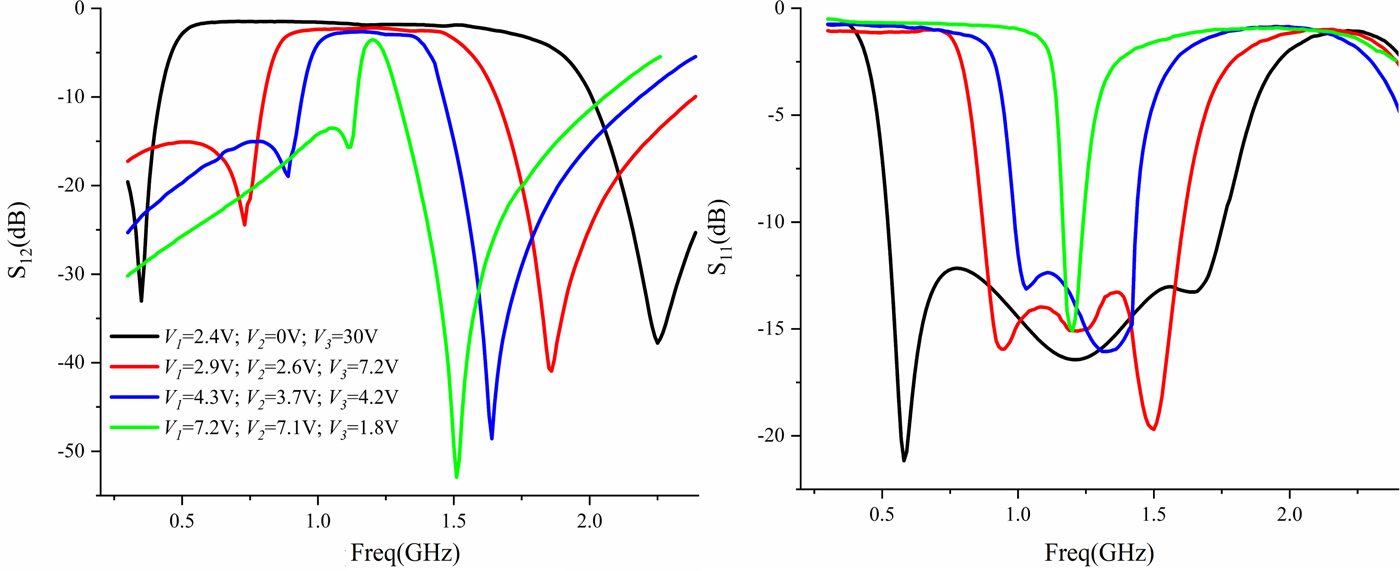
Figures 10 and 11 show the measured and simulated S-parameter under bandpass mode. The 3-dB bandwidth can be tuned from 0.09 to 1.41 GHz for a fixed center frequency 1.22 GHz. The center frequency varies from 0.96 to 1.45 GHz. The insertion loss is 1.4–4.7 dB for all tuning states.
Simulated and measured S 11 and S 12 for center frequency tuning under bandpass mode. V 4 and V 5 are fixed at 30 V for all states. Red lines are the corresponding simulated results.

Measured S 11 and S 12 for bandwidth tuning under bandpass mode. V 4 and V 5 are fixed at 30 V for all states.

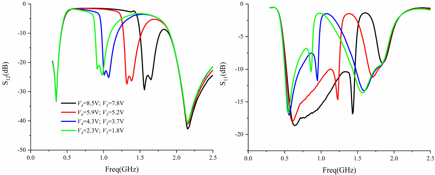
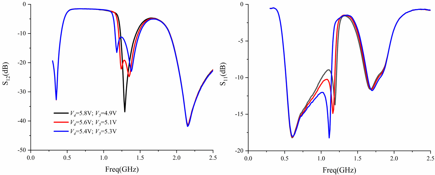
Figures 12 and 13 show the measured S-parameter under bandpass-with-embedded-stopband mode. The 3-dB bandwidth can be tuned from 0.2 to 0.33 GHz. The center frequency varies from 0.94 to 1.61 GHz. The attenuation level is >10 dB for all tuning states.
Measured S 11 and S 12 for center frequency tuning under bandpass-with-embedded-stopband mode. V 1, V 2, and V 3 are fixed at 2.7, 0 and 30 V for all states, respectively.

Measured S 11 and S 12 for bandwidth tuning under bandpass-with-embedded-stopband mode. V 1, V 2, and V 3 are fixed at 2.7, 0, and 30 V for all states, respectively.

Note that despite simulations are only shown for some tuned states for clarity, a similar agreement for all measured results is obtained.
Table 2 shows the performance comparison between the proposed and referenced filters. Three advantages can be observed in Table 2: (1) the proposed fully reconfigurable filter has the widest passband bandwidth tuning range among all referenced filters. (2) The proposed filter also have an excellent insertion loss performance due to the adoption of the external quality factor tuning structure, although Ref [Reference Mao, Choi, Tam, Che and Xue2] and [Reference Psychogiou, Gómez-García and Peroulis6] shows a better performance in the IL performance, the price of their tuning components (GaAs diode and piezoelectric actuator) is much higher than varactors used in this design. (3) A complete multi-functionality can be observed from this design.
Performance comparison between proposed and referenced filters

Conclusion
A bandpass-to-bandpass-with-embedded-stopband fully reconfigurable filter with center frequency and bandwidth tuning ability is presented in this paper. Several advantages, for example, an ultra-wide bandwidth tuning range and multi-functionality are achieved in this design based on multiple mode resonator and external quality factor tuning structure. Based on the analysis, the operational principle is well investigated thus filter geometry and tunable elements can be determined according to the filter specification. Excellent performance can be found from the comparison table. The filter is expected to find applications in carrier aggregation and cognitive radios.
 Bozhang Lan was born in Shaanxi Province, China, in 1992. He received the B.S. degree in Electronic Science and Technology from HeFei University of Technology and M.S. in Electromagnetic Field and Microwave Technology from the School of Electronic and Information, Northwestern Polytechnical University. He is currently pursuing Ph.D. degree in Northwestern Polytechnical University. His research interests include microwave passive components and their reconfigurable type.
 Yan Qu was born in Xinjiang Province, China, in 1987. He received the B.S. degree in Electronic and Information Engineering and Ph.D. in Electronic Science and Technology from the School of Electronic and Information, Northwestern Polytechnical University, 2010 and 2017. He is now working in China Academy of Space Technology (Xi'an) as an antenna engineer. His research interests include phased array antenna design and synthesis.
 Chenjiang Guo was born in Shannxi Province, China, in 1963. He is CIE Senior Member, Antenna Society Committee Member. He received the MSc. BSc., and Ph.D. in School of Electronics and Information, Northwestern Polytechnical University in Xi'an city, China, in 1984, 1987, and 2007, respectively. He is a professor in School of Electronics and Information NWPU. He has published more than 140 research papers. He research interests include EMI/EMC, the antenna theory and design, and the microwave circuit design.
 Jun Ding was born in Shannxi Province, China, in 1964. She received the MSc. BSc., and Ph.D. in School of Electronics and Information, Northwestern Polytechnical University in Xi'an city, China, in 1986, 1989, and 2005, respectively. She is a professor in School of Electronics and Information NWPU. She has published more than 100 research papers. Her research interests include Electromagnetic Metamaterials, the antenna theory and design, and the microwave circuit design.