

DISCUSSION POINTS
• How to predict user behavior (e.g., willingness to upgrade in a few years, willingness to perform simple repairs of high-tech products) for a disruptive product concept not yet introduced to the market (e.g., modular smartphones)?
• How to define policy requirements setting the right incentives for circular design, considering trade-offs between different design strategies, such as design for reparability and durability?
• In case, modular product concepts are introduced in the market at large, which new business models will follow?
Introduction
Most of the environmental life cycle impacts of current mobile devices, such as smartphones, tablets, and laptops are related to high-tech manufacturing processes, such as semiconductor manufacturing and printed circuit board processing. Raw materials acquisition, although being characterized by a huge multitude of used elements, is of minor relevancy. Material recycling consequently can yield “environmental credits” only to a limited extent. Lifetime extension of functional devices and parts, therefore, is the most promising strategy to reduce the overall environmental footprint of using mobile information and communication technology (ICT) devices.
On the example of circular design trends of smartphones, apparent material trends will be analyzed in this research.
Sustainability motivation for modular smartphone design
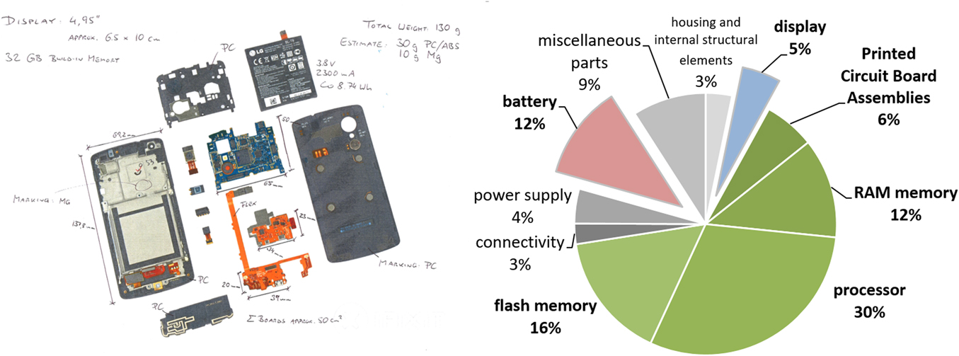
Modularity of products is a design trend, which is supposed to facilitate reparability, recyclability, and/or upgradeability. The rationale from a life cycle perspective is the fact that some well-defined parts of smartphones are typical weak spots of any design and fail most frequently. These are typically displays due to accidental drops and at a certain point of time the battery which faces a reduced charging capacity due to aging effects. The carbon footprint, i.e., the greenhouse gas emissions, for producing displays and batteries is small compared with the main electronics, such as RAM and flash memory, the smartphone processor, and printed circuit board assemblies in general, see Fig. 1. Under these conditions, the lifetime of display and battery should not limit the lifetime of those other parts produced with a much higher environmental impact.
Carbon footprint of smartphone parts.

The solution is either an extremely durable display design and a battery lifetime, which does not make the battery anymore the lifetime-limiting component, or a product design, which enables easy replacement of at least the display and the battery. A modular design is the corresponding approach. However, modularity requires some design changes. In case of mobile ICT, such as smartphones or tablet computers, the most evident design change is the need for connectors to provide mechanical and electrical contact between individual modules.
Modularity approaches
Modularity comes in various shades, depending on the intended or anticipated use patterns or business model related to modularity. Some modular products are available in the market, others are still in a conceptual phase. This variety of modularity approaches is related to different value propositions, thus leading also to a broader range of modularity archetypes.
Among smartphones, the modularity is classified as below, which is an extended classification based on a modularity typology first published in 2016:Reference Schischke, Proske, Nissen and Lang1
Material modularity
Some materials such as covers and batteries can be easily separated. This is a rather conventional type of smartphone modularity, which was common until a few years ago when high resistance against dust and humidity ingress (stated as IP, ingress protection classes) was not yet the dominating feature of smartphones. Product examples are the first Fairphone, Samsungs’ Galaxy S5 (which actually featured IP 672), and many more.
Internal modularity for serviceability
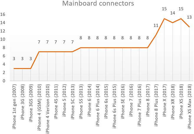
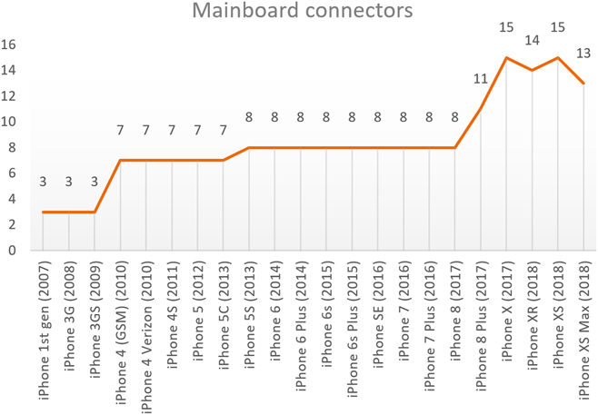
Several large smartphone manufacturers recently increased the level of internal modularity, which actually is accessible only to professional staff. One driver for such internal modularity is apparently the flexibility in the design, including advantages to change individual components and module designs in case of parts being discontinued. Another obvious driver is the improved serviceability: In case of a malfunction, individual modules can be replaced. Apple increased over time the number of connectors on the main logic board, which indicates this trend toward increased internal modularity (see Fig. 2): Recent iPhone generations feature 13–15 connectors on the mainboard, whereas first iPhones contained logic boards with only three connectors. Similar trends are observed among other leading manufacturers.
Amount of connectors on logic boards of iPhones.
Repair modularity on board level
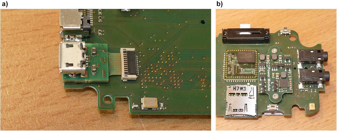
Individual functional building blocks are placed on the mainboard and are connected reversibly. Manessis et al.Reference Manessis, Schischke, Pawlikowski, Krivec, Schulz, Podhradsky, Aschenbrenner, Schneider-Ramelow, Ostmann and Lang3 developed such a concept for a digital voice recorder: The basic concept involves miniaturized modules, making use of embedding technology to reach small form factors. The approach is similar to the use of processor sockets in personal computers—now in a miniaturized variant. Positive theoretical effects include feasibility of board level repairs and board level upgrades, component obsolescence resilience, redesign is simplified, and a less complex backbone board. This concept is not yet known for smartphones but theoretically transferrable (Fig. 3).
Modules with embedded components on mainboard prototype: (a) USB module and (b) digital signal processor and power modules (Ref. Reference Manessis, Schischke, Pawlikowski, Krivec, Schulz, Podhradsky, Aschenbrenner, Schneider-Ramelow, Ostmann and Lang3, copyright G. Podhradsky/Speech Processing Solutions, with permission).

Platform modularity
The product can be configured for a range of individual specifications but requires a basic technical knowledge. This is rather a concept for hackers or to test product ideas. This concept has been introduced to the market in 2015 under the name RePhone.
Do-it-yourself repair modularity
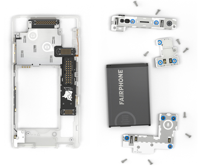
A modular design can facilitate do-it-yourself (DIY) repairs by enabling access to modules with simple tools, if tools are required at all, and easily identifiable and exchangeable functional blocks. An example is the Fairphone 2,Reference Hebert4 which does not require any tools to get access to the battery and the display and only a screw driver to separate four electronic modules. The environmental advantage is the fact that the barrier for repairs is extremely low as costs of professional services do not apply and only shipping of individual modules is required to get a repair done, not shipping the whole device back and forth to a servicing center. With this, it is more likely that repairs will actually happen in case of malfunctions. The Fairphone 2 was introduced to the market in European countries in 2015 (Fig. 4).
Modular concept of the Fairphone 2 (Copyright Fairphone B.V., CC BY-SA, with permission).

Upgrade modularity
Replacing after a certain time of use a module with a module of better performance allows to keep pace with the growing user expectations over time. A memory upgrade would be such kind of feature. In case of the Fairphone 2, a better camera module has been released some time after initial product release. This upgrade concept requires a long-term compatibility of interfaces, including software. Besides the Fairphone camera example and the occasionally found feature to extend memory with an SD memory card, no such upgrade modularity is yet found in the smartphone market.
Mix and match modularity
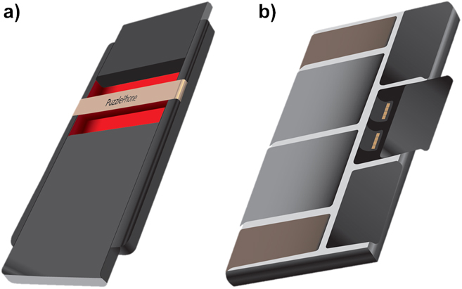
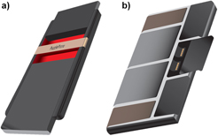
Modules are available in different variants and are fully compatible with each other. The phone functionality, including core functions, is realized by combining several modules. This involves a joint backbone and/or standardized module interfaces. This concept includes upgradeability, repair modularity, and ultimately hot-swapping is an option. Examples are not yet on the market and include the PuzzlePhone by Circular DevicesReference Jokinen5 and the Google ARA project,6–Reference Knaian and Yeh8 which was terminated in 2016 (Fig. 5).
Modular concept of (a) the PuzzlePhone and (b) the Google Project ARA.

Add-on modularity
For some phones, compatible accessories are available, which add functionality to the basic phone features. This was a concept back in the past when miniaturization had not yet reached today’s levels, e.g., first cameras were introduced to the mobile phone market (see the 2002 phone with plug-in camera depicted in Fig. 6). Today, the most prominent example is the Moto Mods: a video projector module, a sophisticated digital camera module, a loudspeaker module, and an additional power module are available from Motorola and compatible with the core smartphone, but the interface specification is also available to third parties to prototype different compatible modules.
Mobile phone with external camera (Siemens S55, market introduction: 2002).

Repurposing and system modularity
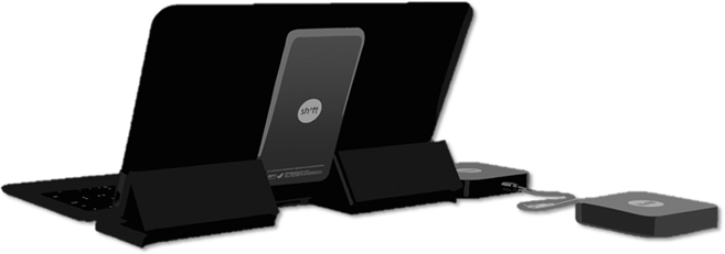
Even before the release of the first PuzzlePhone, the inventors already gave it some thought what might happen with the main electronic module after first life: The idea is to connect several of these electronic modules as a mini-computer (“PuzzleCluster”).Reference Santacreu9 In a slightly different approach, company SHIFT plans to make their smartphone compatible with a display and keyboard.Reference Schischke, Nissen and Lang10 The phone then represents the computing core of a tablet or small desktop computer (Fig. 7).
Concept of a smartphone acting as a main computing unit for a tablet and computer (SHIFTmu bundle).

Table 1 summarizes the different identified types of smartphone modularity and lists related environment product aspects.
Modularity classification.

Repair, reuse, and upgrade assessment of modularity concepts
Modularity as a design approach to enhance sustainability of ICT usage currently finds its policy counterpart in the European Union’s regulation on ecodesign for a broad range of products: The European eco-design legislation allows for setting product-related material efficiency criteria and minimum standards.11 Several related standards are under development by the European standardization bodies CEN (European Committee for Standardization) and CENELEC (European Committee for Electrotechnical Standardization). One of these standards is explicitly on defining methods for the assessment of the ability to repair, reuse, and upgrade energy-related products (prEN 4555412), others are, inter alia, on durability,13 remanufacturability,14 and recyclability.15 As modularity concepts frequently target at enhanced reparability, (module) reuse, and upgradeability, a comparison of identified design features with the upcoming scoring criteria under prEN 45554 helps to figure out, whether modularity will be assessed favorably under a potential future product regulation for smartphones. It is important to keep in mind that modularity will also have an effect on product assessments under the other material efficiency standards: Modularity is likely to have an effect on durability, which includes, in the sense of prEN 45552, aging, fatigue, and wear-out due to environmental and operating conditions.13 Additional interfaces for modularity and a good ingress protection being in conflict with easy access to components are indicators that durability of modular smartphones might be worse than for conventional designs, but a detailed scientific assessment of this correlation remains to be done. Recyclability is rather improved by modular design, as has been shown for the Fairphone 2 in a comprehensive recyclability assessment.Reference van Schaik and Reuter16 Similarly, a positive correlation between the criteria on remanufacturability according to prEN 45553 and modular designs, which enable exchange of functional modules, can be expected, but verification of this assumption is pending.
The repair, reuse, and upgrade (RRU) criteria listed in Table 2 are those defined by prEN 45554 and related to the product design as such. There are further support-related criteria, which are of a management and organizational nature, such as availability of spare parts, types and availability of information, return options, data management, and password and factory reset for reuse. As these are not directly related to a product design, they are not included in the screening assessment in Table 2. A key term for the RRU scoring is “priority parts,” which are those with a high average occurrence of failure, containing personal data, and those subject to rapid technological changes or changes in user profiles.12 With this generic definition, there is no unambiguous clarity what are priority parts of smartphones. Cordella et al.Reference Cordella, Alfieri and Sanfélix17 suggest a rather short list of priority parts for smartphones:
(i) Screen
(ii) Back cover
(iii) Battery
(iv) Operating system
RRU screening of modularity types.

Matrix legend: o: no relevant correlation; +: favorable scoring; ++: very favorable scoring.
Given the “rapid technological changes” in storage density and also due to the personal data issue, memory might also qualify as priority part (for reuse and upgrade) and theoretically also the processor (CPU), but upgrading a CPU is extremely complex as this has effects on the whole system. It might be arguable that the continuing innovations in imaging technology and settings also make cameras a priority part for smartphones. With this range of priority parts in mind, the RRU screening of the modularity types in Table 2 provides a first screening, if a positive correlation between RRU criteria and the modularity types identified in our research exists. Disassembly depth represents the number of process steps needed to remove a broken part from a device; fasteners and connectors are distinguished for reusability, removability, and non-removability; tools are categorized depending on how common these are; the working environment criterion refers to specific precautions or processing conditions for a successful repair, reuse, or upgrade process, and the skill level takes into account if laymen or manufacturers or anybody in between these two extremes will be able to perform a required RRU process.
Internal modularity and repair modularity on board level are not likely to reduce the number of disassembly steps, resulting in a neutral assessment. However, non-permanent fasteners and connectors in internal modules and on board level are favorable, and the assessment in the related column for internal modularity and repair modularity on the board level is favorable—if any of the relevant internal modules are defined as priority parts in the end. DIY repair and mix and match modularity scores are high for all criteria, but again only if the priority parts are individual modules. The definition of the back cover as a priority part in case of the fragmented designs of the PuzzlePhone and the Google ARA concepts is problematic as the modules each feature an external surface. Add-on modularity typically targets at modules, which are features that are not essential for the core function of the smartphone (see list of Moto Mods provided above, except for the battery extension), and as such, this modularity concept is only weakly linked to the proposed RRU criteria. Repurposing and system modularity seems not to be linked to the existing RRU criteria (applied to defined priority parts) at all, which unveils a weakness of the proposed material efficiency assessment framework: Positive side effects through repurposing of the whole device are not properly addressed although the environmental potential is significant, if other devices can be replaced by a reused device or a device serving multiple other computing purposes.
Now, as the correlation between the various modularity concepts and ecodesign standards has been clarified, it is important to analyze the technical measures to implement modularity.
Connector designs and specifications
Connectors are a key element for any design consisting of distinct building blocks.
Among the connectors, electrical (power and data) and mechanical connectors have to be differentiated. Frequently, both functions, electrical and mechanical contact, are facilitated by the same connector part.
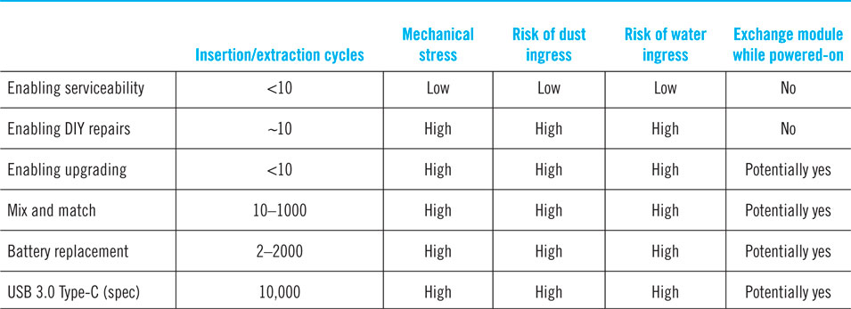
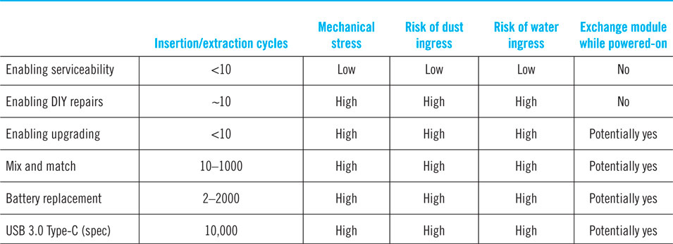
Connectors per se are a weak spot and due care has to be given to reliability and robustness of these. Durability requirements for connectors depend on the actual intended use case. A modularity targeting at serviceability means that it is unlikely that a given connector sees more than a few mating–unmating cycles. Likely a given module will only be connected and disconnected once or twice throughout the lifetime if at all. In case the design is supposed to facilitate DIY repairs, the connector is likely to see more stress: The barrier to undertake a repair is lowest, if this can be done by laymen. As laymen are less experienced than professional repair staff, modules might be inserted repeatedly for a given repair to make it work properly. Furthermore, handling will be less gentle and mechanical stress on connector parts is likely to be higher. Upgrading is likely not to happen very often and the number of insertion/extraction cycles is likely to stay below 10. Designs supporting a highly flexible configuration (mix and match modularity) might indeed see a change in modules on a daily basis as a user might want to use different functions embedded in different modules throughout the week. For such a scenario, insertion/extraction cycles might be in the range of 1000. For an easily exchangeable battery, the number of related cycles might be even higher as a user might own two batteries, one to be used in the phone, the other one being charged in parallel. For a heavy user, this might mean exchanging batteries twice a day, 2000 times over a 3 years lifetime. For comparison, the durability rating of USB Type-C connectors shall be 10,000 insertion/extraction cycles according to the harmonized specification.18 Except for enhanced serviceability, which might be realized in a tightly sealed device, connectors for all other modularity purposes are typically subject to a high risk of dust and water ingress. Water ingress is related to a risk of corroding surfaces, which can hamper functionality of the connectors. Depending on the likely use scenario, connectors might be disconnected while under power. For high power applications, this makes a huge difference due to arc effects, but less so for low power applications, such as mobile ICT devices. Nevertheless, this aspect should be taken into account. In the cases of upgrading, mix and match modularity, and battery replacement, the connectors are likely to be connected and disconnected when power is on (“hot-swapping”) (Table 3).
Connector durability requirements.
Types of typical connectors for various kinds of smartphone modules are as follows:
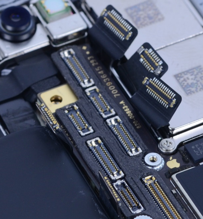
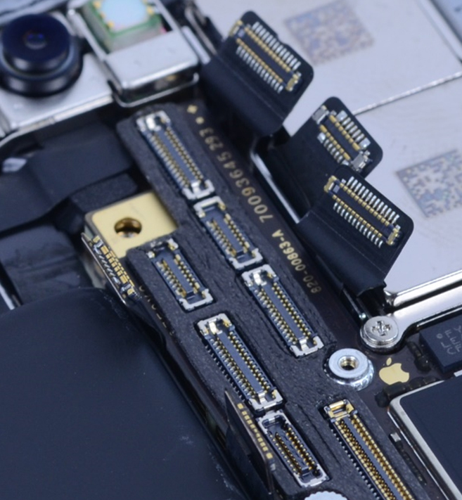
Standard board-to-board connectors in smartphones and many other small devices are mezzanine strip connectors (Fig. 8). Due to the tiny dimensions, these connectors are of limited robustness and will withstand only a limited number of mating and unmating cycles. With a small footprint, these connectors provide a high interconnect density and typically connect from the logic board through a flex board to a remotely located subassembly of a given functionality.
Mezzanine strip connectors in current iPhone designs.
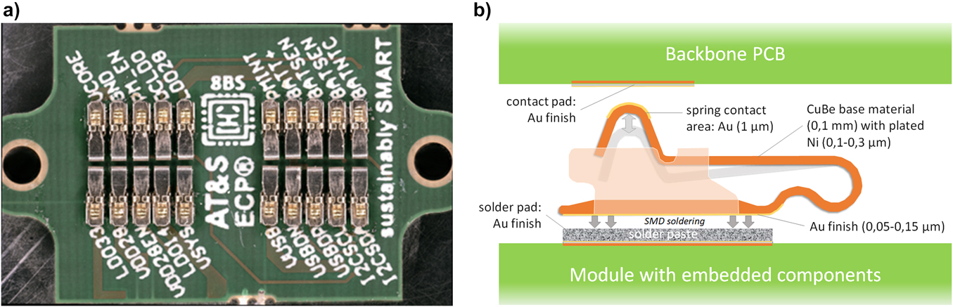
Non-permanent connectors between rigid modules and a backbone board (“repair modularity on board level”) could be spring contacts for the electrical contact (Fig. 9). A demonstrator developed by Speech, AT&S, and Fraunhofer IZM employs screws for the mechanical fixation of the depicted module.Reference Schischke, Manessis, Pawlikowski, Kupka, Krivec, Pamminger, Glaser, Podhradsky, Nissen, Schneider-Ramelow and Lang19
(a) Bottom side view of the spring array on a power module (copyright T. Krivec/AT&S, with permission) and (b) schematic drawing of a spring assembly.

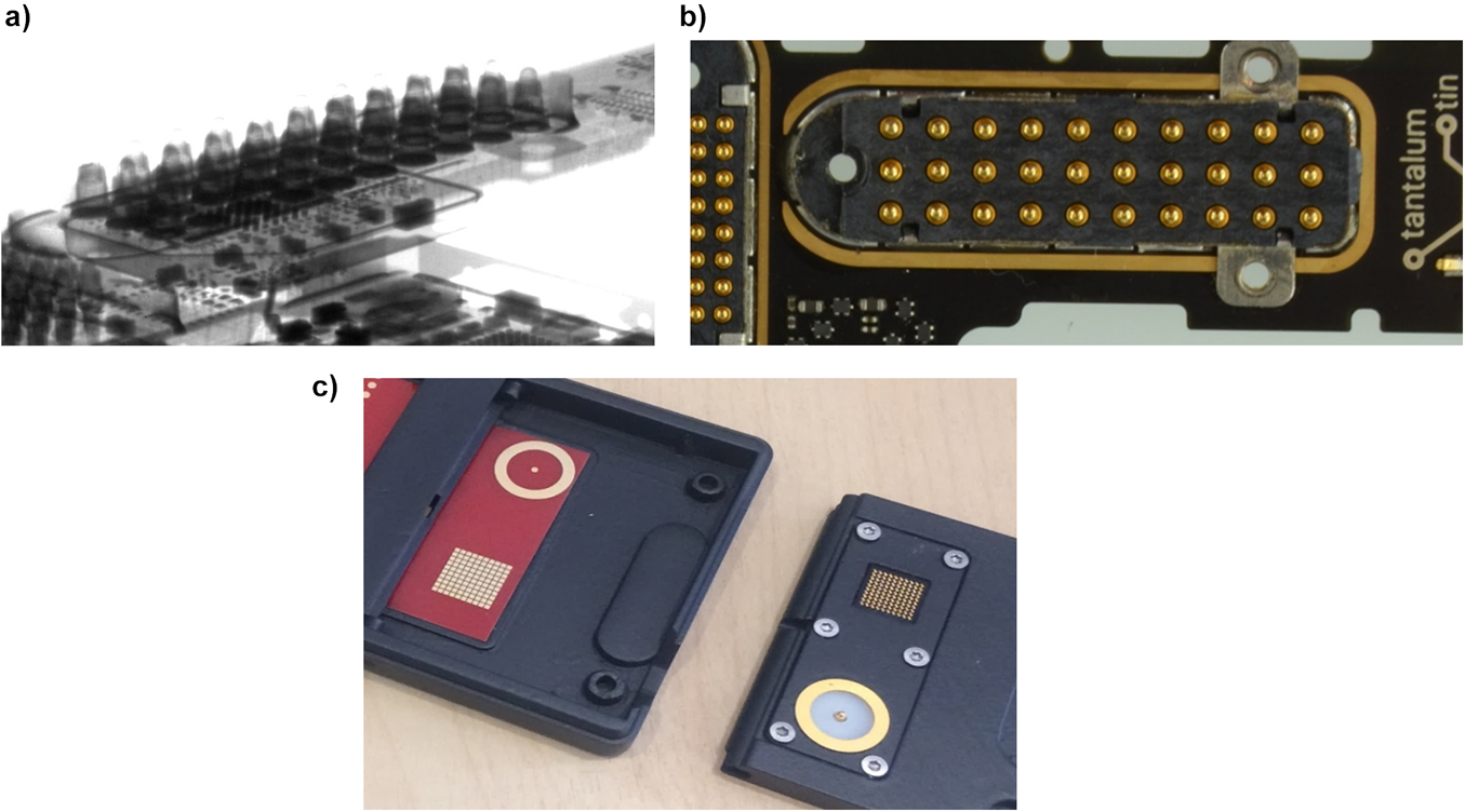
Typical connectors that withstand frequent mating and unmating cycles are spring-loaded pins, frequently also called pogo pins (Fig. 10). These are typically used in printed circuit board electrical test equipment, but also docking stations, and are candidates for DIY repair modularity and mix and match modularity, where modules might be replaced more frequently and handling by laymen is less gentle. It should, however, be noted that in case of test equipment contact is made several 10,000 times, which is far beyond the requirement for mobile ICT devices, and already indicates that these might be overdesigned for smartphone applications.
Spring-loaded pins in modular smartphones: (a) X-ray oblique view, (b) top view of Fairphone 2 board-to-display connector, and (c) prototype PuzzlePhone coaxial antenna connector (copyright A. Santacreu/Circular Devices, with permission).

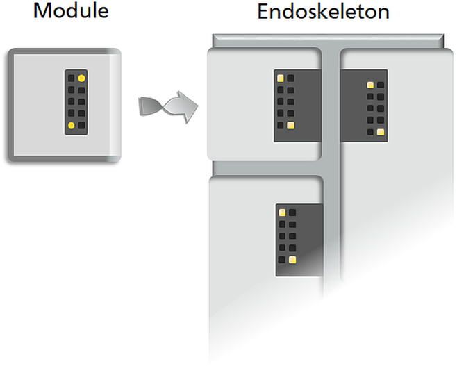
The first design iteration of the Google ARA project specified gold-coated spring-loaded pins for the power pads on the modules and corresponding gold coated pads on the endoskeleton. The data pads were supposed to be copper6 (Fig. 11). The second design iteration specified inductive coils for data and power transmission.7 In both designs, mechanical fixation of modules is made through magnets.
Google ARA first design iteration.

These are some of the connector designs found in current products, prototypes, or concept studies, but this is not a conclusive list of technical solutions, in particular, for mechanical connectors many more options are thinkable, ranging from simple clip connectors to Velcro-type solutions or debondable adhesives.
Modularity materials
Modularity of mobile ICT devices relates to additional connectors—as described above—housings, shielding, and substrates. Analyzing technologies for modularity leads to a group of “modularity materials,” which are essential for such circular design approaches but at the same time are among those materials with a large environmental footprint or limited recyclability. The following analysis correlates the technical requirements of modularity-enabling components with the use of specific materials.
Depending on the nature and use scenario of a connector reliability, robustness, wear resistance, and non-reactive surfaces are required. Gold is the material of choice for such interfaces. In recent years, the amount of gold used in electronics decreased, now with emerging modularity among ICT devices, gold as a material with a high environmental impact might return into devices in larger amounts.
According to manufacturer’s specifications, gold-coated contacts, which are subject to mechanical stress, are frequently specified with a layer thickness of 1 µm,20 but also down to 0.1–0.2 µm.21 A mezzanine board-to-board connector is plated with 0.2 µm gold at mating surfaces and specified for 30 mating cycles,22 which is sufficient for repair modularity. Gold layer thicknesses for plug connectors differentiated per application according to VinarickyReference Vinaricky and Vinaricky23 are listed in Table 4.
Hard gold layer thickness of plug connectors depending on application.Reference Vinaricky and Vinaricky23

Most smartphone modularity concepts match with the category “standard environment,” and as such, a layer thickness of 1 µm seems to be overdesigned.
Flash gold layer thickness for high-quality surface finishes on pads for soldering is 0.05–0.15 µm, see different parts of the spring illustrated in Fig. 10(b). The tip of a spring-loaded pin has to be plated with a similar gold layer thickness as other contacts. Contact pads are typically copper with a nickel coating and gold finish. An alternative low-cost material compared with gold for connectors in consumer applications is tin. Due to its low hardness, tin finishes are of very limited wear resistance and are only applicable for less than 20 mating cycles.Reference Heber and Vinaricky24 Among the investigated modularity concepts for smartphone, no use of tin finishes has been identified.
The material of choice for particularly stress-resistant springs, either in spring-loaded pins or as spring contacts, but also for ring springs25 is copper beryllium alloy (CuBe2 and CuBe1,7, thus the content of Be is actually rather low) due to outstanding mechanical properties and good conductivity.Reference Vinaricky, Buresch and Vinaricky26 For those modularity applications with less mating cycles, and where, e.g., a spring is not supposed to be subject to continuous stress (e.g., vibration) under normal use conditions, it might not be required to use CuBe as base material, and brass (CuZn alloys), which is in widespread use for connectors, could be a viable alternative. Other alloys used as contact material base in connectors are CuNi3SiMg, CuNi9Sn2, and CuCo0.5Be, the latter with a reduced Be content of 0.15–0.5 mass% and a rather high bending fatigue strength of 280 MPa.Reference Vinaricky, Buresch and Vinaricky26
For reversible mechanical fasteners, a broader range of technologies might be used, frequently magnets are proposed as a simple and robust option. To achieve strong magnetic forces, rare earth elements are used, mainly neodymium or other critical raw materials, such as cobalt. The magnet assembly of the Google ARA specification defined for the use on the endoskeleton side NdFeB permanent magnets and Alnico magnets with a coil to switch on/off magnetic force of the endoskeleton. Alnico alloys of magnets are typically of a composition 8–12% Al, 15–26% Ni, 5–24% Co, up to 6% Cu, up to 1% Ti, and balance: Fe. On the module side, Hiperco-50 alloy is specified as magnetic material, containing 48.75% Co.Reference Knaian and Yeh8
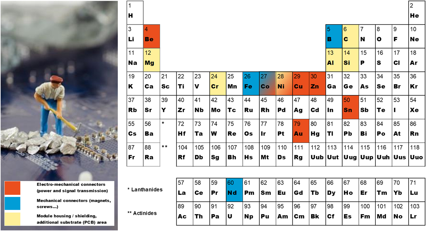
Figure 12 summarizes those elements that are required for modularity features.
Modularity elements.

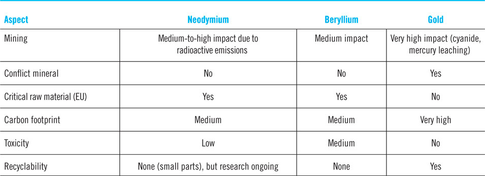
The environmental impacts of the aforementioned dominating elements in modularity components are manifold and multidimensional: Environmental impacts include resource consumption such as, circularity of materials, i.e., how well these can be extracted and recovered from a waste stream, emissions of human toxic and eco-toxic substances and greenhouse gases throughout all phases of the life cycle, and in a broader sustainability sense also the use of minerals from conflict regions, and raw materials considered as “critical” for an economy.
As an example for limited circularity, rare earth elements such as Nd from module magnets are not yet properly recovered from waste electrical and electronics equipment,Reference Reuter and van Schaik27 thus modularity might even contradict better recyclability.
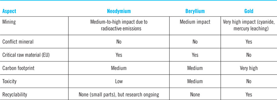
Neodymium compounds are of low-to-moderate toxicity, but there is only very limited toxicological evidence on neodymium in general.Reference Rim, Koo and Park28 Beryllium metal is classified under the CLP regulation29 as carcinogenic (Carc. 1B, may cause cancer by inhalation). The cumulative energy demand and the carbon footprint of neodymium (344 MJ-eq./kg, 17.6 CO2-eq./kg) and beryllium (1.720 MJ-eq./kg, 122 CO2-eq./kg) are both in the mid-range compared with other metals and much lower than those of gold (208.000 MJ-eq./kg, 12.500 CO2-eq./kg),Reference Nuss and Eckelman30 which frequently is among the dominating factors in life cycle assessments (LCA) of highly integrated electronics. Gold is furthermore mined with very high environmental impacts due to applied leaching processes and is also among the minerals that might come from conflict regions. Selected sustainability aspects of these 3 selected “modularity materials” are summarized in Table 5.
Sustainability aspects of selected modularity elements.
Besides these very specific elements, some standard materials are likely used more excessively in modular devices, such as module housing (metals and polymers) or larger printed circuit boards (epoxy, glass fiber, and potentially additional circuitry) to accommodate for on-board connectors.
Modularity example: Fairphone 2
A detailed analysis of the Fairphone 2 as a case study unveils further insights into material consumption and environmental life cycle effects of modularity. The Fairphone 2 features a high level of modular design and represents the DIY repair modularity type. The design was analyzed in detail from a life cycle perspective31,32 by Proske et al.Reference Proske, Clemm and Richter33 The material use is higher for the modular phone than for a fictional non-modular Fairphone 2 due to the following aspects:
(i) Board-to-board connectors needed to connect the different modules
(ii) Additional PCB (printed circuit board) area needed for the connectors
(iii) Sub-housing of the modules
Due to its modular design, the Fairphone 2 has more internal connectors than conventional smartphones. There are different types of connectors:
(i) Board-to-board connector (on each module board)
(ii) Battery connector (mainboard)
(iii) MicroUSB connector (bottom module board)
(iv) MicroSD card connector (mainboard)
(v) SIM card connector (two units on the mainboard)
Board-to-board connector
Each module board has a board-to-board connector linking the mainboard to the different modules. The connectors are gold-coated spring-loaded pins:
• Backside of mainboard: 5 pins, open connector for add-ons or upgrades of the phone
• Top module: 32 pins
• Camera module: 32 pins
• Display module: 30 pins [see Figs. 10(a) and 10(b)]
• Bottom module: 18 pins
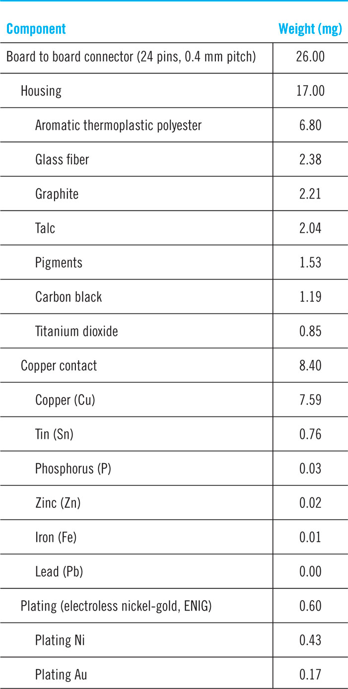
Table 6 shows the material declaration of a 24 pin board-to-board connector. This material composition is used by Proske et al. for the life cycle inventory model and scaled per pin number. The plating is assumed to consist of 71% nickel and 29% gold according to a material declaration of a similar connector.
Material declaration of board-to-board connectors.

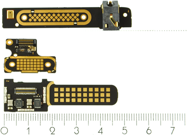
The mating counterparts on the module boards are Ni/Au pads on the printed circuit boards (Fig. 13).
Contact pads on Fairphone 2 receiver, rear camera, and display module boards.

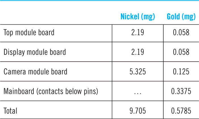
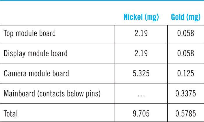
The amount of Ni and Au on the module boards is estimated based on the material composition of the PCB panels and allocated to the connector pads and other circuitries. The amount and Ni and Au for the pads is calculated, as listed in Table 7. More than 0.5 mg of gold is plated on the module PCBs just for the contact areas.
Ni and Au content for module PCB contact areas.
Additional printed circuit board area
The total PCB area in this smartphone model is 72.38 cm2.
The additional PCB to enable the board-to-board connectors adds up to the following:
(i) Mainboard (12 layers): 9.86 cm2
(ii) Display board (4 layers): 2.70 cm2
(iii) Top module board (4 layers): 2.88 cm2
(iv) Bottom module board (4 layers): 0.72 cm2
(v) Camera module board (4 layers): 1.47 cm2
In total, the PCB area required for connectors is 24% of the total board area and is as such a significant hardware overhead just to enable modularity.
Module housings
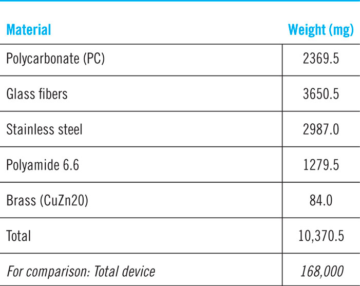
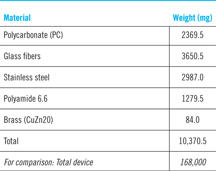
Housing of modules is required to protect the electronics and also for shielding purposes. For such sub-housing, the resulting materials are displayed in Table 8. The weight share of sub-housing materials is 6.1% of the total device weight.
Material for sub-housings.
LCA of modularity parts
Proske et al. assessed the Fairphone 2 in several impact categories, which represent a selection of major environmental aspects as defined in the scoping phase of the LCA:
(i) Global warming potential (GWP), 100-year time horizon, expressed in CO2-equivalents, and closely related to fossil fuel consumption, but in particular semiconductorReference Russ, Bipp, Jantschak, Stiewe, Cedzich and Dietrich34,Reference Boyd35 and display36–38 manufacturing emits non-energy-related greenhouse gases
(ii) Resource depletion includes abiotic resource depletion of elements, i.e., mineral resources, in antimony equivalents and of fossil fuels expressed in megajoules (MJ)
(iii) Human toxicity potential expressed in dichlorobenzene (DCB) equivalents
(iv) Terrestrial ecotoxicity potential in DCB equivalents, representing toxicity impacts on ecosystems, excluding aquatic systems
The “modularity parts” make up 2–13% of the production phase impacts depending on the impact category and are for most impact categories mainly connected to the additional PCB area. For the category abiotic resource depletion, the use of gold in connectors and on the PCB is dominating (see Table 9). The high impact of gold is partly compensated, if a high recycling rate is assumed as the recovery of precious metals is close to 100% in a copper or precious metal smelter. Take-back and collection is the major uncertainty in this equation.
LCA results: Fairphone 2 modularity (cradle to gate).
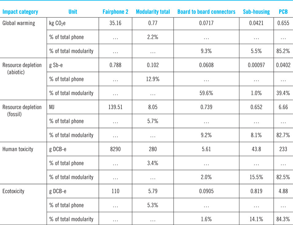
Modularity comes at the expense of moderately higher environmental impacts for device production (cradle-to-gate: from mining to final product assembly). This has to be outweighed by the intended lifetime extension through better reparability and upgradability. Proske et al.Reference Proske, Clemm and Richter33 analyzed a repair scenario with an assumed use time of five years (instead of 3 as an assumption for a standard smartphone use time, although some sources indicate that 2 years might be a more appropriate proxyReference Wieser39,Reference Tröger, Wieser and Hübner40 ) and an average number of repairs. This repair scenario has a positive effect seen across the whole life cycle and reduces the global warming potential by 30% per year of use. Positive effects are similar for most of the other assessed impact categories.
Recyclability
As a side effect, modularity also enhances recyclability, i.e., better separation in distinct mass flows for recycling.Reference van Schaik and Reuter16 As per European legislation, the battery of a smart mobile device has to be removed prior to recycling, the modular design simplifies this separation process and even leads as a side effect already to better separated fractions of other materials (battery to battery recycling, display to light metals recycling, cover to plastics recycling, and remaining parts to copper or precious metal smelter). Recyclability is important for the recovery of valuable resources, but as the LCA above indicates, lifetime extension is the primary environmentally motivated target of modularity.
Economic aspects of modularity
As the environmental analysis shows, there is an environmental and material overhead of modularity. From a sustainability perspective, modular design only pays off, if the devices do not come at prohibitive additional costs. A discussion of economic aspects complements the environmental analysis. The most evident cost saving for consumers is the anticipated need to purchase a new device less often, but other highly relevant cost effects of modular smartphone designs occur throughout the whole lifetime of a device.
Product costs
Product costs are all those costs born initially by the manufacturer, but with a likely effect on sales prices of the device:
Additional material costs: Although relevant in the LCA results above, additional material costs are in the cent range, given that the total raw material value is approximately 1 USD or € (own estimate based on material composition data and recent raw material prices).
Additional component costs: These are mainly costs for additional printed circuit board area, but also connectors. Spring-loaded contact pins are priced at several 10 cents per piece, easily adding up as a significant cost factor. Board-to-board mezzanine connectors are in a price order of magnitude of 10 cents each, if several 10,000 units are ordered.41
Product development: Total investments by Fairphone for the product development and engineering, design engineering of the Fairphone 2 are 14.67 €,42 of which a not distinguishable share is for designing in the modularity, but compared with the initial sales price of 525 € for the Fairphone 2, these modularity development costs are safe to say in the 1–2% range of total product costs.
Including material and component costs, the costs for modularity are estimated to be below 5% of the product costs.
A challenge for manufacturers of modular, thus intended, long-living smartphones is stocking of spare parts.43 As components in the ICT sector are subject to obsolescence, a last-time-buy might be needed to put spare parts on stock. The required amount of spare parts over time is highly speculative and ties up capital.
In a different kind of business model development, costs might even decrease significantly: The PuzzlePhone concept builds on an ecosystem of third parties developing smartphone modules. Developing only the main electronics part of the phone, but being relieved from the task to integrate the display, which comes as a separate module, is supposed to reduce development time and costs of a new phone significantly. This is likely to have a cost reduction effect for the user as well.
Repair costs
Repair costs in case of a DIY modularity are significantly lower as only parts costs and shipping of spare parts is charged, not the labor costs for repair, which can be significant. Typical prices to exchange an integrated battery of a smartphone are in the range of 20–50 € plus price of the replacement battery. Consequently with the first DIY repair already the additional price of the modular design is set off. This argument holds true only if the user is actually embracing the concept of DIY repairs, and if repairs involve only a very low risk to break other parts of the device.
Regarding the internal modularity and professional repairs, each repair case might come at a slightly lower price than for repairs of conventional designs, but for a professional repair shop, anyway the actual repair process is much less time consuming than pre- and post-repair testing. Labor time saving due to internal modularity is less relevant. The question is rather if a broken part can be replaced (at moderate parts costs) instead of having a case, where spare parts costs are excessive, e.g., replacing the whole monoblock mainboard with all its high-priced components is needed.
Disposal costs
Although modular designs enhance the recyclability of individual materials and parts, the economic value accessible through this separation is rather low (see raw material costs above). The process of taking the device apart is a bit faster for the preprocessor of the electronics waste. The saved labor costs are in the cents range.
Discussion
Modularity of smartphones can serve multiple purposes and can reflect various use and business scenarios. The variety of modularity concepts is huge. This research proposed a systematic classification of modularity types, which helps guide the discussion about intentions and sustainability effects of the various design approaches. Modular product designs increase the material consumption and the environmental footprint. The presented research is not the first indicating this conflict; this has been concluded already for a modular mobile digital device by Pamminger et al.Reference Pamminger, Glaser, Wimmer and Podhradsky44 and for a modular stationary ICT device by Vaija.Reference Vaija45
Upgrading in theory can help keep a device much longer. For a detailed analysis of this upgrading effect, further technical difficulties have to be addressed, such as hardware compatibility and, in particular, software support.
Modularity is an appropriate approach for a circular design, but the user is key for a materialization of the theoretical benefits: Only if the product in the end is really used longer through embracing the modularity features, the sustainability benefits will materialize. How to predict reliably user behavior (e.g., willingness to upgrade in a few years, willingness to perform simple repairs of high-tech products) for a disruptive product concept not yet introduced to the market (e.g., modular smartphones) is still an open question.
A design conflict also exists between product durability and modularity. Durable design can lead to significant lifetime extension effects, even as consumer repairs are not intended by design, see indications for long-term use of, e.g., iPhones.46
There is an evident link between modularity and some materials with sustainability issues. Modularity might reverse the trend toward reduced gold content in mobile ICT,Reference Schischke, Nissen and Lang10 increase the use of beryllium, although on a very low level, and of neodymium, for which recycling process still have to be put in place.
Acknowledgments
The research presented in this paper is an outcome of the project sustainablySMART. The project has received funding from the European Union’s Horizon 2020 research and innovation program under grant agreement no. 680640.