I. INTRODUCTION
Organic photovoltaic devices (OPVs) have attracted much attention because of their ease of fabrication, low cost of production, and mechanical flexibility.Reference Dennler and Sariciftci1,Reference Myers and Xue2 Since the first report on heterostructure OPVs with power conversion efficiencies (PCE) of ∼1% under an air-mass (AM) of 1.5 global illumination by Tang in 1987,Reference Tang3 several studies have demonstrated that the incorporation of traditional phthalocyanine (Pc) materials can significantly enhance the device performance.Reference Peumans and Forrest4 In general, Pc materials such as copper phthalocyanine (CuPc),Reference Peumans and Forrest4 zinc phthalocyanine (ZnPc),Reference Gebeyehu, Maennig, Drechsel, Leo and Pfeiffer5 subphthalocyanine (SubPc),Reference Gommans, Cheyns, Aernouts, Girotto, Poortmans and Heremans6 and tin(II) phthalocyanine (SnPc),Reference Inoue, Yamagishi and Yamashita7 and fullerene C60 have been used as typical electron donors and electron acceptor materials in OPV systems due to their high absorption coefficients and suitable energy levels. Considering the tandem device toward high efficiency, the absorption from both long and short wave lengths should be taken to extend the spectral coverage, for which conventional Pc materials only absorb the long wave length range. From this point of view, the other molecular materials for OPVs based on the donor–acceptor (D–A) structure, examples of which include triphenylamine derivative,Reference Alévêque, Leriche, Cocherel, Frère, Cravino and Roncali8 4,4′,4″-tris[3-methylphenyl(phenyl)amino] triphenylamine (m-MTDATA),Reference Hong, Lee, Lee, Li and Shirota9 N,N′-diphenyl-N,N′-bis(3-methylphenyl)benzidine (TPD),Reference Osasa, Yamamoto and Matsumura10 N,N′-diphenyl-N,N′-di(α-naphthyl)-benzidine (α-NPD)Reference Kushto, Kim and Kafafi11 and others,Reference He, He, Yi, Wu, Bai, Shuai and Li12 should be introduced. However, such typical D–A structure based materials exhibit PCEs of 0.1–1.3% under AM 1.5 illumination, much lower than the Pc-based OPVs.Reference Heremans, Cheyns and Rand13,Reference Rand, Cheyns, Vasseur, Giebink, Mothy, Yi, Coropceanu, Beljonne, Cornil, Brédas and Genoe14
Recently, some efficient OPVs based on novel functional materials have been demonstrated. In 2006, a p-n heterojunction device using a D–A structure of dicyanovinyl-substituted tris[4-(2-thienyl)phenyl]amine and C60 was reported to obtain a PCE ∼1.8%.Reference Cravino, Leriche, Alévêque, Roquet and Roncali15 More recently, Shirota et al.Reference Kageyama, Ohishi, Tanaka, Ohmori and Shirota16 reported on a different possible approach to high performance OPVs, consisting of the incorporation of amorphous donor material, tris[4-(5-phenylthiophen-2-yl)phenyl]amine (TPTPA), due to its fast carrier mobility. Their group reported that an OPV using TPTPA exhibited a PCE of 1.7% with fullerene C60 as the electron acceptor and 2.2% with fullerene C70 as the electron acceptor. Meanwhile, some long wave length absorption electron donors, such as dicyanovinyl-appended oligothiophenes,Reference Uhrich, Schueppel, Petrich, Pfeiffer, Leo, Brier, Kilickiran and Baeuerle17 tetraphenyldibenzoperiflanthene,Reference Fujishima, Kanno, Kinoshita, Maruyama, Tanaka, Shirakawa and Shibata18 and diindenoperylene,Reference Wagner, Gruber, Hinderhofer, Wilke, Bröker, Frisch, Amsalem, Vollmer, Opitz, Koch, Schreiber and Brütting19 have been proposed to achieve high performance. More recently, some D–A structure based materials have been reported to be showing a PCE of more than 3% in vacuum-deposited planar bilayer OPVs.Reference Kronenberg, Steinmann, Bürckstümmer, Hwang, Hertel, Würthner and Meerholz20–Reference Steinmann, Kronenberg, Lenze, Graf, Hertel, Meerholz, Bürckstümmer, Tulyakova and Würthner22 Hence it is desirable to explore more stable materials, as they may greatly improve the performance of OPV devices.
In a previous report, Chen et al.Reference Lee, Chiang and Chen23 demonstrated bright red organic light-emitting diodes (OLEDs) using a 2,3-Bis(2-(diphenylamino)-9,9′-spirobifluorene-7-yl)fumaronitrile (PhSPFN) as the emitting host. They also reported that PhSPFN is a high-performance material for nondopant white OLEDs because of its appropriately suitable highest occupied molecular orbital (HOMO: 5.6 eV) and lowest unoccupied molecular orbital (LUMO: 3.6 eV) levels. With properties like these, we expect that PhSPFN is perfectly suitable as an electron donor in OPVs for achieving a high open-circuit voltage (V OC) and performance due to the large energy gap between the HOMO of the PhSPFN donor and the LUMO of the C60 acceptor.Reference Opitz, Wagner, Brütting, Salzmann, Koch, Manara, Pflaum, Hinderhofer and Schreiber24 Herein, we worked at developing high-performance OPVs using the short wave length absorption material PhSPFN as the electron donor to obtain an efficient device. In our PhSPFN OPV, the device shows high performance with a V OC of 0.91 V, short current density (J SC) of 3.9 mA/cm2, fill factor (FF) of 56%, and PCE of 2% under air-mass (AM) 1.5 global (G) illumination at a light intensity of 100 mW/cm2. For studying the impact of the interface band gap (I g) on the V OC, a series of donor materials such as m-MTDATA, NPB, PhSPFN, and ADN with different HOMO levels were used in the OPVs for comparison.
II. EXPERIMENTAL
The devices were fabricated on precleaned indium tin oxide (ITO) glass with a sheet resistance of 10 Ω/sq. After solvent cleaning, the substrates were treated with high power O2 plasma to achieve a work function of 5.60 eV.Reference Liu, Su, Lee, Lin, Yeh, Chen and Lee25 C60 and bathocuproine (BCP) were purchased from Uni-Onward Corp. (Taiwan), PhSPFN was synthesized in the laboratory according to a standard procedure.Reference Lee, Chiang and Chen23 All materials mentioned above were purified by gradient sublimation in a home-built tube before loading into the thermal chamber for use. The evaporation rates of the organic and metal layers were regulated at 0.1 nm/s by an individual quartz-crystal monitor and were calibrated by a series of thickness measurements of each layer with a surface profiler (Veeco Dektak 150). Subsequently, the current density–voltage (J–V) characteristics of the OPVs were measured in the dark and under an air mass (AM) of 1.5G solar illumination from a class A solar simulator (Newport 91160A, Irvine, CA) with a programmable source meter (Keithley 2400, Cleveland, OH). The light intensity was calibrated using a Si photodiode (PVM 172; area = 3.981 cm2) from the National Renewable Energy Laboratory. Electrical characteristics of the PhSPFN OPVs, ITO/PhSPFN (x nm)/C60 (40 nm)/BCP (10 nm)/Al, incorporating six different donor thicknesses [x = 3, 5, 7, 9, 11, and 13 nm, and the corresponding PhSPFN OPV designated as PhSPFN1, PhSPFN2, PhSPFN3, PhSPFN4, PhSPFN5, and PhSPFN6, respectively] were analyzed. For the determination of external quantum efficiency (EQE), a monochromator (Newport 74100, Irvine, CA) was used to select the wave length impinging on the device under testing. The photocurrent was measured using a lock-in amplifier (Signal Recovery 7265, Oak Ridge, TN) that was referenced to a chopper with a frequency of 250 Hz. The work function or HOMO levels of the ITO or donor materials were measured by a photoelectron spectrometer (Riken Keiki AC-2, Union City, CA). This measurement uses an open counter, which is a unique counter that can detect and count photoelectrons in the air. The monochromatized ultraviolet photons were used to excite the photoelectron from the sample under test. Once the photon energy becomes higher than the work function or HOMO level of the sample, the photoelectron is emitted and detected by the open counter. As a consequence, the on-set point of the photoelectron spectroscopy corresponds to the work function or the HOMO level of the samples. More experimental details can be found in the literature.Reference Kirihata and Uda26,Reference Noguchi, Nagashima and Uda27 Note that the work function of ITO was identical to the results obtained from ultraviolet photoelectron spectroscopy (UPS) (see Supporting Information for experimental details and discussion). The capacitance–voltage (C–V) characteristics of the OPV devices were determined using a frequency response analyzer (Solartron 1260, Oak Ridge, TN) with a frequency of 1000 Hz and an ac signal of 50 mV. All measurements herein were carried out in an air environment.
III. RESULTS AND DISCUSSION
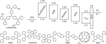
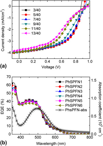
To obtain high OPV performance, the energy levels and carrier mobility of the electron donor are very important issues for OPVs in terms of the PCE.Reference Lin, Liu, Lee, Hunag, Su, Chiu, Chen and Lee28–Reference Guerrero, Marchesi, Boix, Ruiz-Raga, Ripolles-Sanchis, Garcia-Belmonte and Bisquert30Figure 1 shows the chemical structures of PhSPFN, C60, and BCP. We determined the HOMO and LUMO energy levels of PhSPFN with a photoelectron spectrometer to be 5.60 and 3.45 eV, respectively.Reference Lee, Chiang and Chen23 It is well known that a wide I g between the HOMO level of the donor and LUMO level of the acceptor will result in a high V OC.Reference Lin, Liu, Lee, Hunag, Su, Chiu, Chen and Lee28,Reference Rand, Burk and Forrest31,Reference Mutolo, Mayo, Rand, Forrest and Thompson32 Accordingly, PhSPFN exhibits a high I g ∼ 1.4 eV, where a high value of I g becomes a major factor in achieving a device with a high V OC.Reference Lin, Liu, Lee, Hunag, Su, Chiu, Chen and Lee28,Reference Guerrero, Marchesi, Boix, Ruiz-Raga, Ripolles-Sanchis, Garcia-Belmonte and Bisquert30,Reference Perez, Borek, Forrest and Thompson33 As a step in the optimization of the PhSPFN cell, we studied the dependence of OPV performance as a function of donor thickness. Figure 2(a) shows measurement data for J SC, V OC, FF, PCE, shunt resistance (R SH), and series resistance (R S), as summarized in Table I. As is evident from Table I, the performances of PhSPFN1 and PhSPFN2 devices are higher than those of the other PhSPFN cells. The FF increases monotonically with decreasing PhSPFN thickness, while the J SC remains unchanged, except for PhSPFN6 with a value of ∼3.77 mA/cm2. Hence these data suggest that the optimal efficient OPV performance should be obtained with an ultrathin PhSPFN layer from 3 to 5 nm. This is presumably due to the greater charge balance of PhSPFN/C60 in the OPV system, resulting in an increased carrier collection efficiency.Reference Li, Shrotriya, Huang, Yao, Moriarty, Emery and Yang34,Reference Mihailetchi, Xie, de Boer, Koster and Blom35
Chemical structure and device configuration for the donor/C60 OPV devices with various donor materials, m-MTDATA, NPB, PhSPFN, and ADN.

(a) Photocurrent characteristics and (b) EQE of a planar heterostructure of PhSPFN/C60/BCP/Al OPVs with six different thicknesses of PhSPFN/C60 nm: 3/40 (square symbol), 5/40 (circle symbol), 7/40 (triangle symbol), 9/40 (inverse triangle symbol), 11/40 (diamond symbol), and 13/40 (left triangle symbol).

Electrical characteristics (J SC, V OC, FF, R SH, R S, and PCE) of OPVs: ITO/PhSPFN (x nm)/C60 (40 nm)/BCP (10 nm)/Al (100 nm).

On the other hand, an S-shaped response in J–V is clearly observed when the thickness of PhSPFN is increased from 9 to 13 nm. We believe this is attributable to the fact that the imbalanced carrier mobilities between the donor and acceptor results in charge accumulation, which further causes carrier recombination.Reference Wang, Ren, Shi, Leung and Chan36 In cases where PhSPFN thicknesses are greater than 7 nm, the electric field distribution is most probably moved to the anode side because the hole mobility of PhSPFN may be too low as compared with the electron mobility of C60 (0.3–0.5 cm2/V s).Reference Tress, Petrich, Hummert, Hein, Leo and Riede37–Reference Aernouts, Geens, Poortmans, Heremans, Borghs and Mertens39 Thus, the series (shunt) resistance increases (decreases) with increasing PhSPFN thickness in our OPVs, whereas the optimal film thickness of D–A is necessary to collect more hole and electron carriers.Reference Peumans, Yakimov and Forrest40–Reference Sievers, Shrotriya and Yang42 In addition, we have observed that such a high V OC depends not only on a high I g value but also on the thickness of PhSPFN, which exhibits an increased V OC as the thickness of PhSPFN is increased (see Table I). Accordingly, V OC is defined as the voltage at which the injection current equals the photocurrent, i.e., the open-circuit condition, or the voltage at which charge generation is equal to charge recombination.Reference Nelson, Kirkpatrick and Ravirajan43 As the device is operated close to the short-circuit condition, the photocurrent is dominated by a diffusion mechanism rather than drift transport due to the absence of large amounts of injection current.Reference Lin, Zhang, Liu, Chiu and Lee44 When we operate the OPV with an applied voltage near the V OC, competition between the injection and diffusion currents occurred. In this case, the distribution profile of the electric field into the OPV may decrease, and the injection current will correspondingly be reduced as the thickness is increased. This indicates that a higher voltage is required to compensate for the photocurrent with the injection current in thicker PhSPFN devices. Therefore, PCE reaches a minimum value of 1.4% and V OC exhibits a peak voltage of 0.97 V with a 13-nm thick PhSPFN. Note that similar findings have been made in other studies.Reference Giebink, Wiederrecht, Wasielewski and Forrest45,Reference Ravirajan, Haque, Durrant, Poplavskyy, Bradley and Nelson46 Although the carrier mobility of PhSPFN is rather low compared with the more recently identified D–A structure materials, the use of a thin layer in an OPV device may reveal possible applications in tandem cells, due to the short wave length absorbing property and the transparency of the thin donor, which allows more light to pass through to the subcells with complementary absorption.
The spectral dependence of the EQE of PhSPFN cells measured under low light intensity is plotted in Fig. 2(b). It shows that the EQE efficiency over 350–500 nm decreases slightly with an increasing donor thickness of OPVs, while it increases slightly from 500 to 600 nm. This leads to the invariant J SC throughout our devices, except for the device with the greatest thickness (PhSPFN6). The changeless J SC could be interpreted as follows. As previously discussed, the collection efficiency in a thinner PhSPFN device is better than in a thicker one. However, the thinnest PhSPFN layer might place the D–A interface close to the ITO electrode, which is prone to quench excitons and results in a loss of photocurrent.Reference Hill, Zhu and Pan47 On the other hand, according to the periodicity of light interference, excitons generated at longer wave lengths are much closer to the ITO anode.Reference Pettersson, Roman and Inganas48,Reference Monestier, Simon, Torchio, Escoubas, Ratier, Hojeij, Lucas, Moliton, Cathelinaud, Defranoux and Flory49 Therefore, in thicker PhSPFN, the photocurrent could originate from the longer wave lengths at around 500–600 nm (as predicted by the simulation but not shown here), despite the reduced carrier transport property. In some manner, not fully understood at this point, the charge collection efficiency compensates for the loss of photocurrent and therefore retains the same J SC for PhSPFN devices with thicknesses ranging from 3 to 11 nm. In the case of the thickest device, with 13-nm thick PhSPFN, the charge collection is poor, which may be due to the low hole mobility of PhSPFN and hence the low J SC as compared with the other devices. In addition, the absorbance loss in C60 as observed in the EQE near 350 nm may also impact upon the reduced J SC.
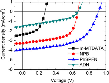
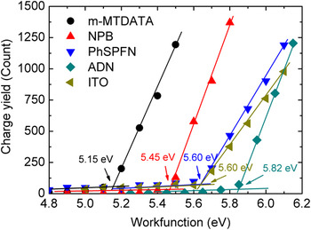
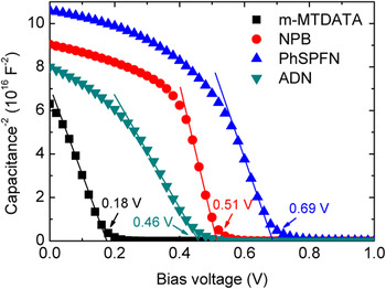
A variety of donors were used in our optimum structure, ITO/donor (5 nm)/C60 (40 nm)/BCP (10 nm)/Al, to study the dependence of the HOMO level and ITO/donor interface on the V OC. Figure 1 shows the chemical structures and electronic configurations of m-MTDATA,Reference Shirota, Kuwabara, Inada, Wakimoto, Nakada, Yonemoto, Kawami and Imai50 NPB,Reference Barth, Muller, Riel, Seidler, Riess, Vestweber and Bassler51 PhSPFN,Reference Lee, Chiang and Chen23 and ADN.Reference Culligan, Chen, Wallace, Klubek, Tang and Chen52 The electrical properties of various devices are shown in Fig. 3. Regardless of the transport properties, no S-shaped curve is observed for any device, indicating a charge imbalance condition in the OPV and that light absorption by the donor layer could be neglected when the donor thickness is less than 5 nm.Reference Zhang, Wang and Tang53 The photovoltaic parameters are summarized in Table II. Interestingly, the highest performance (V OC, J SC, and PCE) was obtained from the ITO/donor or D/A interface of the ITO/PhSPFN/C60 structure. To understand this phenomenon, the HOMO levels of all donor materials were characterized and are shown in Fig. 4. As compared with PhSPFN (5.60 eV), the device using an m-MTDATA (5.15 eV) or NPB (5.45 eV) donor shows a reasonably low V OC due to the small I g when in contact with C60. Those HOMO levels are not energetically aligned to ITO (5.60 eV), resulting in a loss in hole extraction efficiency at the interface with the ITO/donor and reduced J SC in the OPV (see Table II). Note that this issue is very similar to inserting a buffer layer between the ITO and donor to increase the hole extraction efficiency and built-in voltage in the device.Reference Kulshreshtha, Choi, Kim, Jeon, Suh, Park and Kwon54 On the other hand, the variant J SC may also arise from the different absorption profiles and D/A properties using different donor materials. The former reason is ruled out due to the unchanged optical field distribution for all OPV devices with different donor materials (not shown here). Therefore the latter reason, including energy level offsets of the HOMO and LUMO, electronic structures, and the carrier transport between donor and acceptor materials may be the explanation.Reference Rand, Burk and Forrest31,Reference Servaites, Ratner and Marks55 However, this is beyond the scope of this article. In contrast to the improved V OC when increasing I g, no increase in V OC was obtained when we used extremely low-lying HOMO materials, i.e., ADN (5.82 eV), in which no barrier is present for hole extraction. This may indicate that a higher HOMO level of the donor with respect to the work function of the anode may not be suitable, but an energetically matched contact is critical for efficient hole extraction and a high V OC. On the other hand, the LUMO-LUMO offset between donor and acceptor may also influence the V OC due to different carrier separation efficiency.Reference Rand, Burk and Forrest31 However, it is difficult to understand this effect without a well-constructed simulation model. To further confirm the origin of the variant V OC, the C–V characteristics of the OPV devices were measured, as shown in Fig. 5. Note that the nonlinear curves at the lower bias voltage are due to the limitations in geometry of the capacitance, and they tend to saturate at similar values. The intersection of the extrapolating line and the voltage axis determines the built-in potential (V bi), which shows good agreement with the measured V OC. It is ascertainable that too high a HOMO level may not be appropriate for optimizing V OC unless the anode contact has been suitably modified.
J–V characteristics of devices using various donors (m-MTDATA, NPB, PhSPFN, and ADN) with a thickness of 5 nm.

Electrical characteristics (J SC, V OC, FF, R SH, R S, and PCE) of OPVs: ITO/donor (5 nm)/C60 (40 nm)/BCP (10 nm)/Al (100 nm).

Low-energy photoelectron spectroscopy of thin films from various donors (m-MTDATA, NPB, PhSPFN, and ADN).

C–V characteristics of thin-donor OPV devices with various donor materials. The extrapolating lines from the on-set points indicate the V bi.

IV. CONCLUSION
In summary, an efficient OPV using novel PhSPFN as the electron donor has been fabricated. The performance of the PhSPFN-based OPV is better than other ultrathin donor OPVs, although the absorption spectrum of PhSPFN is not extensive. Due to the PhSPFN having a high I g value of ∼1.4 eV, the V OC of PhSPFN OPV is greater than those based on amorphous materials. Moreover, the energy alignment between the HOMO of the donor and the work function of the anode is demonstrated to play an important role in the optimization of V OC and J SC. Although ADN has the highest I g, a significantly reduced V OC was observed, most probably due to the unmatched work function of the ITO to HOMO level. The built-in potential estimated from C–V characteristic further confirms the importance of energy alignment between the anode and HOMO of the donor in improving the V OC.
ACKNOWLEDGMENTS
The authors acknowledge the Academia Sinica of Taiwan and financial support from the National Science Council (Grant Nos. NSC 100-3113-E-001-001, NSC 100-2218-E-131-001, and NSC 101-2221-E-131-025). Special thanks go to Mr. Ted Kao, Uchi Optoelectronic (Malaysia) Sdn. Bhd., for the donation of research equipment (Flexible Optoelectronic Device and Processing Laboratory, MCUT).