I. INTRODUCTION
Ultra-wideband (UWB) technology has received huge attention in the wireless world to satisfy the ever increasing demand for large data rate. The frequency band of 3.1–10.6 GHz is allocated to the UWB application by the Federal Communications Commission (FCC) in 2002. The bandwidth requirement for UWB system is described by two ways, either 10 dB return loss bandwidth is larger than 25% of center frequency or bandwidth equal to or >1.25 GHz if center frequency is >6 GHz within range of 3.1–10.6 GHz [1].
Owing to extremely large bandwidth, UWB system cause interference to other pre-allocated narrow band communication systems such as wireless local area network (WLAN) with center frequencies of 2.4 GHz (2.4–2.484 GHz), 5.2 GHz (5.15–5.35 GHz), and 5.8 GHz (5.725–5.825 GHz), World interoperability for microwave access (WiMAX) with center frequencies of 2.5 GHz (2.5–2.69 GHz), 3.5 GHz (3.4–3.69 GHz), and 5.8 GHz (5.25–5.825 GHz), Satellite digital multimedia broadcasting (S-DMB) with frequency band 2.63–2.655 GHz [Reference Dong2]. To reduce electromagnetic (EM) interference with these pre-exciting systems, two possible solutions are either design a source pulse that has zero power spectral density (PSD) at above-mentioned bands or to design an ultra-wideband antenna with band-notched characteristics that stops radiating at above-discussed bands. Various band-notched techniques are reported in [Reference Su, Wong and Chang3–Reference Bahadori and Samii8], such as half-wave length slots on radiator or ground, λ/4 length open ended slot on patch (V-, arc-, U-, H-, and F-shapes) and use of parasitic elements. Parasitic loading techniques to create notch at transmission band requires multiple resonator when multiple band-notches are required, which is a major drawback. Moreover, large conductor size and mutual coupling between the resonators adds to the worst.
To overcome these limitations dual-band-notched antenna is proposed using CPW feed resonator and a slot realized on the radiator. Operation of CPW resonator is independent of size or shape of radiating patch. During designing of CPW resonator, notch frequency is precisely modified/tuned just by changing the physical dimension of the resonator. CPW feeding is used because of good performance at higher frequency, simple, and cost-effective manufacture due to single-side metallization.
In this paper, antenna design and simulations have been carried out using CST microwave studio V12 with MATLAB 2010a for time-domain analysis and received pulse generation. The proposed antenna has been fabricated using LPKF ProtoMat S100. Performance parameters, e.g. return loss measurement has been carried out using Agilent PNA series vector network analyzer, far-field radiation pattern at different frequencies of both E- and H-planes, and gain measurements have been carried out in an anechoic chamber. The time-domain characteristics of the proposed antenna were carried out in an open environment with random scattering objects using two identical prototype antennas.
II. ANTENNA DESIGN AND RETURN LOSS
Figure 1(a) shows the geometry of the proposed UWB monopole antenna with dual-band notch. The antenna has been simulated on an FR-4 substrate with dielectric constant 4.4 and thickness of 1.524 mm. The characteristic impedance of CPW feed line can be set by just changing width of center feed line and gap between feed line and ground. The width of the microstrip feed line that is soldered to the Sub-Miniature version A (SMA) connector and the gap between the feed line and ground has been chosen to achieve the characteristic line impedance of 50 Ω at the connecting port. A bandwidth enhancement technique using rectangular bevel cut has been analyzed with the help of full-wave EM simulator. Layout of CPW-fed antenna without any stepped cut and antenna with cut at the upper corner of the patch with their simulated return loss has been shown in Fig. 1(b). The systematic design procedure that leads to the final prototype of the antenna has been shown in Fig. 1(b). The antenna labeled “A” shown in Fig. 1(b) is the initial CPW-fed antenna, which is matched in the lower band of the desired bandwidth (3.1–10.6 GHz). Beveling the lower corner of the patch with a single rectangular shape cut (labeled “B”) improves the matching at higher band and increases the impedance bandwidth as shown in Fig. 1(b). By introducing rectangular cuts at lower corner of the patch and upper corner of the ground, the impedance bandwidth increases. The dimensions of the cuts has been parametrically optimized, so that the fundamental mode coupled with higher-order mode resonances are occurred due to stepped lengths of patch and ground, which improves matching over the wide-band frequency spectrum. The level of impedance matching of both antennas, i.e. without notch and with notch function, throughout the bandwidth is similar except at the dual notch bands. The final optimized antenna with dual-band notch has been shown in Fig. 1(a) and the simulated return loss in Fig. 1(b) labeled as “C”.
(a) Schematic representation of the proposed dual notch antenna; (b) simulated return loss. (FD = 3.0, G1 = 0.4, Y = 1.1, P = 7.4, L1 = L3 = L5 = 3.0, L2 = L4 = 2.0, L6 = 3.0, P1 = 10.5, P2 = 6.0, G2 = 2.0)(unit: mm).

In the proposed antenna, a slot at the upper portion of the antenna has been created, which creates a notch at lower 3.5 GHz band and the simultaneous CPW resonator has been used to get the second band notch at 5–6 GHz band. CPW resonator has advantages like resonance frequency is easily changed by changing the length of the resonator, the bandwidth of rejected band is varied by changing the position of resonator. The antenna geometry is unaffected by changing the center frequency of rejected band at 3.5 GHz and/or at 5–6 GHz band by changing the dimensions of upper slot and/or CPW resonator incorporated to center conductor of CPW-feed section.
Both the notch bands can be tuned by changing the physical dimensions of the slots. Figure 2 shows the effect of parametric variations of the slots parameters on return loss performance. The notch frequency varies inversely with the slot dimension, which is in accordance with the frequency wavelength relations. Increasing slot lengths increase the current patch, hence the notch frequency moves to the lower side (Fig. 2(b)). The mutual coupling between slot and CPW resonator is very less. So, these resonators are good candidates to achieve multi-band notched characteristics in UWB antenna. Figure 2(a) shows the parametric analysis of CPW resonator length “P” on return loss performance. Increasing the length moves the notch peak towards left, i.e. the lower band of matched bandwidth. The bandwidth of the notch band remains unaffected to the change in length of CPW resonator. Tunning of the notch band have a little effect on the impedance bandwidth except at notch band.
Parametric variations of the proposed antenna.
Surface current distribution on the antenna has been shown in Fig. 3. To have a deeper insight on the resonant behavior of antenna, surface current distribution has been analyzed at discrete frequencies of 3.5, 5.8, and 10 GHz. At 3.5 GHz maxima of surface current is concentrated around the upper slot and at 5.8 GHz around the CPW resonator, giving rise to the band-notched characteristic. Unlike narrow-band antenna, the UWB antenna behaves in a traveling wave type that supports both fundamental mode of propagation at lower frequency and higher-order modes at higher frequencies. Surface current at 10 GHz shows a complex pattern due to the higher-order mode generation. Effective coupling between different resonance modes gives wide-band matched impedance bandwidth.
Surface current on the antenna at: (a) 3.5 GHz, (b) 5.8 GHz, and (c) 10 GHz.
III. FABRICATION AND MEASURED RESULTS
To measure the time-domain performance of the proposed dual-band-notched antenna, two identical antennas with equal dimensions has been fabricated and measured. Figure 4 shows fabricated antennas and the measured return loss for both antennas. The measured return loss of both the fabricated antennas is quite similar and in accordance to the simulated return loss except at (11–12 GHz) band w.r.t. level of matching (Fig. 4(a)). Both fabricated antennas successfully operate with an extended impedance bandwidth (measured at 10 dB return loss) covering the FCC recommended 3.1–10.6 GHz band. Dual-band notch was achieved exactly at 3.5 and 5–6 GHz, but the measured notch strength little less than the simulated. Measured results are in accordance with the simulated results with acceptable tolerance level. Generally, it is desired that the far-field radiation pattern of an UWB antenna should be omni-directional and stable over the large impedance bandwidth. The omni-directional nature of the pattern limits the realized gain compared to a directional antenna. Again at higher frequencies, there is a higher realized gain compared to the lower frequency as the antenna becomes electrically large at higher frequencies. The measured gain of the fabricated antenna has been shown in Fig. 4(b). Since both the fabricated antennas are identical, gain plot of single antenna has been shown. The gain has been measured at discrete frequencies along the direction of maximum power reception using standard gain horn antenna DRH10 (amitec) with substitution/transfer method. Measured gain has a flat nature over the frequencies except at the notch bands. The dip in the gain is very narrow at the notch frequency, which can be observed from Fig. 4. The measured gain is <5 dBi over the entire bandwidth.
Measured (a) return-loss of both antennas, (b) gain of the antenna and the fabricated antennas.
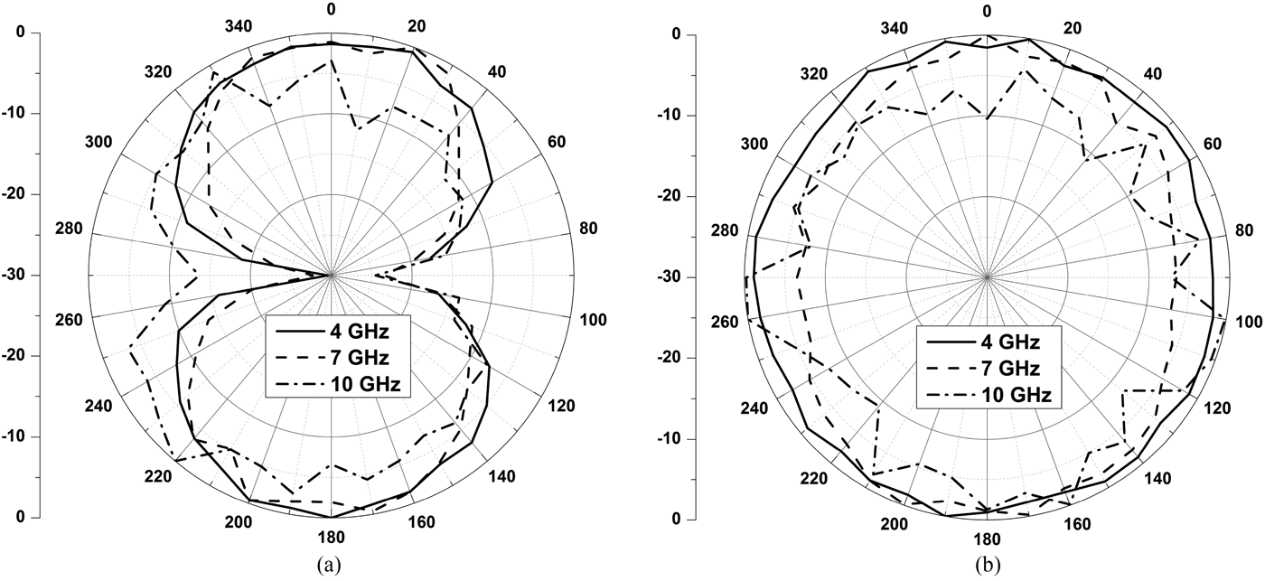
The measured normalized radiation patterns of the band-notched UWB antenna inside an anechoic chamber at different frequencies in both E- and H-planes have been shown in Fig. 5. The measured power patterns in H-plane are fairly omnidirectional over the entire band. It shows the doughnut-shaped pattern at lower 4 GHz, which is similar to a conventional monopole in free space. The E-plane power patterns are dumbbell-shaped at the lower frequency and changes at higher band due to higher-order mode propagation.
Measured radiation pattern of the dual-band-notched UWB antenna at different frequencies in (a) E-plane, (b) H-plane.
IV. SYSTEM TRANSFER FUNCTION AND GROUP DELAY
The antenna system measurement has been carried out outside anechoic chamber considering the real-world situation with multiple reflecting objects. The antenna system involves two identical band-notched UWB antennas, transmitting and receiving are separated by a distance of 50 cm. The investigation of the system performance has been carried out in two different orientations. The antennas have been oriented face-to-face with each other for one measurement and side-by-side with each other for another measurement. The group delay variation of UWB antenna system is <1 ns in the entire band for both the orientations. In the S 21-parameter of band-notched UWB antenna system, there is a sharp dip at notch frequency for both the orientations. There is a sharp change in the group delay at the notch frequency in both the orientations for band-notched UWB antenna system because of the presence of phase nonlinearities (Fig. 6).
Measured system transfer function and group delay for band-notched UWB antenna system: (a) face-to-face, (b) side-by-side orientations (black line, S 21; red line, group delay).
V. SYSTEM FIDELITY FACTOR (SFF) AND RINGING DURATION
The antennas are assumed to be excited by the fourth derivative of the Gaussian pulse UWB signal, which satisfies the FCC power spectral mask for indoor communication [Reference Ma and Jeng9].
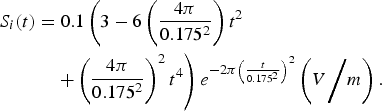 $$\eqalign{{S_i}\lpar t\rpar &= 0.1 \left(3 - 6\left( \displaystyle{4\pi \over 0.175^2} \right){t^2} \right. \cr & \quad \left. + \left( \displaystyle{4\pi \over 0.175^2} \right)^2 t^4 \right) e^{- 2\pi \left({t \over 0.175^2} \right)^2} \left(V \bigg{/} m \right).}$$
The frequency response of the system (S 21) is transformed to time-domain using Hermitian processing. As the first step, the pass-band signal is obtained with zero padding from the lowest frequency down to DC (zero frequency). After that, the conjugate of the signal is taken and reflected to the negative frequencies. The resultant double-sided spectrum corresponds to a real signal, which is the system impulse response. Inverse fast Fourier transform (IFFT) is used to obtain the impulse response in the time domain. Then the impulse response is convolved with the input signal to obtain the received signal.
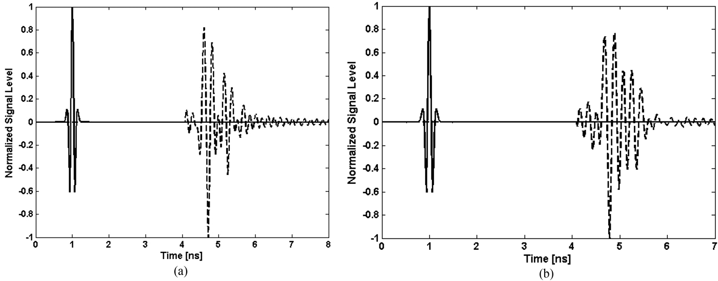
The SFF is defined as the cross-correlation between the normalized input signal T s (t) and normalized received signal R s(t) [Reference Ali-Akbari, Azarmanesh and Soltani10]. The SFF reaches unity as the two pulses are exactly the same in shape, which means that the antenna system does not distort the incident pulse at all. Figure 7 shows the normalized input signal and normalized received signal for both the orientations for band-notched UWB antenna system. The SFF for band-notched UWB antenna system in face-to-face and side-by-side orientations are 0.821 and 0.807, respectively.
 $$SFF = \mathop {\max }\limits_\tau \left({\left\vert {\displaystyle{{\vint_{ - \infty }^\infty {{T_s}\lpar t\rpar {R_s}\lpar t + \tau \rpar } \, dt} \over {{{\left[{\vint_{ - \infty }^\infty {\vert {T_s}\lpar t\rpar {\vert ^2}dt} } \right]}^{1/2}}{{\left[{\vint_{ - \infty }^\infty {\vert {R_s}\lpar t\rpar {\vert ^2}dt} } \right]}^{1/2}}}}} \right\vert } \right).$$
Ringing duration is calculated as the time required for the signal to attenuate from the maximum value of the signal to 5% of the maximum value of the signal. The ringing durations of the received signal for band-notched UWB antenna system in face-to-face and side-by-side orientations are significantly small. The transmitted pulse undergoes very minimum distortion. Hence, the received signal fairly retains the input pulse shape. This shows that the received signal is less susceptible to inter symbol interference (ISI).
Normalized received signals for band-notched UWB antenna system in (a) face-to-face orientation. (b) side-by-side orientation (solid line, input signal; dash line, received signal).
VI. CONCLUSIONS
In the present work, a compact UWB antenna with dual-band-notch characteristics at 3.5 and 5–6 GHz has been proposed. Using the CPW-feeding system good impedance match is achieved over the FCC-recommended band (3.1–10.6) GHz. Measured results show the H-plane radiation patterns are fairly omnidirectional and gain is <5 dBi over the entire UWB band. The system transfer function, group delay, ringing duration, and the SFF of band-notched UWB antenna system in face-to-face as well as side-by-side orientations are presented. The measured values indicate that the proposed dual-band-notched UWB antenna show acceptable pulse distortion. Hence, the proposed antenna well-satisfies the requirements for successful implementation in UWB applications. Compact size with notch band tune-ability by changing physical dimensions, consistent omnidirectional radiation patterns with ease of fabrication due to simplified single-layer structure without via and parasitic elements make antenna suitable for practical application.
Jagannath Malik is currently pursuing his Doctoral degree from Indian Institute of Technology Roorkee (IIT-R) in Electronics and Computer Department. He received his Integrated Dual Degree (Bachelors & Masters) in Electronics & Wireless Communication from Indian Institute of Technology Roorkee, India. His area of research includes Antenna, Soft computing techniques, and Millimeter wave designs. He has authored a number of research articles on Artificial Neural networks, Antennas, and one Book chapter on soft computing.
Parth C. Kalaria is currently pursuing his Doctoral degree from Institute for Pulsed Power and Microwave Technology (IHM), Karlsruhe Institute of Technology, Germany. He received his Master of Technology (M.Tech.) degree from Indian Institute of Technology Roorkee, India in RF & Microwave Engineering. His areas of expertise include Antennas, UWB techniques, and Millimeter wave source design. He is currently working toward High-power Gyrotron design for Fusion Reactors.
M.V. Kartikeyan was born in Nellore (Andhra Pradesh), India, in 1961. He received the M.Sc. and Ph.D. degrees in 1985 and 1992 in Physics and Electronics Engineering, respectively from the Banaras Hindu University, India. Dr., Kartikeyan is the recipient of a Hildegard-Maier Research Fellowship for Electrical Sciences of the Alexander von Humboldt Foundation and the Alexander von Humboldt Research Fellowship for long-term Cooperation and worked at the Institut für Hochleistungsimpuls- und Mikrowellentechnik, Karlsruhe Institute of Technology, Karlsruhe, Germany. He joined the Department of Electronics and Computer Engineering, Indian Institute of Technology, Roorkee, India, in 2003 as an Associate Professor and at present he is working as a Full-Professor. His research interests include Millimeter Wave Engineering (Electron Cyclotron Masers and otherHigh Power Devices and Components), Microstrip Antennas for Communications, Computational Electromagnetics, Microwave Integrated Circuits, and RF & Microwave Design with SoftComputing Techniques. Dr. Kartikeyan is a Fellow of the Institution of Electronics and Telecommunications Engineers (IETE), Fellow of the Institution of Engineers (IE), India, and Senior Member of IEEE.