Introduction
Recent years have seen significant progress in the two interrelated fields of plasmonics (or metal optics)Reference Ritchie1–Reference Gramotnev and Bozhevolnyi6 and optical metamaterials (MMs)Reference Veselago7–Reference Cai and Shalaev9 artificially engineered materials with specially designed nanostructured building blocks (meta-“atoms”) that yield material properties not found in nature. Both of these research directions rely upon the most remarkable feature of subwavelength metallic objects—the high degree of concentration of electromagnetic fields achievable in the vicinity of metal surfaces. This degree of concentration, which is well beyond that allowed by the diffraction limit, arises from coupling the energy and momentum of a photon to a free-electron gas. The subwavelength coupled oscillations, known as surface plasmons (SPs), both enable efficient light manipulation at the nanoscale in plasmonic structures and the resonant properties of MMs. The ability of plasmonic nanostructures to concentrate the electromagnetic energy near subwavelength unit cells or “artificial atoms” allows their arrangement in a regular manner, thus engendering new MMs with optical properties unattainable in natural materials.Reference Cai and Shalaev9 Fascinating MM designs and demonstrations as well as ideas originating from the related field of transformation optics (TO)Reference Pendry, Schurig and Smith10, Reference Leonhardt11 range from a negative index of refraction, focusing and imaging with subwavelength resolution, invisibility cloaks, and optical black holes to nanoscale optics, data processing, and quantum information applications.Reference Shalaev12, Reference Kildishev and Shalaev13
While significant steps in developing functional nanoplasmonic and MM devices have been made, the ultimate goal of their widespread practical implementation has been impeded by many factors, the largest of which remains the inherent loss associated with absorption in the metal. The loss limits the propagation distance of plasmons. Even metals with the highest dc conductivity such as silver and gold, which have long been used as plasmonic elements and MM unit cells, exhibit excessive losses at optical frequencies.Reference Johnson and Christy14 It is well known that the rate of energy loss in a metal is on the order of 1014 s–1 for noble metals, and it becomes even larger at shorter wavelengths. Moreover, additional losses arise in metals when they are patterned at the nanoscale, since nanopatterning often results in smaller grains, rough surfaces, and semi-continuous films.
As the importance of loss has become more evident to the plasmonics community, a multi-pronged effort to mitigate loss has been developed. One can loosely classify the variety of approaches to deal with the losses into three broad categories.
• Engineering the shape and size of plasmonic structures with the goal of reducing the fraction of energy confined inside the metal and thus reducing the loss.
• Introducing optical gain into the plasmonic/MMs structure with the goal of compensating the loss.
• Considering materials other than noble metals such as highly doped semiconductors, intermetallics, and graphene.
We note that new intermediate carrier density materials used in plasmonics and MMs offer additional properties beyond lower losses that are extremely important for practical applications.Reference Boltasseva and Atwater15, Reference West, Ishii, Naik, Emani, Shalaev and Boltasseva16 As an example, transparent conducting oxides (TCOs) such as indium tin oxide and zinc oxide doped with aluminum or gallium can provide extraordinary tuning and modulation capabilities, since their carrier concentrations can be changed by orders of magnitude through application of an electric field to actively tune materials from a metallic to a dielectric state, leading to novel switchable device concepts.Reference Feigenbaum, Diest and Atwater17 New materials can also exhibit strong optical non-linear responses.Reference Schuller, Barnard, Cai, Jun, White and Brongersma18 TCOs and graphene can add electro-optical capability to plasmonic and MM devices, in particular in the infrared domain.Reference Papasimakis, Luo, Shen, De Angelis, Di Fabrizio, Nikolaenko and Zheludev19 Additionally, plasmonic semiconductors can potentially contribute to the further improvement of light harvesting devices.Reference Atwater and Polman20
In this article, we discuss the progress achieved in loss management in plasmonic structures and MMs. First, we consider why materials with a negative real component of their dielectric constants (both metals and also insulators near optical phonon resonance) are absolutely necessary for the subwavelength confinement of light. Then we consider the physical picture of absorption in metals beyond the Drude approximationReference Ashcroft and Mermin21 and establish that absorption at optical frequencies is different from Ohmic loss at relatively low (dc to THz) frequencies. Then we offer a critical analysis of efforts to mitigate losses in plasmonics and highlight the most promising directions, including a brief discussion of alternative plasmonic materials.
Relation between subwavelength confinement and loss
Why do we need a negative dielectric constant?
When faced with the brutal fact that metals are quite lossy at optical frequencies, the first reaction is to ask whether the metal is absolutely necessary to achieve subwavelength confinement or whether one could use potentially lossless all-dielectric structures.Reference Born and Wolf22 It is common to invoke the diffraction limit arguments in order to explain why subwavelength confinement is impossible with structures that are <λ/2 n in size, where λ is the wavelength in vacuum, and n > 1 is the refractive index. The diffraction limit itself can be traced to Heisenberg’s uncertainty principle for the momentum (px) and location (x), ΔpxΔx ≥ ħ, where ħ is the reduced Planck’s constant. A diffraction limit follows by using the relation between the photon momentum and its wavelength in the medium ∆p = 2πħn/λ. But when the real part (ε1) of the dielectric constant ε = ε1 + iε2 becomes negative, with imaginary part ε2 still positive, which is typical in conductors, invoking the relation between the momentum and wavelength implies an imaginary momentum and indicates that the diffraction limit no longer holds; however, it does not reveal the true physical picture of what is occurring.
A far better insight into the physics of sub-λ confinement can be gained by approaching it from the energy conservation point of view.Reference Khurgin and Sun23 To achieve this, we can simply consider an electromagnetic mode oscillating on or near the resonant frequency ω confined within some characteristic volume a 3 (i.e., it has the same characteristic size in all three dimensions), as shown in Figure 1. The electric (E) and magnetic (H) fields are then related by Maxwell’s equation

Electromagnetic mode confined to the subwavelength volume a 3: (a) electric field E at time t; (b) magnetic field H and electrical current density J at time t + T opt/4, where T opt is the optical period. v is the electron velocity.

where conductivity σ(ω) = ωε2ε0. Integrating over the area πa 2 and invoking Stokes’ theorem yields this relation for the field magnitudes:
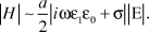
If we consider a lossless dielectric with ε2 = 0, we can obtain the order-of-magnitude relation between the electric energy

where ε0 is vacuum permittivity, and magnetic energy

where μ is magnetic permeability as U M/U E ∼ (πna/λ)2. Thus the magnetic field energy is much smaller than the electric field energy. This is, of course, the well-known quasi-static limit stating that the magnetic field is negligibly small if the electric field is confined on sub-λ scales. What does this mean from the energy conservation point of view? In a normal electromagnetic mode, the energy is stored for one quarter of the period T opt in the form of electrical (“potential”) energy U E (Figure 1a), and the other quarter of the period is in the form of magnetic (“kinetic”) energy U M (Figure 1b). For a resonator with dimensions larger than half λ, it is possible to have U E = U M, and thus the energy can remain confined indefinitely, oscillating between the magnetic and electric forms. However, for subwavelength resonators, the energy cannot remain inside the volume and will naturally radiate. This is the diffraction limit in the perfect dielectric medium.
But another component of energy has not been included in our model so far—the kinetic energy of motion of charged carriers moving under the influence of the electric field, U K.Reference Urzhumov and Shvets24 Since oscillations of the velocity of the carriers are shifted 90 degrees relative to the electric field, the kinetic energy adds to the magnetic energy (Figure 1b), and when the energy conservation gets restored (i.e., U K + U M = U E), self-sustaining oscillations of the mode become possible. Now, the kinetic energy becomes large only if the carriers are free (as in metals and other conductors), or if the ions are driven past their resonance frequency (in polar insulators and semiconductors), both characterized by negative dielectric permittivity. At this point, we shall concentrate on metals since their permittivity remains negative well into the visible range, while ionic resonances typically occur only in the mid-IR (infrared) and far-IR range.
We then conclude that the only manner in which sub-λ confinement can be achieved in the optical or near-IR range is through coupling the electric field with the kinetic motion of free carriers, which is the definition of the surface plasmon polariton (SPP). It is quite common to relate the kinetic energy of charged carriers to the electric current I as U K = L KI 2/2, where L K is the so-called kinetic inductance.Reference Day, LeDuc, Mazin, Vayonakis and Zmuidzinas25 This inductance has nothing to do with the magnetic fields and is simply the measure of the electron’s inertia in the metal. The kinetic inductance of a wire of length l and cross-section S can be found as

where m is the mass of electrons, e is electron charge, and N is their density. The most important property of the kinetic inductance is that it becomes very large for small cross-sections. In fact, a rapid rise of kinetic inductance has been shown to be the main cause preventing MMs from operating at high optical frequencies.Reference Zhou, Koschny, Kafesaki, Economou, Pendry and Soukoulis26, Reference Klein, Enkrich, Wegener, Soukoulis and Linden27 But this rise of kinetic inductance also has serious implications for loss in plasmonics and MMs.
Why the loss does not depend on shape
In the limit of a very small mode, one half of the time, all of the energy is stored in the form of kinetic energy of the electrons. The kinetic motion of electrons is characterized by the rate at which their velocity is damped, γm, which is determined by many different scattering processes, explained in detail in the following sections, and is a function of the frequency ω. The damping rate enters the expression for the metal’s dielectric function,

where εib is the dielectric constant due to the interband transitions, discussed later in the text, and, as mentioned previously, γm is on the order of 1014 s–1 for typical noble metals. If the velocity is damped with the rate γm, then the kinetic energy is dissipated at twice that rate (i.e., 2γm). And since, on average, energy is contained half of the time inside the metal in the form of kinetic energy, the total energy of the subwavelength mode decays at a rate that is not that different from γm. What is most striking about this simple resultReference Khurgin and Sun23, Reference Wang and Shen29 confirmed by many studies, is that the loss depends on neither the exact shape nor exact size of the structure, as long as the structure remains substantially subwavelength in all three dimensions.
Consider the two cases shown in Figure 2: silver (Figure 2a) and gold (Figure 2b) spheroids embedded in a semiconductor (InGaAs) and having resonance at the telecommunication wavelength of 1300 nm. As shown,Reference Khurgin and Sun28 while the dimensions of the spheroid remain less than 80 nm (corresponding to roughly λ/4n), the nonradiative energy dissipation rate γnrad remains near γm In addition to the nonradiative rate, there is also a radiative loss channel; however, it remains relatively small for the small spheroids. Numerous simulations of diverse geometries, all yield essentially the same result: once the physical dimensions of the structure become significantly less than the wavelength, the energy loss is always determined by energy loss in the metal and is independent of shape and size.Reference Khurgin and Sun23, Reference Wang and Shen29 Hence any attempt to reduce the loss by engineering a special shape of the subwavelength mode would be futile.
Decay rates of surface plasmon modes of (a) silver and (b) gold spheroids resonant at 1300 nm as a function of the size. Note that decay is dominated by the nonradiative energy dissipation rate γnrad, rather than radiative energy dissipation rate γrad, and the total decay rate exhibits very weak dependence on size. Adapted from Reference 28.

Why are the losses small in THz/microwaves but high in visible/near-IR?
From the previous discussion, it follows that any sub-λ structure is very lossy, since a significant fraction of the energy has to reside inside the metal, where it is rapidly dissipated. But consider the familiar example of a solenoid in a transformer operating at an ac frequency of 50 Hz. Considering its low frequency of operation (and therefore a wavelength ∼1000s of km), such a device is clearly subwavelength in all three directions; however, it operates with remarkable efficiency. Clearly, the conclusions of inevitably high loss in a subwavelength structure only hold for high frequencies. This result can be understood if one notes that at low frequencies in metallic structures, conductivity current dominates the displacement current, and Maxwell’s equation can be written as ∇×H = σE, leading to the familiar result for the field magnitudes. Notice that the magnetic field depends on the size of the metallic object but not on the wavelength. If conductivity is sufficiently high, the magnetic field energy can be sufficient to store all the energy of the oscillating mode. The boundary between “high” or optical frequencies dominated by displacement current and “low” or “RF” frequencies dominated by the conductivity current lies where the angular frequency equals the dissipation rate in the metal (i.e., ω = γm. For the typical values of γm, this “border” between optics and electronics lies around 5–10 THz (λ = 30–60 μm), hence at frequencies below 5–10 THz, very low loss subwavelength structures become feasible, as demonstrated by numerous groups working in the range from 10 GHz to a few THz.Reference Smith, Padilla, Vier, Nemat-Nasser and Schultz30–Reference Padilla, Taylor, Highstrete, Lee and Averitt32 It is rather ironic that in this low frequency range, where the quality (Q)-factor of the metal itself, Q m = ω/γm, is quite small (less than unity), one can engineer resonance structures such as split-ring resonators with a very high Q-factor Qr = ω/γnrad.
To summarize this section, one can only achieve sub-λ confinement by introducing a material with a negative real component of its dielectric constant. Then, if the confinement is significantly sub-λ in all dimensions, and the angular frequency is higher than the metal scattering rate γm, roughly one half of the energy resides in kinetic motion of electrons in the metal, and thus the energy dissipation rate is close to γm. No amount of tinkering with the shape of the structure will yield a reduction of loss.
One can depict what is happening using the graphical representation shown in Figure 3. Here the logarithmic horizontal axis represents the wavelength in the material, and the logarithmic vertical axis represents confinement at characteristic size a. A 45-degree inclined a = λ/n line separates the subwavelength region below the line from the larger-than-the wavelength region above the line. A vertical line passing near λ = 50 μm (6 THz frequency) separates the region where the displacement current dominates (left) from the region where the conductivity current dominates (right). One can identify the regions for optics (dominated by reactive current with features >λ), electronics (dominated by the conductivity current with features <λ), and plasmonics (dominated by reactive current with features <λ). Both optical and electronic regimes can have very low loss, but the plasmonic regime is always inherently lossy, as long as the metals used are intrinsically lossy. Once one accepts this inevitable fact of life, it pays to consider the nature of absorption in metals and other materials with free carriers to ascertain what can be done to lessen the intrinsic loss.
Diagram explaining three different regimes for electromagnetic waves: electronics (low frequency, subwavelength), optics (high frequency, larger than a wavelength), and plasmonics (high frequency, subwavelength, and inherently high loss). n, index of refraction; a, characteristic length; λ, wavelength; ω, frequency; and γm metal damping rate.

Why and how do metals absorb and reflect light?
Venturing beyond the Drude model
According to the Drude theory,Reference Ashcroft and Mermin21 developed in 19th century and based on describing electric current as the flow of the electron gas, the loss, represented by the imaginary part of the dielectric constant  is associated with the scattering of conduction electrons by defects, surface states, and lattice vibrations. Consequently, the most apparent path toward reduced loss is improving the quality of the metal to avoid defects, but this method does not reduce scattering by lattice vibrations. The latter can be only partially mitigated by lowering the temperature, and having practical devices operating at cryogenic temperatures is hardly an option. Furthermore, in small nanoparticles, there is always a disproportionate contribution to the loss by surface states that is difficult to reduce. What is implicitly assumed by Drude theory is that the scattering rate γm does not have frequency dependence, and hence, if the material happens to be a good conductor at relatively low RF, it should also be a good plasmonic material. However, the reality is quite different—a good conductor is not necessarily a good plasmonic material. For instance, the conductivity of copper is almost twice that of aluminum, but the latter has significantly lower loss in the optical range and can be used in plasmonics, while copper has a much higher loss in the optical range.Reference Palik33
Clearly, the scattering rate is different at different frequencies and should be related to the intricacies of the band structure of the material. Consider the simplified band structure of a typical noble metal such as goldReference Christensen and Seraphin34 shown in Figure 4a. The main band responsible for the electrical conductivity is the partially occupied conduction band formed by hybridized outer s and p shells of gold. The Fermi surface separates filled electron states from unoccupied ones. According to the standard conductivity description, when an external field is applied to the material, the Fermi surface shifts, and electrical current flows. The key feature of conduction at relatively low frequencies is that only the states that are very close to the Fermi surface participate in conduction, and the resistivity is determined only by the density of states (DOS) near the Fermi surface and the scattering rate between them.
Absorption in metals. (a) Simplified energy band diagram of a noble metal with an intraband free carrier absorption (red arrows) and interband absorption (blue arrows). On the right side, absorption of a low energy photon requires simultaneous absorption of a phonon. On the left side, absorption of higher energy photon can be accompanied by either absorption or emission of a phonon. (b) Spectrum of imaginary part of dielectric constant ε2 and absorption. k, wavevector; ħ, reduced Planck’s constant; ω, frequency; ωB, frequency at the interband absorption edge; ω1, ω2, ω3, increasing values of the frequency; and θD, Debye frequency.

From the quantum mechanical point of view, the energy of the material interacting with an electromagnetic field of frequency ω can only be changed in increments of ħω, and the loss mechanism is described as absorption of the photons. The process of absorption involves transitions from filled states below the Fermi level to the unoccupied states above the Fermi level, as shown in Figure 4a. Since the momenta ħk of the two states are different, an additional scattering mechanism must be involved. The scattering can be either by lattice vibrations (phonons), surface imperfections, impurities, or additional electrons excited from below the Fermi level. As long as the frequency remains relatively small (ω1 in Figure 4a), the absorption is determined entirely by the DOS and scattering strength near the Fermi surface, as in standard conductivity theory.
As one increases the frequency to higher values ω2, more states get involved in absorption, and the absorption can no longer be described only by properties near the Fermi surface—the whole conduction band now participates. Furthermore, as the frequency increases, a whole new set of states gets involved. Such states are in the bands containing the d-shell electrons and lie below the Fermi level overlapping with the main s-p conduction band. As the photon energy increases to a certain “interband edge” value ħωB (1.74 eV for Au), electrons start making transitions from the d-band states to unoccupied states in the main conduction band as shown in Figure 4. These transitions are direct (vertical) interband transitions in which the momenta of initial and final states are equal, and no additional scattering is required. Furthermore, the d-band is relatively narrow and has a large DOS. Therefore the interband transitions are very strong, and the metals become strong absorbers at higher frequencies. As frequency keeps increasing to still higher values (ω3) additional interband transitions from the main conduction band to the higher conduction bands also become a factor, and absorption increases even further.
Thus the absorption (imaginary part of permittivity ε2) at optical frequencies is determined by many states at different energies and has two components—an intraband component due to free electrons in the s-p band and the interband component due to direct transitions between the bands. The free electron component loosely follows the Drude formula 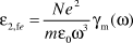 but with a frequency-dependent scattering rate, γm(ω), while the interband component ε2,ib behaves more like the ε2 of a semiconductor—it is very low below ωB and very high above, as shown in Figure 4b. In order to operate with lower loss, one has to operate at frequencies less than ωB, but even in this region, the loss is determined by the states throughout the conduction band and not just the states on the Fermi surface.
And what about the real part of permittivity, ε1, responsible for reflection and refraction? Since no energy is being transferred to the metal, the transitions contributing to ε1 are the so-called virtual transitions with a photon attempting to “push” the electron into the higher state but not having sufficient energy to do so. The electron thus ends up where it started, at the same energy level. According to the Pauli principle, such transitions are allowed only if the state is partially occupied (i.e., lies very close to the Fermi surface), just as in standard conductivity theory. Therefore, the real part of permittivity due to free electrons is very well described by the Drude formula. Overall, for frequencies below the absorption edge, one can always fit experimentally measured values of the dielectric constant into the modified Drude formula,

where εib is the contribution of interband transitions, but it is very important to take into account that the scattering rate can have a very complicated frequency dependence.
Can the loss be reduced by cooling?
It is known that the dc resistivity of metals decreases drastically as the temperature gets lower. According to Matthiessen’s rule, the resistivity of the metal is described as ρ(T) = a RT+ ρR, where the temperature coefficient a R is due to phonon scattering, and ρR is the residual resistivity due to surface imperfections and impurities. For a reasonably pure material, the resistivity indeed becomes very low at cryogenic temperatures. However, when one considers resistivity (i.e., absorption) at optical frequencies, the residual resistivity stays quite high, and it cannot be reduced, regardless of how much the temperature is reduced.Reference Liu, Pelton and Guyot-Sionnest35–Reference Parkins, Lawrence and Christy37
The explanation for the large difference between low temperature conductivities at low and high frequency can be seen in Figure 4a. The strongest scattering process required for indirect intraband processes shown is absorption and emission of phonons. If the energy of a photon is less than the energy of the average acoustic phonon, the so-called Debye energy ħθD, which is ∼15–20 meV for noble metals, the emission of a phonon is not allowed, since it would require the electron to end up in an already occupied state below the Fermi level, which is forbidden by Pauli’s Principle. The absorption of the phonon is allowed, but the number of phonons decreases with decreasing temperature and thereby causing a reduction in the scattering rate γm.
When the photons have energy higher than ħθD, there is enough energy to allow the phonon emission as well as absorption, as shown on the left-hand side of Figure 4a.Reference Lawrence and Wilkins38 Of course one does not need one phonon to emit another phonon spontaneously, hence even at absolute zero, phonon scattering remains strong, and the scattering rate γm does not get reduced significantly from its value at room temperature. In addition to phonon scattering, the absorption at optical frequencies can be aided by the electron-electron scattering,Reference Parkins, Lawrence and Christy37–Reference Gurzhi39 which has a large temperature-independent contribution.
Interestingly, the Debye frequency θD that separates the “high frequency” region from the “low frequency region” is about 5–10 THz, such that in the THz region and below, the cooling will cause a substantial reduction of already relatively low loss, but for the near-IR and optical regions, the cooling will not reduce the loss substantially.
The role of the density of states
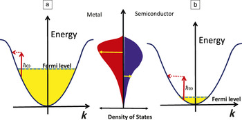
Having established the fact that the loss at optical frequencies depends on the DOS and the strength of the interaction between electrons, phonons, and impurities, it is logical to ask the question: What is the defining factor behind the loss? The strength of interaction for various processes does not change significantly as a function of energy inside the band, and even from one material to another, but the DOS into which the scattering can take place can vary by many orders of magnitude. The main reason explaining why the scattering of carriers in metals occurs on a very short (femtoseconds) time scale is that there is always a large number of empty states in the conduction band above the Fermi level ready to accept the scattered carriers, as shown in Figure 5a. Of course, the DOS available for scattering is large because the density of free carriers is high, and thus the Fermi level is high in the conduction band.
Band diagram and density of states of a (a) metal and (b) a highly doped semiconductor. Lower density of states in the semiconductor is responsible for the reduced loss. k, wavevector; ħ, reduced Planck’s constant; and ω, frequency.

Therefore, the best chance to reduce absorption in the metal is to reduce the DOS available for scattering, as for example, in highly doped semiconductors shown in Figure 5b. In this case, since the carrier density is relatively low, the Fermi level stays close to the bottom of the conduction band and the DOS available for scattering is substantially lower than in the metals. Indeed the scattering times in semiconductors are usually on the scale of 100 ps (i.e., a few times longer than in the noble metals). Of course, the decrease in the scattering rate is a consequence of reduced carrier density, and there is a reduction in the plasma frequency and therefore an inability to achieve resonance in the visible range. But as shown in subsequent sections, one can attain reduced absorption in the all-important near-IR range.
To summarize this section, rigorous treatment of absorption at optical frequencies beyond the Drude approximation in metals shows that the main factor defining the strength of absorption is the DOS available for scattered carriers. Therefore, one should look for materials with reduced DOS into which the scattering can take place. The search for these materials is the subject of the next two sections.
Alternative materials survey
The search for alternative plasmonic materials with improved optical properties over traditional materials such as silver and gold could ultimately lead to long-awaited, real-life applications of plasmonic devices and MMs.Reference Boltasseva and Atwater15 This requires that we turn away from the conventional approach of using only noble metals and look into different materials and compounds. Looking at other metals does not bring any surprises. While metals other than silver and gold have been used in plasmonics, their use is very limited, as their losses are even higher than in noble metals. Nickel, platinum, and palladium can be used for specific plasmonic applications where the usage of lossy metals can be justified by the required functionality (for example, chemiluminescence or catalytic activity) (see Reference Reference West, Ishii, Naik, Emani, Shalaev and Boltasseva16 and references therein). Among the alkali metals, sodium and potassium are expected to have the lowest lossesReference Palik40, Reference Blaber, Arnold, Harris, Ford and Cortie41 but their extreme reactivities have made the fabrication of alkali metal structures prohibitive. Copper would be a good candidate to replace silver and gold as a plasmonic material, but fabricating devices with copper is challenging, as it easily oxidizes.Reference Chan, Zhao, Hicks, Schatz and Van Labeke42 Aluminum has not been an attractive plasmonic material due to the existence of an interband transition around 800 nm, but it can still be used as a plasmonic material in the blue and UV range.Reference Langhammer, Schwind, Kasemo and Zoric43 Thus, in the search for better plasmonic materials, one should aim at studying different material classes as well as adjusting/improving the optical properties of existing metallic materials via doping, alloying, and careful band-structure engineering.Reference West, Ishii, Naik, Emani, Shalaev and Boltasseva16, Reference Blaber, Arnold and Ford44, Reference Bobb, Zhu, Mayy, Gavrilenko, Mead, Gavrilenko and Noginov45
Metallic alloys, intermetallics, and metallic compounds have been considered as potential candidates for alternative plasmonic materials (see Reference Reference West, Ishii, Naik, Emani, Shalaev and Boltasseva16 and references therein). By alloying two or more elements, one can, to some degree, change optical characteristics of metals to create band structures that can be fine-tuned by adjusting the proportion of each alloyed material.Reference Bobb, Zhu, Mayy, Gavrilenko, Mead, Gavrilenko and Noginov45 While many alkali-noble metal compounds have been presented as alternative plasmonic materials, they cannot be used for applications in the optical range.Reference West, Ishii, Naik, Emani, Shalaev and Boltasseva16, Reference Blaber, Arnold and Ford44
The search for different materials is also driven by yet another important issue associated with the usage of silver and gold. Aside from high losses, another problem with noble metals is that their real part of the dielectric permittivity cannot be tuned/adjusted and is often too large to be useful in many MM and TO applications,Reference West, Ishii, Naik, Emani, Shalaev and Boltasseva16 specifically for devices such as hyperlenses or epsilon-near-zero materials (materials with the real part of their effective dielectric permittivity going to zero at the optical frequency) that enable subwavelength resolution imaging or directional beaming, respectively.Reference Jacob, Alekseyev and Narimanov46, Reference Engheta47 TO applications typically require that the polarization responses of the dielectric and metallic components should nearly balance. This would require that the magnitudes of their real permittivities should be similar, but noble metals have very high carrier densities, making their real permittivities very large. Yet more crucial is that the optical properties of metals are not tunable, and hence many plasmonic applications that require switching or modulation would be challenging to realize with the use of metals. Finally, noble metals are not compatible with standard silicon nanofabrication technology and cannot be easily integrated into standard silicon processes.
Many of the drawbacks of noble metals can be overcome with the use of other non-metallic materials. Recent studies have now expanded the possibilities beyond gold and silver to a variety of materials exhibiting superior behavior for different applications at different frequencies.Reference Boltasseva and Atwater15, Reference West, Ishii, Naik, Emani, Shalaev and Boltasseva16 It was shown that the available choices for a particular wavelength range depend on the carrier concentration achievable in the material and the optical losses (Figure 6).Reference Boltasseva and Atwater15, Reference West, Ishii, Naik, Emani, Shalaev and Boltasseva16 In Figure 6, various classes of materials are grouped using two important parameters that determine the optical properties of conducting materials: the carrier concentration and carrier mobility. In plasmonics, the carrier concentration has to be high enough to provide a negative real part of the dielectric permittivity, but it is also desirable for it to be tunable so that different dielectric permittivity values would be accessible with changes in carrier concentration. Lower carrier mobilities could indicate higher Drude damping losses and thus higher material losses. Of course, additional losses due to interband transitions (as highlighted in Figure 7) are highly undesirable. The ideal material for plasmonics would lie at the left end of the plot on the horizontal plane where interband losses are zero. Such a lossless metal is, however, still elusive.Reference Khurgin and Sun48
Material space for plasmonics and metamaterial applications. Important material parameters such as carrier concentration (maximum doping concentration for semiconductors), carrier mobility, and interband losses form the optimization phase space for various applications. While spherical bubbles represent materials with low interband losses, elliptical bubbles represent those with larger interband losses in the corresponding part of the electromagnetic spectrum.Reference Boltasseva and Atwater15

Density of states histograms (spin included) of TiN near the Fermi level are lower than that of a metal, compared with Figure 6 (adapted from Reference Reference Ern and Switendick55). Shaded region represents filled bands.

Promising candidates to replace noble metals in plasmonics and optical MMs include transparent conducting oxides (TCOs),Reference West, Ishii, Naik, Emani, Shalaev and Boltasseva16, Reference Rhodes, Franzen, Maria, Losego, Leonard, Laughlin, Duscher and Weibel49–Reference Noginov, Gu, Livenere, Zhu, Pradhan, Mundle, Bahoura, Barnakov and Podolskiy51 transition-metal nitrides,Reference Naik, Schroeder, Ni, Kildishev, Sands and Boltasseva52 and transition-metal dioxide compounds.Reference Wang, Clavero, Yang, Radue, Simons, Novikova and Lukaszew53 One could classify alternative plasmonic materials in the near-IR and visible ranges into categories of semiconductor-basedReference West, Ishii, Naik, Emani, Shalaev and Boltasseva16 and ceramics.Reference Naik, Kim and Boltasseva50 In the search for better plasmonic materials, TCOs were proposed as low loss alternatives to gold and silver in the near-IR range.Reference West, Ishii, Naik, Emani, Shalaev and Boltasseva16, Reference Naik, Kim and Boltasseva50, Reference Noginov, Gu, Livenere, Zhu, Pradhan, Mundle, Bahoura, Barnakov and Podolskiy51 However, TCOs cannot be plasmonic (i.e., exhibiting metallic properties) at visible wavelengths because the carrier concentration is limited to around 1021 cm−3.Reference Minami54 In contrast, transition metal nitrides are ceramics whose carrier concentrations can reach 1022 cm–3 and can be good plasmonic materials in the visible range.Reference Naik, Kim and Boltasseva50 As TCOs, these materials are compatible with semiconductor manufacturing processes and have properties that can be changed significantly by changing the deposition conditions.
A generalized approach to the discovery of a good plasmonic material could be outlined as follows: Since the losses associated with metals partly arise from free-electron densities that are too large, one could either reduce carrier density in metals or increase it in semiconductors to the desired value. In materials with intermediate carrier concentrations such as titanium nitride, the Fermi level stays close to the bottom of the conduction band, and the DOS available for scattering is lower than in metals (see Figure 7 adapted from Reference Reference Ern and Switendick55).
Graphene is another material that has generated excitement due to its unique band structure and high carrier mobility.Reference Jablan, Buljan and Soljacic56–Reference Geim and Novoselov58 The 2D carrier density in a graphene sheet is of the order of 1011–1013 cm–2, and can be electrically controlled by an applied gate voltage. This offers an exciting possibility of tunable surface plasmon polaritons at mid-IR frequencies.Reference Jablan, Buljan and Soljacic56 Recently, impressive localization for SPs propagating in graphene was predicted,Reference Koppens, Chang and García de Abajo57 and the first demonstrations of graphene plasmons at terahertz wavelengths were reported.Reference Ju, Geng, Horng, Girit, Martin, Hao, Bechtel, Liang, Zettl, Shen and Wang59
With the rapid development of the plasmonic materials field, it is clear that there will not be a single plasmonic material that is suitable for all applications at all frequencies.Reference West, Ishii, Naik, Emani, Shalaev and Boltasseva16 Rather, a variety of material combinations must be tuned and optimized for specific applications.Reference West, Ishii, Naik, Emani, Shalaev and Boltasseva16, Reference Naik and Boltasseva60–Reference Tassin, Koschny, Kafesaki and Soukoulis63 Different plasmonic, MM, and TO devices have different requirements for high performance,Reference West, Ishii, Naik, Emani, Shalaev and Boltasseva16, Reference Naik and Boltasseva61 and hence they suggest different materials as their best choice. One example is aluminum-doped zinc oxide that performs poorly compared to noble metals for surface plasmon waveguiding but greatly outperforms silver in the realization of hyperbolic MMs—a class of MMs, which are useful for far-field subwavelength imaging and exhibit negative refraction and broadband singularity in the photonic density of states, quite unlike conventional photonic systems.Reference Naik and Boltasseva61, Reference Naik, Liu, Kildishev, Shalaev and Boltasseva64 There are specific applications such as negative-index materials, where silver and gold remain the materials of choice.Reference Tassin, Koschny, Kafesaki and Soukoulis63 However, for many important applications such as hyperbolic MMs, epsilon-near-zero materials, tunable/switchable MMs, and TO devices, alternative plasmonic materials provide both needed functionalities as well as modulation capability and ease of fabrication and integration. Alternative plasmonic materials thus have the potential to make an enormous impact on both optics and nanoelectronics by allowing for a new generation of unparalleled device applications.
Experiments with semiconductors and ceramics
Transparent conducting oxides
Normally semiconductors behave as dielectrics at frequencies above several hundred THz, but they can also exhibit a negative real permittivity in this spectral region.Reference Hoffman, Alekseyev, Howard, Franz, Wasserman, Podolskiy, Narimanov, Sivco and Gmachl65 Due to the ease of fabrication and flexibility in tuning their properties, semiconductors are very attractive candidates for plasmonic materials. To target low-loss plasmonic behavior, the bandgap and plasma frequency of the semiconductor both must be larger than the frequency range of interest such that we achieve both a negative real permittivity and no interband transition losses. Despite the abundance of semiconductors with large bandgap values (>1.5 eV) and high carrier mobilities, very high doping levels are necessary to bring the crossover frequency of semiconductors into the optical range.
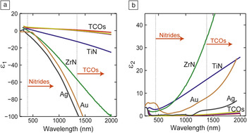
Plasmonic and MM applications in the near-IR range require high doping that can be achieved in heavily doped oxide semiconductors. Such ultrahigh doping—up to about 1021 cm–3—can be obtained in TCOs, making them good candidates for near-IR plasmonics.Reference West, Ishii, Naik, Emani, Shalaev and Boltasseva16, Reference Naik, Kim and Boltasseva50, Reference Rhodes, Franzen, Maria, Losego, Leonard, Laughlin, Duscher and Weibel66 These include indium-tin-oxide (ITO) and zinc oxide doped with aluminum (AZO) or gallium (GZO).Reference Naik, Kim and Boltasseva50 These TCOs can be easily deposited by many techniques such as pulsed laser deposition, sputtering, and atomic layer deposition.Reference Frölich and Wegener67 It has been shown that ITO and GZO films exhibit metallic properties for wavelengths >1.3 μm, while AZO shows metallic properties for wavelengths >1.8 μm. The material losses in TCOs are about four times smaller than those in silver at similar near-IR wavelengths (Figure 8).
Comparison of optical properties of alternative plasmonic materials with those of conventional metals. Optical constants of low loss thin films of TiN, ZrN, and transparent conducting oxides (TCOs) (AZO, zinc oxide doped with aluminum; GZO, zinc oxide doped with gallium; and ITO, indium tin oxide) are plotted along with those of gold and silver. The arrows show the wavelength ranges in which nitrides and TCOs are, respectively, metallic. Panel (a) shows that TCOs and nitrides have smaller negative permittivity values than those of metals, while (b) compares losses and shows that losses in TCOs are many times smaller than those in either gold or silver. The losses in nitrides are slightly higher than in metals due to interband transitions at the crossover frequency. Dielectric functions of thin films were obtained using spectroscopic ellipsometry. ε1, real part of the dielectric constant; ε2, imaginary part of the dielectric constant.Reference Naik, Kim and Boltasseva50

Transition-metal nitrides
Among the many transition-metal nitrides, non-stoichiometric nitrides of Ti, Hf, Zr, and Ta have been studied as potential plasmonic materials.Reference Naik, Kim and Boltasseva50 The optical dielectric functions for TiN and ZrN films are shown in Figure 8 together with those of noble metals and the previously mentioned TCOs. The nitride films of TiN and ZrN are metallic for wavelengths >500 nm. The losses can be lowered by further optimization of deposition conditions and substrate choice.Reference Naik, Kim and Boltasseva50 For example, substrates such as sapphire and MgO provide lattice matching for TiN films and promote epitaxial growth, leading to crystalline films and thereby reducing optical losses.Reference Naik, Schroeder, Ni, Kildishev, Sands and Boltasseva52
Performance of TiN can be comparable to that of gold for plasmonic applications and can outperform gold and silver for some MM applications in the visible and near-IR regions.Reference Naik, Schroeder, Ni, Kildishev, Sands and Boltasseva52, Reference Guler, Naik, Boltasseva, Shalaev and Kildishev62
When considered for plasmonic applications, TiN and TCO nanoparticles enable strong localized surface plasmon resonances (LSPR) in the red end of the visible and in the near-IR ranges, respectively.Reference Guler, Naik, Boltasseva, Shalaev and Kildishev62 TiN and ZrN could also be promising substitutes for metals for SP waveguiding applications.Reference Naik, Schroeder, Ni, Kildishev, Sands and Boltasseva52 Both TCOs and transition-metal nitrides outperform gold and silver by many orders of magnitude for non-resonant MMs such as hyperbolic MMs.Reference Naik, Schroeder, Ni, Kildishev, Sands and Boltasseva52, Reference Naik and Boltasseva61 Tunable/adjustable optical properties of these materials combined with easier fabrication, and integration makes transparent conducting oxides and transition-metal nitrides very promising candidates for novel, low-loss, and tunable plasmonic devices.
To summarize this section, transparent conducting oxides and transition metal nitrides such as TiN are good replacements for noble metals as plasmonic elements in the optical range for many plasmonic and MM applications.
Can the gain compensate the loss?
Plasmonic amplifiers and SPASERs
Having established the near-inevitability of having significant loss in any plasmonic structure with sub-λ confinement in all three dimensions and recognizing that this loss cannot be easily engineered away, the next logical step would be an attempt to compensate this loss with optical gain. That would not only allow one to have efficient plasmonic interconnects and devices and low-loss MM structures,Reference Noginov, Podolskiy, Zhu, Mayy, Bahoura, Adegoke, Ritzo and Reynolds68 but also would engender miniature sub-λ sources of coherent radiation, or SPASERs. Research in this area has been given a great impetus by a seminal proposal by Bergman et al.Reference Bergman and Stockman69 for a coherent generator of SPs (SPASER) consisting of a metal nanoparticle surrounded by a semiconductor gain material. The first estimate given in that work has shown that the population inversion required to compensate the loss in the metal was realistic. Since then, a multi-pronged effort, both theoreticalReference Stockman70–Reference Lu and Chuang74 and experimentalReference Noginov, Zhu, Belgrave, Bakker, Shalaev, Narimanov, Stout, Herz, Suteewong and Wiesner75–Reference Leon and Berini89 devoted to spasing has blossomed, and yet, there has been but a single demonstration of “laser-like” behavior in gold-dye media consisting of a line-width narrowing and somewhat nonlinear output behavior under intense pulsed optical pumping.Reference Noginov, Zhu, Belgrave, Bakker, Shalaev, Narimanov, Stout, Herz, Suteewong and Wiesner75 When it comes to developing a practical semiconductor SPASER, a great number of diverse schemes has been successfully demonstrated, including mostly optical but also injectionReference Ding, Liu, Yin, Hill, Marell, van Veldhoven, Nöetzel and Ning78 pumping. Various geometries, such as nanowires,Reference Oulton, Sorger, Zentgraf, Ma, Gladden, Dai, Bartal and Zhang76 double heterostructure mesas,Reference Hill, Marell, Leong, Smalbrugge, Zhu, Sun, van Veldhoven, Geluk, Karouta, Oei, Nötzel, Ning and Smit77, Reference Ding, Liu, Yin, Hill, Marell, van Veldhoven, Nöetzel and Ning78 disc structures,Reference Kwon, Kang, Seassal, Kim, Regreny, Lee, Lieber and Park79 nanopatches,Reference Lakhani, Kim, Lau and Wu80 and coaxial pillarsReference Lee, Khajavikhan, Simic, Gu, Bondarenko, Slutsky, Nezhad and Fainman81–Reference Khajavikhan, Simic, Katz, Lee, Slutsky, Mizrahi, Lomakin and Fainman83 have been used, but they all have one feature in common; in all of them, the device is larger than a wavelength in the material in at least one dimension. The threshold has been universally high, and with a few exceptions, the pumping was either optical or required low temperature. A number of reviewsReference Stockman70, Reference Stockman71, Reference Oulton84–Reference Berini and Leon87 recently published confirm the fact that truly sub-λ electrically pumped SPASER is not currently on the horizon. As we have shown previously, in subwavelength plasmonic structures based on noble metals,Reference Wang and Shen29, Reference Khurgin and Sun23, Reference Khurgin and Sun90 the damping rate is always on the scale of γm∼1014 s–1. To compensate for such a strong energy loss mechanism, a material gain on the order of 103–104 cm–1 would be required. This value is quite high, yet it is not unattainable in typical semiconductor media with the injected carrier density of ∼1018 cm–3, which is routinely attained in semiconductor lasers. This discovery has prompted researchers to embark on a quest to first compensate the loss and eventually achieve spasing in subwavelength structures. Most of the early proposals neglected the fact that what matters is not just the value of the gain and carrier density associated with it, but the pumping current density required to maintain this carrier density. And due to the Purcell effect,Reference Purcell91 described in the next section, that density can quickly reach entirely unsustainable values in subwavelength structures.
Stimulated and spontaneous emission: Density of states, this time for light
As was established by Einstein in 1917, interaction between matter and an electromagnetic field consists of three components: absorption, stimulated emission, and spontaneous emission.Reference Purcell91 Consider for simplicity a semiconductor with the valence band being the ground state and the conduction band being the excited state. In the case of absorption, the energy of the absorbed incoming photon causes an upward transition of an electron from the valence to the conduction band, generating an electron in the conduction band and a hole in the valence band and obviously reducing the photon’s density. If the electrons and holes have been injected into the semiconductor, they can recombine with (radiatively) or without (non-radiatively) the emission of a photon. Radiative recombination has two components—spontaneous and stimulated. Stimulated emission is the exact opposite of absorption—the electron-hole pair recombines and emits a photon that is as coherent (i.e., has the same phase, frequency, and polarization) as the incoming photons, thus increasing the photon density. When sufficient density of electron-hole pairs is injected, the probability of stimulated emission becomes higher than the probability of absorption, and the system provides optical gain that can potentially compensate the absorption in the metal. Unlike stimulated emission, spontaneous decay occurs independently of the incoming photons, and the emitted photon has random phase and direction of propagation.
As was shown by Einstein, the probabilities of stimulated and spontaneous emission are closely related, and in fact, the probability of spontaneous emission is proportional to the stimulated emission and to the density of photon states (i.e., number of modes into which the spontaneous emission can take place). In the unbounded dielectric medium, the DOS (per unit volume and unit frequency interval) is roughly Z 0 ∼ 8πλ−3ω−1. But once the field gets confined to the sub-λ mode with volume V, the DOS becomes larger, Z 1 ∼ 8πV −1∆ω, where Δω is the width of the mode. This is the Purcell effect according to which the spontaneous recombination rate is enhanced in comparison to the unbounded dielectric by the Purcell factorReference Purcell91FP ∼ Z 1/Z 0 ∼ (λ3/V)ω/∆ω. Our calculationsReference Khurgin and Sun23, Reference Khurgin and Sun90 show that either in localized SPP modes or in propagating short range (large wave vector) SPPs, the Purcell factor can easily exceed 100, which reduces the spontaneous recombination time t sp to a few tens of picoseconds or even less.
What are the implications of this giant Purcell enhancement? Quite simply, the carrier density N tran ∼ 5 × 1018 cm−3 required to compensate the loss in a metal-dielectric structure of characteristic dimension of a of approximately 50 nm necessitates the transparency current density of J tran = eN trana/t sp ∼ 5 × 10⁵A/cm2, which is about two orders of magnitude higher than the current density in a typical double heterojunction semiconductor laserReference Coldren and Corzine92 and is thus all but unattainable.
Compensation, but at what cost?
Consider a proposed metal-semiconductor-metal waveguide shown in Figure 9a designed to operate at the telecommunication wavelength of 1550 nm with an active layer of InGaAs of thickness d a sandwiched between two Ag layers that also act as contacts. The total thickness of the waveguide, including thin doped layers of InGaAlAs with a somewhat higher bandgap, is d. In Figure 9 (b–f), we plot characteristics of the device as a function of the waveguide thickness d.
(a) Metal-semiconductor-metal waveguide with loss compensation. (b–f) Characteristics of loss-compensated Ag/In0.53Ga0.47As/Ag plasmonic waveguide with gain operating at λ = 1550 nm as functions of thickness. d a, thickness of active layer; d, waveguide thickness; J, current density. Adapted from Reference Reference Khurgin and Sun90.

In Figure 9b, we plot the effective index neff, which is the ratio of the wavelength λS ∼440 nm in bulk InGaAs to the effective wavelength of the SSP propagating in the waveguide, λeff. As the waveguide thickness d decreases to 200 nm, or about λS/2, the effective index reaches 1.5 (i.e., the propagating mode becomes sub-λ in all dimensions).
Just as predicted by our order of magnitude analysis performed earlier in this article, once the mode becomes sub-λ, the modal loss approaches that of the metal damping rate γm, as shown in Figure 9c. In Figure 9d, we plot the density of electron-hole pairs required to fully compensate the loss as the transparency density N tran, which slowly grows toward 1019 cm–3 as the waveguide gets thinner. Such carrier densities are routinely achieved in high power heterojunction lasers, but in this subwavelength structure, we must take into account the Purcell factor, shown in Figure 9e, that rapidly grows as thickness d is reduced. As a result, the transparency current density J tran shown in Figure 9f increases rapidly and for d = 50 nm surpasses 100 kA/cm2 something barely achievable even in high power transistors. Such effective carrier injection densities can be achieved in principle using optical pulsed pumping,Reference Noginov, Podolskiy, Zhu, Mayy, Bahoura, Adegoke, Ritzo and Reynolds68, Reference Noginov, Zhu, Belgrave, Bakker, Shalaev, Narimanov, Stout, Herz, Suteewong and Wiesner75 but the practicality of such an arrangement, even ignoring the power dissipation issues, is uncertain.
Conclusions: Where do we go from here?
First, we have seen that in the optical and near-IR range, sub-λ confinement in all three dimensions inevitably leads to high loss commensurate with the loss in a pure metal. Therefore, if one can use disc-like and wire-like structures with at least one dimension being larger than a half-wavelength in the material, one should do so, and the losses will be reduced.
Second, we have observed that due to the Purcell effect, it is very difficult to achieve full compensation of the loss in the structures that are subwavelength in all three dimensions. It follows that an injection “SPASER”—source of coherent surface plasmon polaritons—is not practical. Once again, if possible, the structures that are larger than half-wavelength in at least one dimension are preferable. Also, one should note that while subwavelength sources of coherent SPPs are not likely to emerge, efficient injection sources of incoherent SPPs are quite feasible. In other words, instead of a SPASER, one may opt for a surface plasmon-emitting diode.
Third, we have learned that when one looks inside the mechanism of metal loss beyond Drude theory, one realizes that it is erroneous to think that the best conductors necessarily make the best plasmonic materials. We have seen that the main factor determining the loss is the density of final states in which the electron may end up after absorbing a photon. This opens exciting possibilities for synthesizing new materials combining negative permittivity with low lossReference Khurgin and Sun48 in the future and provides us with a sense of direction for searching through existing materials.
Fourth, it is anticipated that the extensive search for unconventional material building blocks instead of conventionally used noble metals will lead to significant progress in plasmonic and metamaterials devices. Alternative plasmonic materials, for example, transparent conducting oxides and transition-metal nitrides, could offer low loss compared to noble metals and in addition provide extraordinary tuning and modulation capabilities enabling novel switchable and complementary metal oxide semiconductor-compatible plasmonic devices. This nascent field is only just beginning and has the potential of transforming the whole field of plasmonic applications.
We hope that as more researchers join the quest for low loss negative permittivity materials, the problem of loss in plasmonics will be mitigated, and eventually eliminated, taking plasmonics out of the laboratory and into the everyday world.
Acknowledgments
J.K. acknowledges Princeton University, where he could spend a year away from his everyday routine, thinking of these problems. A.B. acknowledges support from the ONR MURI grant N00014–10–1-0942 and ARO grants 57981-PH and 57566-PH-RIP. We thank G. Naik, J. Kim, and N. Emani for help with preparation of the manuscript.