I. INTRODUCTION
High-power amplifiers (HPAs) that include GaN high-electron-mobility transistors (GaN HEMTs) have potential applications in radar systems, satellite communication systems, cellular base stations, etc. Efforts have been made to improve the performance of GaN field effect transistor (FETs) on the basis of the vast experience accumulated over the years [Reference Ohtsuka1–Reference Golio17]. While several high-power, high-efficiency HPAs have been reported in the past [Reference Ohtsuka1–Reference Takagi5], there is considerable scope for improvement of the HPA performance; this is because of the immaturity of the existing GaN technologies. Therefore, concurrent development of device and circuit design methods is desired. Empirical nonlinear circuit models (ENCMs) are widely used in circuit design. ENCMs are fast and converge well and give an accurate fit for DC and RF characteristics [Reference Curtice and Ettenberg6–Reference Deng9]. However, such circuit models are not suitable for use in device design because there is no explicit relationship between the model parameters and the device/physical parameters. Moreover, a relatively large number of parameters must be extracted. On the other hand, physical models involving device/physical parameter calculations are too slow to be used in circuit simulations; further, these models do not converge well during RF simulation because of the complicated and exhaustive calculation for some boundary regions [Reference Pedro10–Reference Staudinger, Golio, Woodin and de Baca13]. Therefore, simple ENCMs constructed using device/physical parameters are preferred. These models may help improve the device performance by contributing to an increase in the FET efficiency in practical circuit applications and facilitating device performance optimization in specific applications.
It is a widely accepted fact that hyperbolic tangent (tanh) functions can be used for a satisfactory description of the I–V and capacitance characteristics of HEMT devices [Reference Roblin, Kang and Morkoc15, Reference Roblin, Rohdin, Hung and Chiu16]. Such tanh functions have been used to describe the I–V characteristics of GaN HEMTs as well [Reference Angelov8, Reference Deng9]. The large-signal (LS) HEMT model [Reference Angelov, Bengtsson and Garcia7] is a highly accurate model whose convergence is sufficiently high for it to be used in circuit design simulation. However, the model parameters, as in the case of every empirical device model, are used for reproducing the shape of the I–V curves, gm, capacitance characteristics, etc., rather than for device design.
In this paper, we propose a new model based on ENCM equations designed using device/physical parameters. We modified the model to obtain a direct connection with the device/physical parameters. The model parameters are similar to the parameters used in device design. Furthermore, the number of model parameters for the nonlinear components (I ds, C gs, C gd) can be reduced to 17 because the same physical parameters are used to describe the I–V and capacitance characteristics. This model is extended to a GaN HEMT, and the model parameters are extracted; the modeled I–V and capacitance characteristics are in excellent agreement with the measurement results. Moreover, with this model, accurate determination of the S-parameters and LS RF characteristics is possible.
II. MODEL
A) Drain-current model
To construct a drain-current model, we started from the following physical equation:

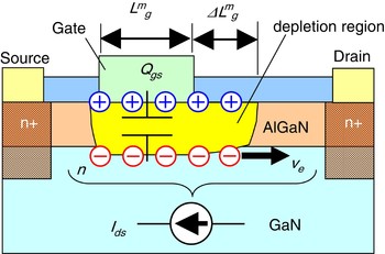
where I ds, q, n, and v e are the drain current, electron charge, electron concentration of the two-dimensional electron gas (2DEG) and electron velocity, respectively. Figure 1 shows a schematic cross section of an HEMT. The electrons with n and v e travel from the source to the drain in the channel.
Schematic cross section of HEMT model.

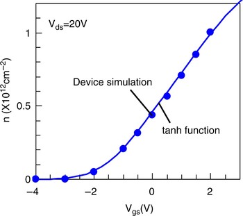
Next, we need to find a suitable function to model n and v e. It is known that n is controlled mainly by the gate voltage (V gs), and the tanh function was successfully used to model n = f(tanh(V gs)) [Reference Roblin, Kang and Morkoc15, Reference Roblin, Rohdin, Hung and Chiu16]. In order to make it possible to adjust the model for various cases, the tanh function for n was expressed as


where A, B, C 1, C 2, C 3, and D are constant. C 2 and C 3 are polynomial coefficients related to the carrier density.
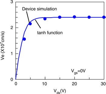
For v e, we adopted the following equation [Reference Ishihara and Shimizu18], which depends only on the drain voltage (V ds), that is, v e = g(tanh(V ds)), because the electron accelerates owing to the laterally electronic field between the gate and drain, as shown in Fig. 1:

where E and F are constants. We confirmed the effectiveness of equations (2)–(4) by technology computer aided design (TCAD) simulation, where we employed the 2D device simulator (Silvaco ATLAS [19]). Figures 2 and 3 show the curves of the tanh functions fitted to the TCAD simulation results. A, C 1, C 2, C 3, and D in equations (1) and (2) were 1.35e12 cm−2, 0.4 V−1, 0.0 V−2, 0.02 V−3, and 0.8 V, respectively. The values of E and F in equation (4) are 2.52e7 cm/s and 3.5 V, respectively. For both n and v e, the model using the tanh function agreed very well with the TCAD simulation results. Therefore, equations (2)–(4), which are designed on the basis of tanh functions, can be used to express the characteristics of n and v e.
Curve of tanh function fitted to TCAD simulation data for n.

Curve of tanh function fitted to TCAD simulation data for v e.

Finally, we represented the drain-current model by substituting equations (2)–(4) in equation (1) and assigning the parameters A–F to the device parameters:


where I max, V knee, V p, and g mpk are the maximum drain current, knee voltage, pinch-off voltage, and maximum transconductance, respectively. P 2 and P 3 are polynomial coefficients related to the carrier density and will allow us to adjust the current shape according to the channel profile. P 1 consists of two device parameters (I max, g mpk). Four of the input parameters (I max, V knee, V p, and g mpk) except P 2 and P 3 can be used as the device parameters, which are normally used in the device design and are familiar to the device engineers.
B) Capacitance model
The gate–source capacitance (C gs) model is constructed from the following physical-based equation:

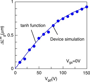
where Q gs and L mg are the gate charge and metallurgical-gate length, respectively. ΔL mg is defined as the extension length of the depletion region, as shown in Fig. 1. Usually, Q gs corresponds to the charge of the parallel plate with an effective gate length L mg. However, an extension of the depletion region from the gate edge to the drain should be considered, because a large V gd was applied to the GaN HEMTs. We consider an extension of the depletion region, expanding L mg to (L mg + ΔL mg). We used the tanh function, which limits the maximum value to ΔL mg, represented by

where G and H are constants. ΔL mg depends only on V gd, because the depletion region extends mainly laterally. The shape of the ΔL mg–V gd curve obtained by the TCAD simulation can be fitted well by equation (9), as shown in Fig. 4. G and H are 1.05 µm and 110 V, respectively. For n in equation (8), the same expression as that for n in the drain-current model in equation (5) can be used. This reduces the number of model parameters.
Curve of the tanh function fitted to TCAD simulation data for ΔL mg.

Finally, the model C gs is represented by

where C gs0, R Lg, αLg, and C gspi are the gate–source capacitance, the ratio of L mg + ΔL mg to L mg, gate extension coefficient, and the parasitic capacitance between gate and source, respectively.
In the case of the gate–drain capacitance (C gd), the charge model (Q gs) is not sufficient to produce a useful C gd expression from the physics. Because the C gd is smaller than one-tenth of C gs, and more accuracy model of the Q gs is necessary. So we used the conventional expression of the inversely proportional function dependent only on V gd [Reference Staudinger, Golio, Woodin and de Baca13] instead, which yields

where V bi, C gdpi, and MSCGD are the built-in voltage, parasitic capacitance, and capacitance coefficient for C gd, respectively. C gd0 is the gate–drain capacitance at V gd = 0.
C) Relationship between model parameters and physical parameters
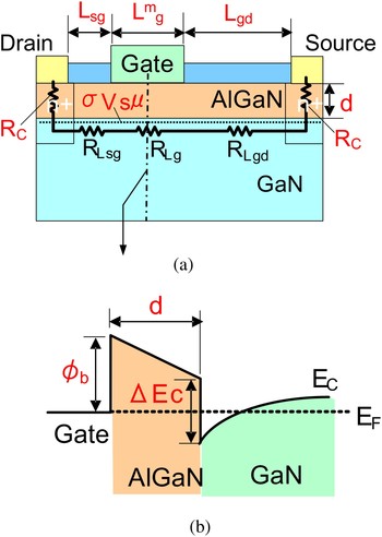
Figures 5(a) and 5(b) show the device structure for GaN HEMTs and the band diagram under the gate electrode. In Fig. 5(a), L sg and L gd are the gate–source distance and the gate–drain distance, respectively. σ, v s, and μ are the polarization charge, saturation electron velocity, and electron mobility, respectively. R c, R Lsg, R Lg, and R Lgd are the contact resistance, source–gate resistance, gate resistance, and gate–drain resistance, respectively. In Fig. 5(b), Φb, d, and ΔE C are the gate work function, AlGaN layer thickness, and conduction band difference between the AlGaN layer and the GaN channel. These physical parameters are useful for device design, particularly in terms of performance optimization.
(a) Device structure for GaN HEMTs and (b) band diagram under gate electrode.

This model can be connected easily to the physical parameters due to the explicitly defined expressions of the device parameters. Device parameters can be estimated from physical parameters by using relational equations. Equations (19) and (20) used in this model are simple and make it easy to understand the relation between device parameters and physical parameters. The equations can be also easily implemented in standard, default CAD LS models.
The maximum drain current I max is expressed with respect to σ and v s, as follows [Reference Chavarkar and Mishra20]:

The knee voltage V knee is expressed with respect to I max and the on-state resistance R on, which indicates the slope of the drain current in the linear region:

where

In equation (14), the product qσμ represents the electrical conductivity of 2DEG.
Accounting for the source resistance R s, the maximum transconductance g mpk is expressed as [Reference Chavarkar and Mishra20]

where g mi is the intrinsic transconductance without parasitic elements. g mi is [Reference Chavarkar and Mishra20] given by

where ɛG and ɛ0 are the GaN permittivity and vacuum permittivity, respectively. Similar to equation (14), R s in equation (15) is expressed as

The pinch-off voltage, V p, is defined based on [Reference Yin21], as shown in Fig. 5(b):

In this way, it is easy to relate the model parameters to the physical parameters in this model. The device parameters can be obtained by substituting the values of the physical parameters in equations (12)–(18). In addition, the drain current can be calculated by using the device parameters and equations (5)–(7). In other words, this model can calculate directly the I–V characteristics from the device structure.
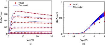
Figure 6 shows the I–V characteristics of this model and the TCAD simulation. In this model, the self-heating effect was accounted for by substituting the following equations in equation (5):


Simulated and modeled I–V characteristics of GaN HEMT: (a) I ds–V ds and (b) I ds–V gs curves.

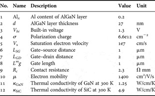
I max0 is the maximum drain current in the absence of the self-heating effect. T cIpk is the temperature coefficient of the drain current. ΔT chan, T amb, and R therm are the channel temperature, ambient temperature, and thermal resistance, respectively. In the TCAD simulation, Poisson's equation, the current continuity equation, and the heat-transfer equation were solved simultaneously for self-heating effect. The physical parameters used in this simulation are summarized in Table 1. The simulation conditions are V gs = –5 to 2 V (1 V steps) and V ds = 0–30 V (1 V steps). The models agreed well with the TCAD simulation. This result shows that this model accurately predicts the I–V characteristics from physical parameters.
Physical parameters.

III. EXPERIMENTAL VERIFICATION
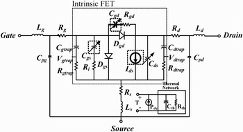
Figure 7 shows an equivalent circuit for GaN HEMT that implements the drain-current model and the capacitance model. The equivalent circuit consists of linear elements and nonlinear elements. The linear elements and the nonlinear elements represent a parasitic part and an intrinsic part in a transistor, respectively. The nonlinear elements are divided into three components which are the drain current (I ds), nonlinear capacitances (C gs, C gd, C ds), and a diode (D gs, D gd). The linear circuits are made up of parasitic inductances (L g, L d, L s), parasitic capacitances (C pg, C pd), and parasitic resistances (R g, R d, R s). This model accounts for the self-heating effect and the charge-trapping effect. A simple RC network is employed as a thermal circuit. We use a series RC network to account for the charge-trapping effect [Reference Angelov8]. The expressions for I ds, C gs, and C gd in equations (5)–(7), (10), and (11) are applied to the drain-current model, gate–source capacitance, and gate–drain capacitance.
Equivalent circuit of HEMT.

The model was verified by using a GaN HEMT including an ion implantation doping of Si under a source/drain electrode for low ohmic contacts [Reference Suita, Nanjo, Oishi, Abe and Tokuda14]. The epitaxial layers consisted of AlGaN/GaN layers grown on semi-insulating SiC substrates.
The parameter-extraction sequence of our model is simple and straightforward. For I ds parameters (I max, V knee, V p, g mpk), the initial values were extracted from the measurement of I–V characteristics. The values can also be calculated from equations (12)–(18). The other parameters were set to zero. Next, the parameters were optimized by a CAD tool.
Parameters C gs and C gd are extracted from multibias S-parameter data. Firstly, intrinsic S-parameters were obtained by de-embedding parasitic elements. Parasitic elements were extracted by means of the cold FET method [Reference Golio17]. Next, converting the S-parameters to Y-parameters, C gs and C gd were obtained [Reference Dambrine, Cappy, Helidore and Playes22]. Finally, the parameters were optimized in order to minimize the error between the measurement and model data. In the optimization, the parameters related to the carrier density were the same as the values used in parameter I ds. We can also use the values estimated from the physical parameters as the initial values for the optimization.
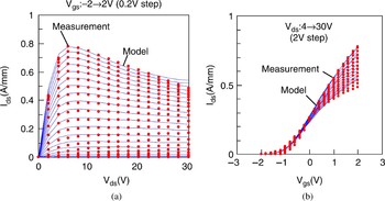
The models agreed very well with the measurement data. Figure 8 shows (a) I ds–V ds and (b) I ds–V gs curves. The measured bias conditions were over V gs from −2 to +2 V (0.2 V steps) and V ds from 0 to 30 V (2 V step). The agreement was obtained over a wide range of V ds from 0 to 30 V.
Measured and modeled I–V characteristics of GaN HEMT: (a) I ds–V ds and (b) I ds–V gs curves.

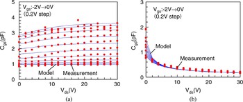
Figure 9 shows (a) C gs–V ds and (b) C gd–V ds curves. The measured bias conditions were over V gs from −2 to 0 V (0.2 V step) and V ds from 0 to 30 V (2 V steps). The model reproduced the tendency of the measurements. The model parameters C gs were equivalent to the model parameters I ds related to carrier density n.
Measured and modeled capacitance characteristics of GaN HEMT: (a) C gs–V ds and (b) C gd–V ds curves.

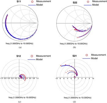
Figure 10 shows the measured and modeled multibias S-parameter. The solid line and the dotted line represent the model simulation and the measurement, respectively. Bias conditions were over V gs from −2 to 1 V (1 V steps) at V ds = 20 V. The frequency range is from 1 to 10 GHz. The agreement was obtained over a wide range of frequencies and bias values. The model accurately simulated small-signal characteristics.
Measured and modeled multibias S-parameter: (a) S11, (b) S22, (c) S12, and (d) S21 of the 0.5-mm GaN HEMT for 1–10 GHz at V gs = −2–1 V (1 V steps) and V ds = 20 V.

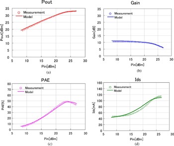
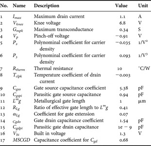
Figure 11 shows the measured and modeled LS RF characteristics of a GaN HEMT with a gate width of 0.5 mm at 9.6 GHz. The measured bias conditions were at V dsq = 30 V and I dsq = 100 mA/mm. The optimum input and output impedances at the fundamental frequency f0 and at 2f0 were determined based on a load-pull measurement. The model accurately predicted LS RF characteristics. The model parameters for nonlinear components are summarized in Table 2. This model can describe I ds, C gs, and C gd based on 17 parameters. R therm and T cIpk are the thermal resistance and temperature coefficient of the drain current, respectively. A self-heating effect was included by decreasing I ds in the high-current and high-voltage region by these parameters.
Measured (symbols) and modeled (solid lines) (a) output power, (b) gain, (c) power-added efficiency, and (d) drain current of the 0.5-mm GaN HEMT for 9.6 GHz at V dsq = 30 V and I dsq = 50 mA.

Model parameters for nonlinear components.

IV. CONCLUSION
We proposed a semi-physical nonlinear circuit model with device/physical parameters. The model equations were derived from the physical ones. A hyperbolic tangent function was used as the model equation to reproduce the electron concentration and electron velocity calculated by TCAD simulation. The I–V characteristics in the TCAD simulation could be predicted from the physical parameters used in this model.
In the model, the same physical parameters are used to model the I–V and capacitance characteristics, which are related to the electron concentration. Therefore, the model can deal directly with device/physical parameters, and it can be expressed by a very small number of model parameters (17) for nonlinear components (I ds, C gs, C gd). This model has been easily implemented in LS CAD models, by inserting the physical-based equations into equivalent circuit models.
In the verification, the LS CAD model parameters were extracted for GaN HEMT. The I–V and capacitance characteristics estimated by the model agreed well with the measurement data. Moreover, this model could be used for the accurate estimation of S-parameters and LS RF characteristics. This model is expected to be a powerful tool for improving the performance of GaN HEMTs because of its usefulness in device and circuit design. In device design, the HEMT characteristics can be estimated on the basis of the physical parameters and device structure.
ACKNOWLEDGEMENTS
The authors would like to thank Messrs. Noto and Kuwata for his support in measurement of the AlGaN/GaN HEMTs. They would also like to thank Dr. Nakayama for the review of this paper and various useful suggestions.
 Hiroshi Otsuka received the B.S. and M.S. degrees in physics from Keio University, Tokyo, in 1999 and 2001, respectively. He is with Mitsubishi Electric Corp., working in the field of research and development of microwave amplifiers for radar or telecommunication system from 2001. Mr. Otsuka is a senior member of the Institute of Electronics, Information and Communication Engineers (IEICE) of Japan.
 Toshiyuki Oishi was born in Shizuoka, Japan, in 1961. He received the B.E. and M.E. degrees in electrical engineering from Kyoto University, Kyoto, Japan, in 1984 and 1986, respectively. In 2000, he received the Ph.D. degree in ultrafine trench isolation and MOSFET for ULSI from Nagoya University, Nagoya, Japan. In 1986, he joined Central Research Laboratory, Mitsubishi Electric Corporation in Japan. From 1986, he worked on opto-electronic devices using InP related materials, trench isolation, and MOSFET in Si technologies. Since 2001, he has developed on GaN HEMT device and process technologies. From 2008, he joined Information Technology R&D Center, and started to work on modeling of GaN HEMT. He currently researches the GaN HEMT modeling designed simultaneously both device and circuit. Dr. Oishi is a member of IEEE and the Institute of Electronics, Information and Communication Engineers of Japan.
 Koji Yamanaka was born in Hyogo, Japan, in 1971. He received the B.S. degree in electric engineering in 1993 and M.S. and Ph.D. degrees in electronic engineering from University of Tokyo, Japan, in 1995 and 1998, respectively. In 1998 he joined Information Technology R&D Center, Mitsubishi Electric Corporation, where he has been engaged in the development of GaAs low-noise MMIC amplifiers and GaN high-power amplifiers. He received the Best Paper Prize in GAAS2005 for the paper entitled “S and C band Over 100 W GaN HEMT 1-chip High-Power Amplifiers with Cell Division Configuration”.
 Mattias Thorsell received his M.Sc. degree in electrical engineering from Chalmers University of Technology, Göteborg, Sweden, in 2007. He is currently working towards the Ph.D. degree at Chalmers. His main research topic is characterization and modeling of wide bandgap transistors.
 Kristoffer Andersson (S'03–M'06) received the M.Sc. and Ph.D. degrees in electrical engineering from Chalmers University of Technology, Göteborg, Sweden, in 2001 and 2006, respectively. He currently holds a position as assistant professor at Chalmers University of Technology Göteborg, Sweden. His research interests are in the area of characterization and modeling of wide bandgap transistors.
 Akira Inoue was born in Osaka, Japan, in 1961. He received the B.S. and M.S. degrees in physics from the Kyoto University, Japan, in 1984 and 1986, respectively. In 1986 he joined the LSI Laboratory, Mitsubishi Electric Corporation, where he was engaged in the development of GaAs MMIC, microwave power transistors and power amplifiers. He has been developed the first commercial inverse class-F power amplifier for mobile handsets. In 2005, he received Ph.D. degree in electrical engineering from Kobe University, Japan on the efficiency enhancement technology in microwave high-power semiconductor amplifiers. He was working on the developments of GaN and HBT power amplifiers at Information Technology R&D Center. Currently, he is a manager of the mobile phone device development section at High frequency and Optical Device Works. Dr. Inoue is a senior member of the IEEE and the Institute of Electronics, Information and Communication Engineers of Japan (IEICE).
 Yoshihito Hirano (M'94–SM'04) received the B.E. and M.E. degrees in material physics, and D.E. degrees in electronic and information engineering from Osaka University, Osaka, Japan, in 1983, 1985, and 2001, respectively. In 1985, he joined Mitsubishi Electric Corporation, Kamakura, Japan. He has been working in research on optical communication equipments, solid-state lasers, nonlinear optics, laser Radars, and microwave photonics. Dr. Hirano is a member of the Japan Society of Applied Physics, the Laser Society of Japan, the Institute of Electrical Engineers of Japan, and the Optical Society of America. He is also a senior member of IEEE Photonics Society.
 Iltcho Angelov is born in Bulgaria, received M.Sc. in electronics (with Honours) in 1969, Ph.D. in mathematics and physics from Moscow State Univversity in 1973. From 1969–1991 he was with Institute of Electronics, Bulgarian Academy of Sciences (IE BAS) Sofia as Researcher, Research Professor (1982), and Head of Department of Microwave Solid State Devices (1982). Since 1992 he is with Chalmers University, Göteborg, Sweden, as a Research Professor. His research topics are related to FET, HBT modeling, and low-noise and nonlinear circuits design.