I. INTRODUCTION
Transparent conducting electrodes (TCEs) are technologically important because of their applications in optoelectronics, flat panel displays, and solar cells. Reference Gustafsson, Cao, Treacy, Klavetter, Colaneri and Heeger1–Reference Dhar and Alford3 To maximize the performance of such devices, TCEs ought to have high transmittance in the visible spectrum and low resistance. Sn-doped indium oxide (ITO) is the most popular TCE used in optoelectronic applications because of its low resistivity and high transmittance in the visible spectrum. Reference Hosono, Ohta, Orita, Ueda and Hirano4 However, indium is a rare and expensive metal. So, there is a great demand for developing new transparent conducting oxides that can replace ITO. In this regard, a wide variety of oxides have been hitherto investigated. Reference Wan, Dattoli and Lu2,Reference Oh, Kim and Seong5–Reference Coskun and Demirel7 In addition, dielectric/metal/dielectric (D/M/D) multilayers have also been actively studied to realize both low resistivity and high transmittance in the visible spectrum.
Ag is generally used as the middle layer for D/M/D multilayers since Ag thin films (<20 nm thick) have low resistance and high transmittance in the visible spectrum. Various D/Ag/D multilayer films have been created by optimizing the compositions and the thicknesses of oxides, including SnO2, Reference Yu, Zhang, Li, Xu, Dong and Jin8 Nb2O5, Reference Dhar and Alford9 TiInZnO, Reference Kim, Kim, Lee, Park, Lee, Shin, Hwang and Heo10 MoO3, Reference Makha, Cattin, Lare, Barkat, Morsli, Addou, Khelil and Bernede11 WO3, Reference Jeon, Youn, Kim, Shin and Yang12 Al-doped ZnO, Reference Choi, Choi, Jeong, Kim and Jeon13 Al2O3, Reference Jeong and Kim14 ZrON, Reference Song, Jeon, Kim, Oh and Seong15 ZnSnO, Reference Lim, Oh, Eun, Choa, Koo, Kim and Kim16 ZnO, Reference Mohamed17 and TiO2. Reference Dhar and Alford18–Reference Jia, Zhou, Xie, You, Li and Chen20 These D/Ag/D multilayer films demonstrated good electrical and optical properties. For example, Yu et al. Reference Yu, Zhang, Li, Xu, Dong and Jin8 investigated the effects of Ag and SnO2 layer thicknesses on the electrical and optical properties of SnO2/Ag/SnO2 tri-layer films prepared on quartz glass substrates. They showed that the SnO2/Ag/SnO2 multilayer film (50 nm/5 nm/50 nm) had a maximum figure of merit (FOM) of 60 × 10−3 Ω−1 with a sheet resistance of 9.67 Ω/sq and an average transmittance of 94.8% in the visible spectrum. Mohamed Reference Mohamed17 investigated the effect of Ag and ZnO top layer thicknesses on the electrical and optical properties of ZnO/Ag/ZnO multilayer electrodes. The ZnO/Ag/ZnO multilayer (56.7 nm/Ag/56.7 nm) had a sheet resistance below 6.3 Ω/sq, when the Ag increased from 8.9 to 13.3 nm, while the transmittance varied from ∼78 to ∼93%. Calculated FOM showed that the ZnO (56.7 nm)/Ag (8.9 nm)/ZnO (39.7 nm) multilayer film was the best candidate for the application as TCEs. Furthermore, Jia et al. Reference Jia, Zhou, Xie, You, Li and Chen20 investigated the effect of Ag layer thickness on the transmittance and sheet resistance of TiO2/Ag/TiO2 multilayers and showed that the TiO2/Ag/TiO2 (10 nm/8 nm/10 nm) film had a sheet resistance of 30 Ω/sq. and a transmittance of ∼90% in the range of wave length 500–700 nm. In addition, Girtan Reference Girtan21 investigated the opto-electrical properties of ITO/Ag/ITO (20 nm/7 nm/20 nm) deposited on glass and polyethylene terephthalate (PET) substrates by successive sputtering depositions of metallic targets (In:Sn, Ag) in reactive atmosphere (for oxide) and inert atmosphere (for metallic interlayer). The multilayer films produced a resistivity of ∼3 × 10⁻⁵ Ω cm at room temperature and a transmittance of ∼90–97% at 550 nm. Subsequently, the multilayer samples on the glass and PET substrates had Haake's FOM of 21 × 10−3 and 29 × 10−3 Ω−1, respectively. In this study, we used two different oxides of ITO and TiO2 to improve the optical and electrical properties, and the mechanical flexibility of Ag-based multilayers, i.e., TiO2/Ag/ITO. This multilayer scheme was designed for use in organic light-emitting diodes (OLEDs) where 40-nm-thick ITO was used to form an ohmic contact. FOM was calculated to characterize the performance of the multilayer. The samples were subjected to bending test to investigate their mechanical flexibility.
II. EXPERIMENTAL PROCEDURE
TiO2/Ag/ITO multilayer thin films (referred to here as “TAI”) were consecutively deposited on PET substrates by a radio frequency (RF) magnetron sputtering system. Ceramic TiO2 target (99.999% purity) (purchased from LTS Inc.), ITO target (99.999% purity) (LTS Inc.), and pure Ag target (99.99% purity) (PASCO, Korea) were used at room temperature under a base pressure of ∼1 × 10⁻⁶ Torr. Before being loaded into the sputtering chamber, the PET substrates (1.5 cm2 × 1.5 cm2) were cleaned with acetone, methanol, and deionized water for 15 min per cleaning agent in an ultrasonic bath, and finally dried in a N2 stream. Prior to deposition, the TiO2, ITO, and Ag targets were presputtered for 30 min to remove contaminants. Both TiO2 and ITO were deposited at a RF power of 90 W, while Ag was deposited at 30 W. During sputtering, the PET substrate was constantly rotated at the speed of 12 rpm for TiO2 and ITO, and 23 rpm for Ag. The thickness of the Ag film was fixed at 18 nm, while the thicknesses of both the TiO2 and ITO films varied from 20 to 50 nm. For comparison purpose, 60-nm-thick ITO was also prepared (referred to here as ITO single layer). The thickness of the samples was characterized by scanning electron microscopy. The crystal structure of the multilayers was determined with x-ray diffraction (XRD, ATX-G, Rigaku, Tokyo, Japan). Hall measurements by the van der Pauw technique were carried out with a magnetic field of 0.55 T (HMS 3000, Ecopia, Gyeonggi, Korea). The four-point-probe technique was used for sheet resistance measurements. Transmittance of the multilayers was measured with a UV/visible spectrometer (UV-1800, Shimadzu, Tokyo, Japan). The mechanical flexibility of the samples was analyzed using a bending test system (ZBT-200, Z-tec, Taegu, Korea). The samples were clamped between two parallel semicircular-plates. One plate was mounted to the shaft of a motor, while the other was fixed to a supporter. The distance of the stretched mode was 45 mm and that of the bent position was 25 mm. The bending radius was approximately 15 mm and the bending frequency was 1 Hz. Finally, the resistance of the samples during the bending was measured using a multimeter.
III. RESULTS AND DISCUSSION
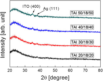
Figure 1 shows the XRD patterns obtained from the TiO2/Ag/ITO multilayer films with various oxide thicknesses. The as-deposited TiO2 layer was found to be amorphous. All of the multilayer samples have a peak at 2θ = 38.1° that corresponds to the (111) plane of Ag (JCPDS No. 87-0720). The samples excluding TiO2/Ag/ITO (20 nm/18 nm/20 nm) have a peak at 2θ = 35.0° that corresponds to the (400) plane of ITO (JCPDS No. 06-0859). It can be seen that the intensity of the (400) peaks increases with increasing ITO thickness, implying that the crystallinity becomes improved with the ITO thickness.
The XRD patterns obtained from TiO2/Ag/ITO multilayer films with various oxide thicknesses.

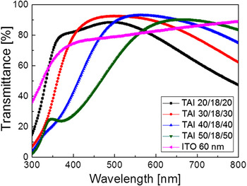
Figure 2 shows the transmittance spectra of the TiO2/Ag/ITO multilayer films as a function of the oxide thickness. Unlike the ITO single sample, the transmittance of the multilayer films reaches a global maximum around ∼480–∼660 nm and then gradually decreases with increasing wave length. The 40 nm-thick oxide multilayer sample shows the highest transmittance of 93.1% at 560 nm. The transmission window gradually shifts toward lower energies with increasing oxide layer thickness. It is noted that the 50 nm-thick sample shows a broad transmission minimum at ∼370 nm. Similar transmission minimum was found in TiO2/Ag nanoparticles/TiO2 multilayers and was ascribed to the excitation of localized surface plasmon, Reference Oh, Lee, Kim and Seong22 which corresponded to extinction peaks. Reference Temple, Mahanama, Reehal and Bagnall23 This might be also responsible for our transmission minimum although it remains to be further investigated. It is also observed that the average transmittance in the infrared region increases with increasing oxide thickness. This behavior may be attributed to plasmon-absorption-dependent reflections due to the increasing carrier concentration with decreasing TiO2 thickness. Reference Dhar and Alford9
The transmittance spectra of TiO2/Ag/ITO multilayer films as a function of the oxide thickness.

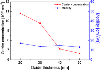
Figure 3 shows the carrier concentration and Hall mobility of the TiO2/Ag/ITO multilayer films with various oxide thicknesses. The carrier concentration gradually decreases with increasing oxide thickness; it decreases from 1.08 × 10²² to 6.66 × 1021 cm−3 as the oxide thickness increases from 20 to 50 nm, respectively. The 20 nm-thick multilayer sample shows higher mobility (17.1 cm2/V s) than other three samples with a similar mobility of 13.1–14.8 cm2/V s.
The carrier concentration and Hall mobility of the TiO2/Ag/ITO multilayer films with various oxide thicknesses.

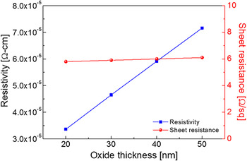
Figure 4 shows the sheet resistance and resistivity of the TiO2/Ag/ITO multilayer films with various oxide thicknesses. The sheet resistance remains almost the same; it varies from 5.8 to 6.1 Ω/sq as the oxide thickness increases. It is worth noting that the 60 nm-thick ITO single film had a sheet resistance of 144.1 Ω/sq. The resistivity also increases with increasing oxide thickness; it increases from 3.36 × 10⁻⁵ to 7.16 × 10⁻⁵ Ω cm as the oxide thickness increases from 20 to 50 nm. The resistivity is inversely proportional to the mobility and the carrier concentration. Reference Han, Mayer and Alford24 Thus, with the carrier concentration decreasing with increasing oxide thickness, this implies that the resistivity is mainly dominated by the carrier concentration, as shown in Fig. 3.
The sheet resistance and resistivity of the TiO2/Ag/ITO multilayer films with various oxide thicknesses.

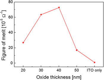
Figure 5 shows calculated FOM (φTC) of the TiO2/Ag/ITO multilayer films with various oxide thicknesses. φTC was calculated using the equation defined by Haacke, Reference Haacke25 as defined below:
 $${\varphi _{TC}} = {{T_{{\rm{av}}}^{10}} \over {{R_{\rm{s}}}}}\quad ,$$
where R s is the sheet resistance and T av is the average optical transmittance. T av can be estimated using the relation shown below:
 $${T_{{\rm{av}}}} = {{\int {V\left( \lambda \right)T\left( \lambda \right){\rm{d}}\lambda } } \over {\int {V\left( \lambda \right){\rm{d}}\lambda } }}\quad ,$$
where T(λ) is the transmittance and V(λ) is the photopic luminous efficiency function defining the standard observer for photometry. Reference Yu, Zhang, Li, Xu, Dong and Jin8,Reference Driscoll and Vaughan26 As shown in Fig. 5, the FOM reaches a maximum at 40 nm and then decreases with increasing oxide thickness. The 30 nm-thick and 40 nm-thick multilayer samples show fairly a high FOM of 63.4 and 72.8 × 10⁻³ Ω−1, respectively. As the sheet resistance changes from 5.8 to 6.1 Ω/sq. with increasing oxide thickness, the high FOMs can be ascribed to the major contribution of high transmittance.
Calculated FOM (φTC) of the TiO2/Ag/ITO multilayer films with various oxide thicknesses.

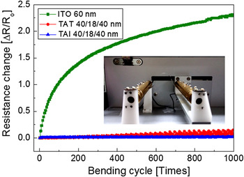
Figure 6 shows the change in resistance of the ITO single, TiO2/Ag/ITO, and TiO2/Ag/TiO2 multilayer films as a function of cycle. The change in resistance was defined as (R − R 0)/R 0, where R 0 is the initial resistance and R is the measured resistance after bend test. The value of (R − R 0)/R 0 for the ITO single film rapidly increases with increasing cycles. This is directly attributable to the generation and propagation of cracks. Conversely, the resistance of the TiO2/Ag/ITO (40 nm/18 nm/40 nm) multilayer film remains almost unchanged during the bending test. For comparison, the TiO2/Ag/TiO2 (40 nm/18 nm/40 nm) multilayer was also examined. Unlike the TiO2/Ag/ITO, the TiO2/Ag/TiO2 film remains stable up to 200 cycles, after which the resistance slightly increases during the bending test. This shows that our TiO2/Ag/ITO film has better flexibility than the TiO2/Ag/TiO2 film and ITO single films. The bending stability of the TiO2/Ag/ITO film is associated with the presence of the ductile Ag middle layer. Reference Lewis, Grego, Chalamala, Vick and Temple27 Lewis et al., Reference Lewis, Grego, Chalamala, Vick and Temple27 studying the optical, electrical, and bending properties of ITO/Ag/ITO multilayer electrodes for OLEDs, showed that the multilayer electrodes had significantly lower sheet resistance and higher average transmittance (in the range 450–650 nm) than ITO single films. The better mechanical property of the ITO/Ag/ITO multilayer electrodes was attributed to the use of ductile Ag layer with higher failure strain (4–50%). Reference Brandes, Brook and Smithells28
The change in resistance of the ITO single, TiO2/Ag/ITO, and TiO2/Ag/TiO2 multilayer films as a function of cycle. The inset shows the bending test system used in this work.

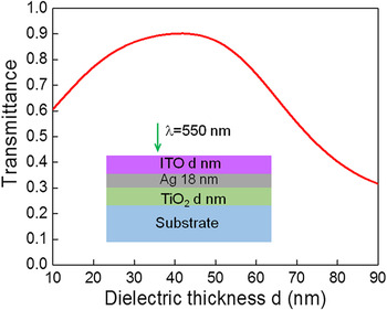
It was also shown that the TiO2/Ag/ITO multilayer films had high optical transmittance (93.1%) at a wave length of 560 nm. To rationalize the high transmittance, the relationship between transmittance and oxide thickness (d) was simulated for an Ag thickness of 18 nm using the scattering matrix method Reference Hecht29 (Fig. 7). The wave length of normally incident light was set to be 550 nm and a transparent substrate (n = 1.5) was introduced (inset in Fig. 7). The optical constants (n, k) of the used ITO, Ag, and TiO2 materials were (1.97, 0.014), (0.06, 3.19), and (2.26, 0.0), respectively. Reference Johnson and Christy30 The transmittance is sinusoidally modulated with increasing dielectric thickness and maximum at a dielectric thickness (d) of ∼40 nm, which is in a good agreement with the measured value (Fig. 2). The maximum transmittance over a range of the dielectric thicknesses (d = 30–50 nm) provides a design tolerance for actual fabrication. It is noteworthy that despite the large extinction coefficient of Ag, the maximum transmittance with the Ag thickness of 18 nm is about 90%.
Calculated transmittance of TiO2/Ag/ITO multilayer films as a function of dielectric thickness. Inset shows schematic diagram of the calculated structure.

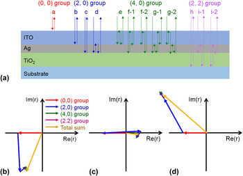
To elucidate the high transmittance of the TiO2/Ag/ITO multilayer films, we constructed phasor diagrams in which reflected partial waves are represented in the complex plane, accounting Fresnel coefficients. Reference Kats, Sharma, Lin, Genevet, Blanchard, Yang, Qazilbash, Basov, Ramanathan and Capasso31–Reference Schlich and Spolenak33 In the phasor diagrams, the four lowest orders of optical paths were taken into consideration: (m, n) = (0, 0), (2, 0), (4, 0), and (2, 2) where m(n) is the number of light's passing the ITO (TiO2) layer [Fig. 8(a)]. All the reflected partial waves in the same group undergo the same phase shift by the thicknesses of ITO and TiO2 layers and thus, the corresponding phasors belonging to the same group are rotated equally in the complex plane. Any optical path experiencing the Ag layer more than four times was not included because its magnitude becomes negligibly small. We examined three different conditions in the phase diagrams [Figs. 8(b)–8(d)]: (t, d) = (18, 10), (18, 45), and (18, 90) nm, yielding local minimum and maximum transmittance (Fig. 7). In the phasor diagrams, each group's total phasor (i.e., the total sum of partial phasors assigned to all the available optical paths) was represented in the complex plane. For the two local minimum cases [Figs. 8(b) and 8(d)], most of the total phasors are constructively added in part such that the total phasor sum is deviated from the origin in the complex plane. On the contrary, for the local maximum case [Fig. 8(c)], the magnitude of the total phasor sum is significantly reduced as the phasors are effectively canceled out each other. Therefore, these constructive and destructive interferences between reflected partial waves account for the modulation in transmittance with the dielectric thickness. These near-unity transmittances of the D/M/D multilayer films comprising a substantially thick Ag layer (t > 10 nm) can be utilized as next-generation transparent electrodes toward the development of optoelectronic devices such as organic solar cells and/or light-emitting diodes.
(a) Schematic illustration representing available optical paths belonging to the same group in TiO2/Ag/ITO multilayer films. (b–d) Phasor diagram representation for (b, d) the local minimum and (c) maximum transmittance in Fig. 7.

IV. SUMMARY AND CONCLUSIONS
We investigated the opto-electrical and bending characteristics of TiO2/Ag/ITO multilayer films on PET substrates as a function of the oxide layer thickness. The TiO2/Ag/ITO multilayer films produced the highest transmittance at 560 nm; the high transmittance was explained as a direct consequence of the antireflection effect accompanied by complex optical media. The TiO2/Ag/ITO sample exhibited much higher Haacke's FOM than the ITO. The bending test results showed that the TiO2/Ag/ITO electrode exhibited considerably improved mechanical flexibility compared to the ITO single film. The result shows that the TiO2/Ag/ITO (40 nm/18 nm/40 nm) sample can be used as an important transparent multilayer electrode in flexible photovoltaic and photonic devices.
ACKNOWLEDGMENTS
This work was supported by Korea Evaluation Institute of Industrial Technology (Grant No. 10049601). S-K.K. was supported by Basic Science Research Program through the National Research Foundation of Korea (NRF) funded by the Ministry of Science, ICT & Future Planning (NRF-2013R1A1A1059423).