


1. Introduction
The III-Nitride material system has been shown to possess great potential for applications which require devices with a wide spectral response, high breakdown voltage and high temperature and chemical stability. It is therefore highly desirable to understand and control the growth mechanisms of this material system at an atomic level so that one can manipulate the structural growth to achieve the desired properties. It is widely known that GaN epitaxial layers grown on non-native substrates contain high defect densities due to the thermal expansion coefficient and lattice mismatch between the layers. These defects include threading dislocations (TDs), stacking faults, and inversion domain boundaries. Reference Potin, Ruterana and Nouet[1], Reference Wu, Elsass, Abare, Mack, Keller, Petroff, DenBaars and Speck[2] The presence of these defects affects the optical and structural quality of the InGaN/GaN multiquantum well (MQW) structures and usually results in open V-defects at the surfaces. Reference Sun, Anwar, Chen, Yang, Khan, Shur, Byhhovski, Liliental-Weber, Kisielowski, Smith, Lin and Xiang[3], Reference Cao, Topol, Shahedipour-Sandvik, Teetsov, Sandvik, Boeuf, Ebong, Kretchmer, Stokes, Arthur, Walker and Kaloyeros[4] Due to the high intrinsic strain between the QW layers, the physical properties of the MQW structure vary strongly over distances of a few nanometers. The resultant variation in the local elastic properties strongly affects electrical and optical properties of the material and influences the growth mechanism. It has been shown that the mismatch stress causes high dislocation densities in GaN- based devices and increases the threshold current density in stimulated emission in laser structures. Reference Funato, Nakamura, Hashimoto and Ikeda[5]
The formation mechanism of the so-called V-defects in InGaN/GaN based structures is not yet well understood. The study performed by Cho et al. concluded that there are three main mechanisms for the formation of V-defects depending on the In composition of the InGaN well layer. Reference Cho, Lee and Yang[6] The origin of the V-shaped pits has also been attributed to threading dislocation defects and increased strain energy. Reference Wu, Elsass, Abare, Mack, Keller, Petroff, DenBaars and Speck[2], Reference Sun, Anwar, Chen, Yang, Khan, Shur, Byhhovski, Liliental-Weber, Kisielowski, Smith, Lin and Xiang[3], Reference Chen, Takeuchi, Amano, Akasaki, Yamada, Kaneko and Wang[7], Reference Kim, Park and Kim[8], Reference Sharma, Thomas, Tricker and Humphreyes[9], Reference Cheong, Yoon, Choi, Kim, Yu, Hong, Suh and Lee[10] Most of the previous studies on the origin of V-defects have been obtained from InGaN/GaN MQWs with In compositions of less than 20%, and only a few reports have presented results for higher In compositions. The difficulty lies in obtaining high quality MQW structures at the lower temperatures required to obtain incorporation of a high In concentration.
In this study we report on the observation of islands in the top GaN barrier surrounded by V-defects, the nature of which are studied by cross-sectional transmission electron microscopy (TEM) and wet chemical etching in combination with AFM studies. We also report on evaluation of the mechanical characteristics of these islands using ultrasonic force microscopy (UFM).
1.1 Experimental
The experimental configuration of the UFM system used in this study is similar to that reported by Dinelli et a Reference Dinelli, Catell, Ritchies, Mason, Briggs and Kolosov[11] The effect of growth temperature as well as the ambient gas (hydrogen rich versus nitrogen rich) on the GaN barrier layer and its effect on the formation of V-defects and ring defects in high In content (In~30%) InGaN/GaN MQW structures were previously reported. Reference Ting, Ramer, Flourescu, Merai, Albert, Parekh, Lee, Lu, Christini, Liu and Armour[12] Initial studies of the growth under various conditions suggested that at such high In compositions the so-called rings (previously thought of as inclusions) seem to form primarily by the 3D growth of InGaN well layer due to the high lattice strain at the initial growth stages. Here we report a detailed study of the nature of these ring defects in high In content green MQWs.
Five periods of InGaN/GaN MQWs and SQW layers were grown on a 6×2” Veeco D180 rotating disk reactor. The details of the growth have been reported elsewhere. Reference Ting, Ramer, Flourescu, Merai, Albert, Parekh, Lee, Lu, Christini, Liu and Armour[12] In order to study the origin of the ring defects a systematic study was undertaken whereby each layer was examined for its morphology evolution and its possible contribution to the V-defect and ring defect formation. Two MQW structures were deposited under similar growth conditions except for their GaN barrier layers which were deposited with 5 SLM H2 ( H2-MQW) and under H2-free conditions (growth under N2flow, only).
1.2 Results and Discussion
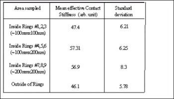
Although the surface of the H2-MQW showed a high density of pits, between the individual pits the surface was smooth and atomic steps were clearly observed. Conversely, the H2 -free MQW had a high density of whitish defects that were assumed to be inclusions in addition to a high density of pits. A close examination of these so-called inclusions under high resolution SEM revealed that they are indeed areas surrounded by pits that are closely spaced, and in some cases the pits are attached in a ring fashion forming a smooth continuous boundary (not shown here). A higher magnification image of the isolated pits forming a ring as taken by UFM is shown is Figure 1a. The details of the UFM technique has been described elsewhere. Reference Dinelli, Catell, Ritchies, Mason, Briggs and Kolosov[11], Reference Sehkwat, Kosolov, Briggs and Geer[13] The change in the stiffness of the materials using UFM technique is manifested as the UFM image contrast with softer material appearing darker than the stiffer areas. Figure 1b is the topographic AFM image of the same area taken simultaneously with the UFM image shown in Figure 1a. As noted previously, no ring defects were observed on the surface of the H2-MQW. To further investigate the structural and mechanical nature of these so-called ring defects, we studied the morphological and mechanical properties of the surfaces using UFM and AFM before and after wet chemical etching of the structures. The effective contact stiffness (CS) of the areas inside and outside of several ring defects with various dimensions were measured using UFM. To minimize experimental error we measured CS of 5 points inside of the ring defects (including center and 4 points about half way between the center and edges of the defects) using a scan size of 10 nm × 10 nm and 4 points outside and on either side of the defects using the same scan size. In order to increase accuracy UFM measurements were performed on nine inclusions of various sizes, the average CS of which is reflected in Table I. As indicated in the Table, the CS values inside and outside of the ring defects do not seem to be significantly different when taking the standard deviation value into account. It has been shown that the UFM technique can reliably differentiate between materials with above 10% difference in their Young’s modulus. Reference Dinelli, Catell, Ritchies, Mason, Briggs and Kolosov[11], Reference Kolosov, Castell, Marsh and Briggs[14] It is therefore concluded that the material enclosed in the ring defects is mainly the same as their surroundings, namely the GaN barrier material. Comparison between the CS values measured between ring defects of various dimensions (~100×100 nm2, 100×200 nm2 and 200×200 nm2) also showed values that are within the experimental error of the measurement indicating no significant difference between the mechanical properties of the islands as well. This result shows that materials within the ring defects and outside of them posses Young’s Moduli that are very close in values if not the same. To the best of our knowledge this is the first report on the use of UFM nanoscale mechanical characterization as applied to III-Nitride based system.
Values of effective contact stiffness inside, outside and between rings of various dimensions.
a) UFM image of a ring defect showing clearly the presence of holes (V-defects) surrounding an area of the top layer with different stiffness values for the holes and the surrounding material, and b) topographic AFM image of the same area taken simultaneously with the UFM image in (a) with a z-range of 20 nm.

Cho et al. reported on observation of flat regions between V-defect pits that contain larger number of stacking faults and stacking mismatch boundaries. Reference Cho, Lee and Yang[6] It has also been shown that stacking faults may result in the formation of inversion domains. Reference Cheong, Yoon, Choi, Kim, Yu, Hong, Suh and Lee[10] Additionally, the presence of inversion domains is also an indication of regions of mixed Ga and N polarity. From the UFM measurements however, it is not possible to determine the polarity change of the GaN material inside and outside of the ring defects. To do this, a hot H3PO4 acid etch technique was employed as proposed by Huang et al. in order to study the polarity of the GaN ring defects in combination with AFM characterization. Reference Huang, Reshchikov, Visconti, Yun, Baski, King and Morkoc[15] The etch rate of N-polar GaN has been reported to be on the order of 0.1−0.5 µm/min , while Ga-polar GaN material shows almost no signs of etching after long periods of etch time. A detailed account of the etching results for samples with and without ring defects have been documented. Reference Shahedipour-Sandvik, Jamil Khan, Grandusky, Wu and MacDowell[16] Figure 2a through Figure 2d show the AFM images of the MQW structure (a) before and after (b) 5 sec. (c) 10 sec. and (d) 30 sec. chemical etching. As can be seen in Figure 2 the material inside of the ring defects starts etching away in time periods as early as 5 seconds into the experiment and is completely etched away in less than 30 seconds. A closer examination of the etch rate of the ring defects inward (of the ring defect) and outward showed that the biggest cause of the island disappearance is likely not its polarity difference. Due to high etch rate of N-polar GaN it is expected that for a N-polar GaN face the material would be etched faster from top to bottom rather than from side to center. The etch rates measured by AFM showed a faster etch inward than outward away from the center. This may be due to an expansion of the separate V-defects surrounding the ring due to etching and forming a well around the ring causing a higher etch rate.
AFM images of MQW structure grown under no hydrogen a) before and after b) 5 sec., c) 10 sec., and d) 30 sec chemical etching in hot H 3 PO 4 . The AFM Z-range is a) 25nm, and b-d) 20nm.

In addition to UFM and chemical etching cross-sectional TEM was used to further investigate the nature of the inclusions. Cross-sectional TEM specimens were prepared by mechanical grinding and dimpling. Final thinning was accomplished by ion milling to perforation. Diffraction contrast images and diffraction patterns were recorded on film in a JEOL 2010F field-emission transmission electron microscope operated at 200 kV. Figure 3 shows a bright field TEM image of the feature of interest cutting through the MQW region. The pits appear facetted, with the facet making an angle of ~62° with the (0001) plane. These pits have been identified previously as V-defects. At the apex of the pit there is an extended defect which crosses the remaining MQW layers in the structure and terminates at the first QW. Although it had been suggested that the pillar in between the pits may be inverted crystallographically relative to the matrix material, convergent beam diffraction did not bear out this theory; rather no difference between the pillar and the surrounding matrix was found. Thus the extended defects are not inversion domain boundaries. To determine the nature of the extended defects, diffraction contrast images were recorded using diffraction vectors both in and out of the basal plane. Figure 4a shows a dark field image with g=

Cross-sectional bright field TEM image of the MQW sample showing cross section of a typical ring defect with dislocations attached to the apex of the V-pits clearly shown.

Dark field TEM images of the same defect shown in Figure 4 using a) and b) . The disappearance of the defect in 4b clearly indicates that the defects are pure edge dislocations.

TEM images also clearly indicate creation of edge dislocations in the QW barrier transition region. This may simply have occurred due to the attractive force between nearby threading dislocations. Typical V-defects form from threading dislocations originating at the substrate; in the ring defects observed here, however, the defects at the base of V-defect does not extend all the way to the substrate but found it energetically favorable to bend into the basal plane and join with a neighboring threading dislocation, resulting in the apparent “loop” under the hut-shaped island. Although the basal plane is not a preferred plane for dislocation formation in nitrides, it seems clear that the new configuration had a significant reduction in line length, and thus was energetically favored. The arrangement of the V-defects on the surface forming rings seems to duplicate the cellular shape of InGaN QWs observed in AFM studies (not shown here). Reference Ting, Ramer, Flourescu, Merai, Albert, Parekh, Lee, Lu, Christini, Liu and Armour[12] Use of higher growth temperature (increasing surface mobility) or incorporation of hydrogen (creating a chemical path way to etch away weaker bonds) is shown to completely eliminate the ring defects. At such high In composition (>30%) growth at relatively lower temperature (700°C) can result in poor surface migration of Ga on the basal surface deteriorating the 2D growth and stabilizing formation of V-pits.
1.3 Conclusion
In summary, we have reported on the use of UFM technique for nanoscale mechanical characterization of GaN. Observation of ring like defects which appear to be resulting from high In content of the well layer grown at lower (less than 800 °C) temperature and/or under no hydrogen flow was also reported. Nano-mechanical properties of the ring defects as measured by UFM showed no meaningful variation in the contact stiffness of the areas inside and outside of the defects supporting the material similarity amongst the ring defects and the surrounding regions. Through cross sectional TEM analysis as well as wet chemical etching the possibility of existence of inversion domains in regions within the ring defects was ruled out.
Acknowledgments
The authors would like to thank M. McDowell for help with chemical etching of the structures. This work was partially funded by General Electric Global Research Center located in Niskayuna, NY and by Veeco Corp. located in Somerset, NJ.



