I. INTRODUCTION
Due to low weight, ruggedness, low costs, large area, and ease of integration, flexible electronics have become a major research trend in recent years. Reference Rim, Bae, Chen, De Marco and Yang1–Reference Heremans, Tripathi, de Jamblinne de Meux, Smits, Hou, Pourtois and Gelinck3 Mechanical stability is a precondition for flexible electronics to function well. The thin metal film as an electrical interconnect between electronic units is one of the weakest components in the system against mechanical deformation. Reference Rim, Bae, Chen, De Marco and Yang1,Reference Heremans, Tripathi, de Jamblinne de Meux, Smits, Hou, Pourtois and Gelinck3 Thus, it is necessary to understand the fundamental deformation mechanisms of metal films bonded to flexible substrates so as to build high-performance flexible electronics.
The mechanical behavior of metal films bonded to the flexible substrates is substantially different from that of their bulk counterparts. For freestanding films, the fracture strain is quite low (about 1–2%) and they rupture by forming a single necking. Reference Huang and Spaepen4–Reference Pashley6 By contrast, a flexible substrate can suppress strain localization and retard necking in the film, and it finally causes multiple neckings before rupture in the film. Reference Lu, Wang, Suo and Vlassak7–Reference Li, Huang, Suo, Lacour and Wagner10 The rupture strains (stretchability) of thin metal films (including Cu, Ag and Au films) on flexible substrates can be up to 10%. Reference Alaca, Saif and Sehitoglu5,Reference Hommel and Kraft11–Reference Niu15 For metal films well bonded to the substrates, the failure strain can be dramatically enhanced beyond 50%. Reference Lu, Wang, Suo and Vlassak7–Reference Sim, Won, Jin, Park, Lee and Vlassak9,Reference Arafat, Dutta and Panat16 The film thickness studied is mostly above the nanometer scale.
Recently, the ongoing miniaturization in thin film technology has led to a drastic reduction in the dimensions of the component elements and an urgent need to understand the basic deformation behaviors of small-scale materials. Due to confinement effects, metal films on flexible substrates exhibit prominent size-dependent deformation mechanisms. It has been found that thinner films with a thickness below 200 nm failed by intergranular fracture at elongations by only a few percent, while thicker films were ruptured by ductile transgranular fracture and local debonding from the substrate. Reference Lu, Suo and Vlassak8 When the film thickness decreases below 100 nm, plasticity decreases dramatically due to dimensional constraints on dislocation activity. Reference Sim, Won and Lee17 A transition of the dominating deformation mechanism from perfect to partial dislocations has been found in films with the thickness below 80 nm on substrates. Reference Gruber, Solenthaler, Arzt and Spolenak18–Reference Luo, Zhu and Zhang20 Meanwhile, grain growth has been frequently observed in the ultrathin films under tensile loading. Reference Lu, Wang, Suo and Vlassak21 The grown grains were found to be the preferential sites for strain localization, resulting in an unstable deformation process. Reference Lu, Wang, Suo and Vlassak21,Reference Höppel, Zhou, Mughrabi and Valiev22 Till now, there is still lack of a deep understanding of the fracture behaviors and deformation mechanisms in the mechanically unstable thin films on the flexible substrate with a film thickness ranging from the micron scale to the nanometer scale, especially in terms of microscopic aspect.
In the present study, a systematic investigation on grain growth and mechanical behaviors was performed on nanocrystalline (NC) Au films with a thickness ranging from 20 to 930 nm. Through the quantitative evaluation of microstructure evolution, the scaling effect on stretchability of the NC Au films bonded to polyimide substrates under tensile loading was elucidated.
II. EXPERIMENTAL
Au films (target purity: 99.99%) with a thickness (h) of 930, 170, 90, 40, and 20 nm were deposited onto 125 μm-thick polyimide (Dupont™ Kapton®, Wilmington, Delaware) substrates using DC magnetron sputtering under ultra-high vacuum (10−7 torr) conditions. Before deposition, the substrate was cleaned by sputtering Ar ions for about 5 min to remove the surface contamination and to improve the bond between the substrate and the film. The as-deposited film has a well-equiaxed structure and the average in-plane grain size, ranging from 19 nm in the 20 nm-thick film, 14 nm in the 40 nm-thick film, 36 nm in the 90 nm-thick film, 42 nm in the 170 nm-thick film, to 52 nm in the 930 nm-thick film, increases with increasing the film thickness. Reference Luo and Zhang23
X-ray diffraction θ–2θ scans were performed on a Rigaku X-ray diffractometer D/MAX–2500/PC (Rigaku Corp., Tokyo, Japan) equipped with Cu Kα radiation (56 kV, 182 mA), which show that all the films have the 〈111〉 out of plane texture. Surface morphologies were characterized by a field-emission scanning electron microscopy (SEM; Zeiss Supra 35, Carl Zeiss Microscopy, Cambridge, England) under an accelerating voltage of 20 kV. The as-deposited and tensiled samples were characterized by field-emission transmission electron microscopies (TEMs; FEI Tecnai F20, FEI, Hillsboro, Oregon). The high-resolution TEM (HRTEM) observations were conducted on FEI Tecnai F20 at 200 KV with a point resolution of ∼0.21 nm. The dislocation observation was performed using the two-beam condition. Samples for HRTEM and TEM observations were first mechanically ground to ∼30 μm in thickness and then were further thinned from the substrate side by ion milling method on a precision ion polishing system (Gatan 691, Gatan, Inc., Pleasanton, California) at −100 °C.
Tensile testing of the film samples with a gauge section of 10 mm in length and 2 mm in width was performed on a microforce testing system (MMT-101NV-10, SHIMADZU, Kyoto, Japan). All tests were performed at room temperature at a constant strain rate of 6.3 × 10⁻⁴ s−1. A real-time electrical resistance (R) of the film was measured during tensile testing using a digital multimeter (Agilent 34410A, Agilent Technologies, Santa Clara, California) with a resolution of 10−3 Ω to determine the failure strain (εf).
III. RESULTS AND DISCUSSION
A. Determination of failure strains
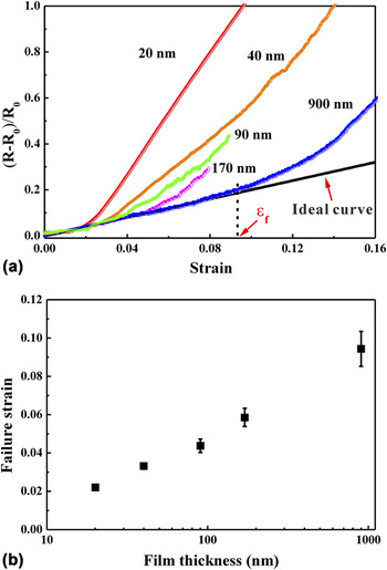
Figure 1(a) presents relations between the relative resistance ΔR/R 0 = (R − R 0)/R 0 and the applied strain (ε) for the Au films with a thickness ranging from 930 to 20 nm, showing that ΔR/R 0 gradually increases with increasing ε. At the beginning of the deformation, the films elastically deform with the conserved volume, and the ideal resistance curve is described by the following equation, Reference Lu, Wang, Suo and Vlassak7
 $${{\Delta R} \mathord{\left/ {\vphantom {{\Delta R} {{R_0}}}} \right. \kern-\nulldelimiterspace} {{R_0}}} = {\varepsilon ^2} + 2\varepsilon \quad .$$
(a) Relative resistance increase, (R − R 0)/R 0, versus the applied strain in the Au films with different film thicknesses under tensile loading. The straight line is an ideal resistance curve plotted by Eq. (1). (b) Relation between critical failure strains of the Au films and film thickness.

Deviation from the ideal resistance curve has been reported to be related to the nucleation and propagation of cracks in the film. Reference Lu, Wang, Suo and Vlassak7,Reference Lu, Suo and Vlassak8,Reference Niu15,Reference Sim, Won and Lee17,Reference Luo, Zhu and Zhang20,Reference Kim, Shin, Lee, Yang, Haas, Gruber, Choi, Kraft and Joo24 The critical failure strain (εf) is determined to be a strain at which an increase of ΔR/R 0 deviates from the ideal value by more than 5% [see Fig. 1(a)], where the microcracks start to propagate. Reference Lu, Suo and Vlassak8,Reference Sim, Won and Lee17,Reference Luo, Zhu and Zhang20 The measured failure strains are shown in Fig. 1(b), indicating that the failure strain decreases with decreasing the film thickness. The 930 nm-thick film has the largest failure strain of 9.4% among the six groups of the studied samples. When decreasing the film thickness from 170 to 20 nm, the failure strain decreases from 5.9 to 2.2%.
B. Damage morphology
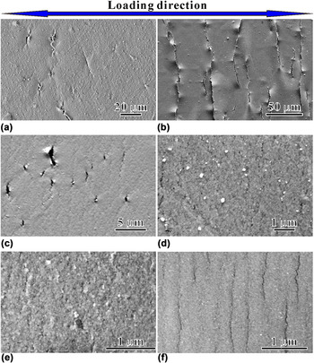
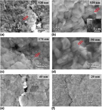
Figure 2 shows surface damage morphologies in the Au films with different film thicknesses, indicating that the main failure modes were multiple microcrack initiations, crack propagations and connections with each other, and finally delamination of the Au film from the polyimide substrate. Close observations in Figs. 3(a) and 3(b) show that intense slip traces locally occurred in the grown grains in the 930 nm-thick film. The further TEM observation [see an inset in Fig. 3(b)] proves that abnormal grain growth happened which provided enough space for the full dislocation motion. When decreasing the film thickness down to 170 and 90 nm, we could also observe some slip traces of dislocations, as shown in Figs. 3(c) and 3(d). Generally, the cracks seem to initiate in regions plastically deformed, where local thinning appeared when h ≥ 90 nm. The cross-sectional observations show that the local thinning was accompanied by simultaneous debonding of the metal film from the substrate, consequently the film became freestanding to form necking. Reference Lu, Wang, Suo and Vlassak21 On further decreasing the film thickness to 40 and 20 nm, no slip lines could be observed, as shown in Figs. 3(e) and 3(f). The main damage behaviors were intergranular cracks. Obviously, the damage behaviors of the films exhibited a strong length-scale dependence with decreasing the film thickness.
SEM observations of the surface damage morphologies in the Au films with the film thickness of (a) and (b) 930 nm, (c) 170 nm, (d) 90 nm, (e) 40 nm, and (f) 20 nm, respectively. The loading direction is the horizontal direction.

Close observations of damage morphologies in the Au films with the film thickness of (a) 930 nm, (b) abnormally grown grains in 930 nm-thick film, (c) 170 nm, (d) 90 nm, (e) 40 nm, and (f) 20 nm-thick films.

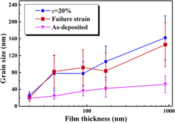
Even though the film thickness is up to micron scale, the full dislocation activities are limited in the initial nanometer-sized grains. However, the fact that slip traces induced by dislocation gliding formed even in the 90 nm-thick film indicates that grain growth might happen during the tensile loading. Figure 4 shows the statistical result of the grain size of the Au film deformed to the failure strain and the strain of 20% which allows formation of more cracks. It indicates that grain growth indeed happened in the films except for the 20 nm-thick film. The average grain size in the 930 nm-thick film can be up to submicron sizes, and some grains can abnormally grow to the micron scale; in the 170, 90, and 40 nm-thick films, the average grain size is around 100 nm. The regions for the grain size measurement were the uncracking regions in the deformed Au films because of the difficulty in preparing TEM samples around the tensile cracks. The average grain size in the uncracking regions under failure strains is similar to that of samples with higher crack densities under enhanced applied strains, indicating that cracking has a negligible effect on the average grain size in the uncracked regions. The grown grains would provide the needed space for the observed dislocation motion, which will be discussed in the following.
Average grain size of the Au films with different film thicknesses subjected to different tensile strains. The grain size of the as-deposited films is for a comparison.

C. Dislocation mechanisms-some TEM observations
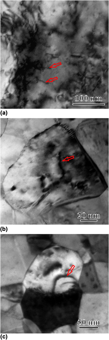
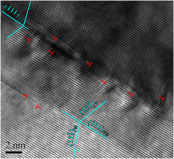
When the film thickness decreases to around 1 μm, the lattice defects may begin to “feel” the presence of the surface and interface; as a result, the deformation mechanisms are subject to size effects. Reference Arzt25,Reference Zhang, Wang and Sih26 In the 930 nm-thick film, we observed plenty of dislocations and dislocation pileups in the submicron-size grain, as indicated by the arrows in Fig. 5(a), which is consistent with the observation of extensive slip traces in Figs. 3(a) and 3(b). These large grains actually became the preferential sites for strain localization and thus indeed sustained a certain plastic strain. It was reported that grain growth could significantly increase the ultimate tensile strain, Reference Gianola, Van Petegem, Legros, Brandstetter, Van Swygenhoven and Hemker27,Reference Fan, Fu, Wang, Ren, Choo, Liaw, Wang and Browning28 thus the stretchability of the 930 nm-thick film is the best due to the most active full dislocation behavior. When the film thickness decreases to 170 nm, the less slip traces indicate that the dislocation motion becomes weak. However, a Frank–Read-type dislocation source was observed inside the grain with a diameter of about 110 nm, as shown in Fig. 5(b). Such a Frank-Read-type source was also observed previously, and the minimum size of this source was estimated to be ∼200 ± 20 nm. Reference Dehm, Legros and Heiland29 Thus, the observed dislocation source may lay on an inclined {111} plane in the 170 nm-thick film. Besides, even in the nanotwinned grains in the 170 nm-thick film, we could also observe plenty of full dislocations (see Fig. 6), indicating that such film thicknesses can provide space for the dislocation motion in the slip planes inclined to the film surface. When the film thickness and/or the grain size decreases to 100 nm, it was found that the grain boundary (GB) would take up a large volume fraction; the dislocation source (Frank–Read-type source) was hard to be operated. Reference Meyers, Mishra and Benson30 However, individual dislocations could also be observed in a grain with a size of about 140 nm, and the GBs were found to be an effective source for dislocation nucleation in the 90 nm-thick Au film. It was suggested that GB ledges would be the active source for dislocation emissions. Reference Murr and Wang31,Reference Price and Hirth32 Generally, the full dislocation behavior became the dominate deformation mechanism when h ≥ 90 nm. Our experimental observations indicate that full dislocation behaviors were contributed to the local thinning in the thicker ductile films, as shown in Fig. 3.
Dislocation structures in the (a) 930 nm, (b) 170 nm, and (c) 90 nm-thick Au films after tensile testing. Positions of the dislocation lines are indicated by the arrows.

HRTEM image of dislocations in the nanotwins of the 170 nm-thick Au film after tensile testing. The twin relationship is indicated by the straight lines. “⊥” indicates a dislocation.

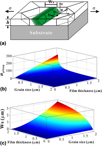
Based on the above observations, we can further understand the size effect by the dislocation pileup theory in the film on a substrate, Reference Zhang, Volkert, Schwaiger, Wellner, Arzt and Kraft33 as shown in Fig. 7(a). In a film with the film thickness (h) and grain size (d), dislocations with a Burgers vector of b glide on the slip plane under the applied stress σ, causing the film yielding and thus the number of pileup dislocations (n pileup) can be described by Reference Zhang, Volkert, Schwaiger, Wellner, Arzt and Kraft33,Reference Thompson34
 $${n_{{\rm{pileup}}}} = {{\pi \left( {1 - \nu } \right){\tau _{\rm{y}}} \cdot h} \over {G\bi {b}\sin \varphi }}\quad ,$$
where τy is the yield stress, ν is the Poisson’s ratio, G is the shear modulus, λ is the angle between b and the normal direction of the film surface, and φ is the angle of the slip plane normal with the film surface normal.
(a) Schematic of the geometry for dislocation gliding-induced slip bands in a thin film constrained by a substrate. Reference Zhang, Volkert, Schwaiger, Wellner, Arzt and Kraft33 (b) Calculation of the number of pileup dislocations predicted by Eqs. (2) and (3) as a function of film thickness and grain size. (c) Calculation of width of the surface slip band (W s) predicted by Eq. (4) as a function of film thickness and grain size for a given plastic strain of 1% and n = 8.

According to the threading dislocation theory in the film on a substrate, the yield stress is given by Reference Zhang, Volkert, Schwaiger, Wellner, Arzt and Kraft33,Reference Thompson34
 $${\tau _{\rm{y}}} = {{G\bi {b}} \over {4\pi \left( {1 - \nu } \right)}}\ln \left( {{D \over \bi{b}}} \right)\left( {{2 \over d} + {{\sin \varphi } \over h}} \right)\quad .$$
For Au, Reference Oh, Legros, Kiener, Gruber and Dehm19 G = 27 GPa, a = 0.408 nm, ν = 0.42, and φ = 45°. Based on Eqs. (2) and (3), we can calculate n pileup in films with different h and d, as shown in Fig. 7(b). We can see from Fig. 7(b) that n pileup decreases with decrease h and/or d. This can explain why thinner films have poor stretchability.
Besides, if the film has enough mobile dislocations, the glide of n dislocations on the slip plane to the film surface would cause the formation of a step with a height of n· b ·cos λ. A slip band consists of N slip slip planes [see Fig. 7(a)]. Thus, we can calculate the width of the slip bands (W s) under the total applied plasticity strain εpl by Reference Zhang, Volkert, Schwaiger, Wellner, Arzt and Kraft33
 $${W_{\rm{s}}} = \left( {{{{\varepsilon _{{\rm{pl}}}}d} \over {n\bi {b}\sin \lambda }} - 1} \right) \cdot \,{1 \over {2\ln \left( {{d \over \bi {b}}} \right) \cdot \left( {{2 \over d} + {{\sin \varphi } \over h}} \right)}}\quad .$$
From Eq. (4), we calculate W s for the tensiled films with a different h and d, as shown in Fig. 7(c). We can see from Fig. 7(c) that W s decreases with decreasing h and/or d. This may explain the occurrence of the extensive slip traces in the 930 nm-thick film after tensile deformation. When decreasing the film thickness (the grain size also decreases), both the number of mobile dislocations and the width of the slip band decrease, as shown in Figs. 7(b) and 7(c). Consequently, the slip traces at the grain surface become fewer and fewer and get harder to be detected under the SEM, as shown in Figs. 3(c) and 3(d).
When the film thickness further decreases to several tens of nanometers, the critical stress for the activation of full dislocations (τN) becomes higher than that for partial dislocations (τp), and the films exhibit a large tendency toward the formation of stacking faults and twins. Reference Gruber, Solenthaler, Arzt and Spolenak18–Reference Luo, Zhu and Zhang20 We can calculate τN and τp by, Reference Zhu, Liao, Srinivasan, Zhao, Baskes, Zhou and Lavernia35,Reference Zhu, Liao, Srinivasan and Lavernia36
 $${\tau _{\rm{N}}} = {{Ga} \over {2\sqrt 2 \pi \left( {1 - v} \right)d\cos \alpha }}\ln {{\sqrt 2 d} \over a}\quad .$$
 $${\tau _{\rm{P}}} = {1 \over {\cos \left( {\alpha - 30^\circ } \right)}}\left[ {{{\sqrt 6 \gamma } \over a} + {{Ga\left( {1 - v} \right)} \over {8\sqrt 6 \pi \left( {1 - v} \right)d}}\ln {{\sqrt 2 d} \over a}} \right]\quad ,$$
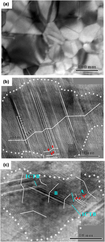
where γ is the stacking fault energy and γ = 40 mJ/m2, a is the lattice parameter and a = 0.408 nm, d is the grain size or the film thickness, and 90° − α is the angle between the shear stress and the Burgers vector, and α = 25°. Reference Oh, Legros, Kiener, Gruber and Dehm19 When the grain size or film thickness is below a critical size (d B), τP < τN, partial dislocation behavior becomes a governing mechanism. According to Eqs. (5) and (6), d B is ∼40 nm here. Generally, the smaller length scale between the grain size and the film thickness would be the key factor for the dislocation motion constraint. Grain coarsening happened after the tensile testing and the grain size got larger than the film thickness when h < 90 nm, as shown in Fig. 4, thus the full dislocation behavior was constrained by the film thickness and partial dislocation behavior prevailed in the films with thicknesses of 40 and 20 nm. Reference Luo, Zhu and Zhang20 This can be evidenced by the appearance of plenty of multiple nanotwins in the 40 and 20 nm-thick films, as shown in Fig. 8. The twins may have twin boundaries parallel to each other [Fig. 8(b)] and/or intersecting with each other at certain angles [Fig. 8(c)]. The discontinuity of the twin boundaries indicated by arrows in Figs. 8(b) and 8(c) indicates the presence of Shockley partials at the twin boundary and that those partial dislocations were usually emitted from GBs. Reference Zhu, Liao and Wu37 Consequently, the GBs become the preferential sites of cracking initiation, and the films exhibited the brittle fracture behavior.
(a) A TEM image of the twinned grains in the 40 nm-thick film after tensile testing. (b) and (c) HRTEM images of the multi-twins in the 20 nm-thick Au film after tensile testing. The twin relationship is indicated by the straight lines. The dashed lines indicate the incoherent twin boundaries. The stars indicate the GBs. The arrows indicate positions of the twin boundaries.

The present finding on the deformation-mechanism dependent stretchability of the NC Au films on flexible substrates may be of importance for the design of flexible electronics with high reliability, such as metal films with grain sizes and/or film thicknesses that are too small to allow abundant dislocation motions which would have poor stretchability, while the annealing treatment to obtain stable and uniform large grains would be helpful for deformation delocalization and enhance the stretchability and even fatigue reliability. Reference Zhang, Xiao, Luo, Zhu and Zhang38
IV. CONCLUSIONS
We have carried out uniaxial tensile experiments on the NC Au films bonded to the polyimide substrates with a thickness ranging from 930 to 20 nm. The following conclusions can be drawn:
-
(1) The 930 nm-thick film had the maximum failure strain (9.4%), and the failure strain decreases with decreasing the film thickness. Grain growth happened in the films subjected to tensile loading except for the 20 nm-thick film.
-
(2) Experimental observations and the theoretical analysis show that with decreasing the film thickness (the grain size also decreases) both the number of mobile dislocations and the width of the slip band decrease. When h ≥ 90, local thinning caused by intense plastic deformation occurred in the grown grains. Full dislocation behavior was the dominated deformation mechanism in the films: dislocation pileup in the h = 930 nm film, the Frank–Read-type source in the h = 170 nm film, and the GB dislocation source in the h = 90 nm film. Films showed the ductile fracture behavior.
-
(3) When h ≤ 40 nm, the films failed at very low strains as a result of intergranular fracture. The films exhibited a large tendency of the partial dislocation behavior and the brittle fracture behavior.
ACKNOWLEDGMENTS
This work was supported by the National Natural Science Foundation of China (NSFC, Grant Nos. 51601198 and 51571199) and partially supported by the NSFC (Grant No. 51371180).