Introduction
With the rapid development of technologies involved in data storage devices, the innovative memory with simple fabricated process, high usability and environmentally-friendly characteristics have become essential demands [Reference Strukov and Kohlstedt1, Reference Qian, Nguyen, Chen and Lee2]. Resistive random access memory (RRAM), which is expected to replace the entrenched incumbent technologies, has been investigated in detail using a variety of materials in efforts to improve the capacity, density, and write/erase speed of digital memories [Reference Chang, Chang, Tsai, Chu and Sze3]. Among numerous kinds of switching layer materials, RRAMs based on polymer thin films are preferred because of their polymeric networks, which are very versatile when applied in flexible devices [Reference Hosseini and Lee4, Reference Lee, Bae, Seong, Il Lee, Park, Choi, Im, Kim and Choi5]. Chitosan, a biopolymer, is derived from chitin, which can be extracted from cell waste of shrimps, lobsters, krill, and crab [Reference Silva, Braga, Fook, Raposo, Carvalho and Canedo6]. These sources are available in nature and inexpensive and will thus be an ideal direction for industrial-scale production. The low conductivity and mechanical strength of chitosan make it particularly suitable for the insulator layer in an RRAM structure. In recent years, a few reports of chitosan film–based memory devices have been made by Hosseini et al. [Reference Hosseini and Lee4, Reference Raeis-Hosseini and Lee7, Reference Raeis-Hosseini and Lee8, Reference Raeis Hosseini and Lee9], in which chitosan was doped with Ag or mixed with another polymer to form a composite. Some other authors reported the use of a chitosan electrolyte as the gate dielectric in transistors [Reference Zhu, Chao, Xiao, Liu and Wan10, Reference Morgado, Pereira, Bragança, Ferreira and Fernandes11]. Employing nanoparticle incorporation and acid doping, Peng et al. also optimized the properties of chitosan for double-layer transistors [Reference Shao, Wan, Yang, Du and Feng12]. These reports exhibit the high potential of chitosan materials in electronic devices. Herein, we fabricated the chitosan film as a switching layer–based RRAM device and investigated the influence of top electrodes on the resistive switching (RS) effect. Furthermore, the electrical conduction and RS mechanisms of devices were analyzed thoroughly. This study provides additional understanding of the RS mechanism for biodegradable memory devices used in information storage systems.
Results and discussion
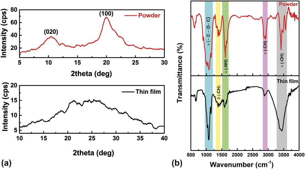
The crystalline structure of the chitosan thin film was determined by X-ray diffraction (XRD). The XRD patterns obtained for the chitosan powder and chitosan thin film are shown in Fig. 1(a). We can see two prominent peaks for chitosan powder: the sharp higher peak at around 2θ = 20.02° can be attributed to the (100) plane, while the lower one at 2θ = 10.53° can be assigned to the (020) plane [Reference Farshi Azhar, Olad and Salehi13]. Because of the presence of free NH2 groups that cause intermolecular hydrogen bonding and periodicity within the molecular structure, the chitosan powder was partially crystalized [Reference Ray, Pal, Anis and Banthia14]. We know that the dissolution of chitosan powder in acetic acid solution distributed it evenly in solution, making crystallization difficult, and therefore, the chitosan thin film was almost amorphous. Therefore, the XRD pattern of the chitosan thin film exhibited only one broad peak in the range 15–35° with a lower intensity than that of the powder pattern, which suggested that the chitosan powder did not dissolve completely in the acetic acid solution.
(a) XRD pattern and (b) FTIR spectra of chitosan powder and thin film.
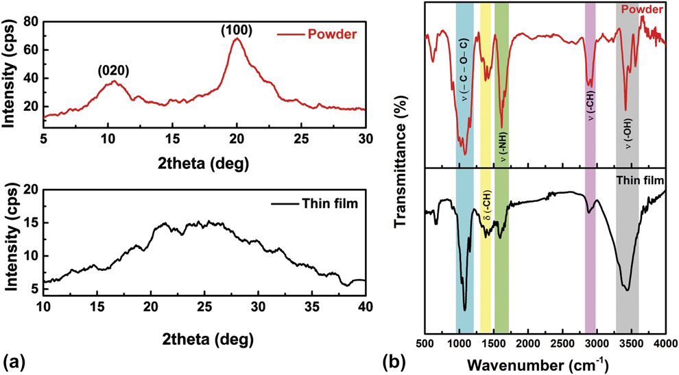
To confirm the chemical structure of the chitosan powder and thin film, Fourier transform infrared spectroscopy (FTIR) spectra were recorded in the range 400–4000 cm−1, as shown in Fig. 1(b). In general, both curves of chitosan powder and thin film get the specified peaks in the same wavenumbers that are listed as follow. A relatively high and broad band can be observed at around 3429 cm−1, corresponding to O–H stretching vibrations and overlaps from N–H vibrations [Reference Kumirska, Czerwicka, Kaczyński, Bychowska, Brzozowski, Thöming and Stepnowski15]. The C–H aliphatic stretching vibration appeared at 2885 cm−1 band while the absorption peak at 1640 cm−1 corresponds to an amide II band and the stretching vibration of the C–O of acetyl groups in the retained chitin [Reference Kumirska, Czerwicka, Kaczyński, Bychowska, Brzozowski, Thöming and Stepnowski15, Reference Rumengan, Suryanto, Modaso, Wullur, Tallei and Limbong16]. Weak vibrations owing to asymmetrical C–H bending occurred at 1380 cm−1, while the strongest vibration of C–O stretching and C–O–C bridge stretching were indicated by the sharp band at 1031 cm−1 and 1155 cm−1, respectively [Reference Dimzon and Knepper17]. The intensity of N–H stretching was seen that being equivalent to the C–H bending in chitosan thin film, whereas the intensity of those according vibrations is different in powder sample. This can be explained from the interaction between amine group and acid acetic solvent [Reference Adlim and Bakar18]. According to the appearance of the vibrational peaks, the thin film was confirmed to be composed of chitosan.
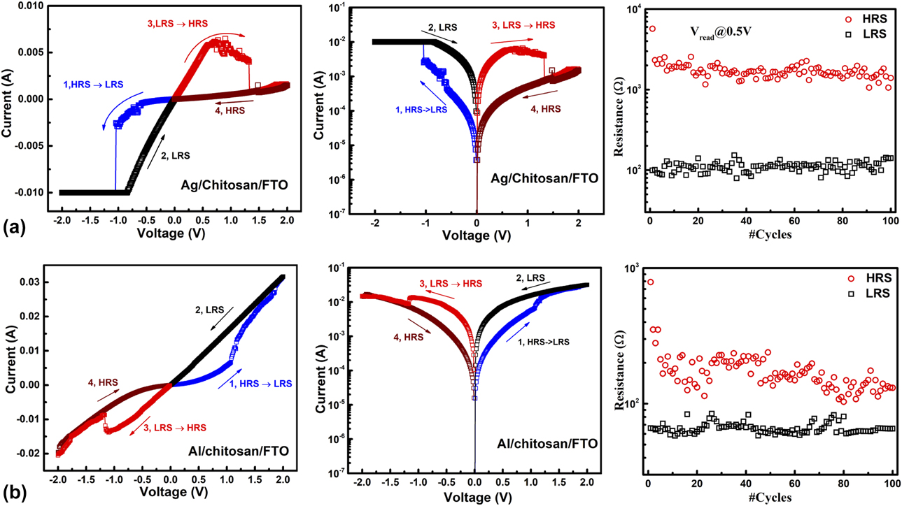
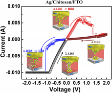
The I–V characteristics of the resistive memory devices were investigated by applying a voltage to a configuration in which the Ag or Al top electrode was grounded and the fluorine-doped tin oxide (FTO) bottom electrode was biased. To evaluate the RS behavior of the Ag/chitosan/FTO structure, we applied a voltage in two different sequences: 0 V → 2 V (or 0 V → −2 V) and 0 V → −2 V → 0 V → 2 V → 0 V. The results indicated only bipolar RS characteristics for the memory devices. The I–V curves showed bipolar RS for the Ag/chitosan/FTO structure in Fig. 2(a). At the first voltage sweep from 0 V to −2 V, the set process was formed at V set ≈ −1 V when the current abruptly increased to 102 A. The pristine high-resistance state (HRS) transformed to a low-resistance state (LRS), which was maintained during the reverse sequence from −2 to 0 V until the opposite polarity voltage of 0–2 V was introduced. The device was then switched from the LRS to the HRS at V reset ≈ 1.3 V as the current dropped to ∼104 A, which was retained during the voltage sweep back to 0 V again. The I–V characteristics suggested reversible RS behavior of the Ag/chitosan/FTO structure. The transition from the HRS to the LRS occurred when applying a negative bias to the bottom FTO electrode and the reverse switching attained when the bottom electrode was positive biased. The results of the endurance tests conducted over 100 repeated cycles, as seen in Fig. 2(a), suggested reliable and stable RS behavior of the device. Both V set ≈ −1 V and V reset ≈ 1.3 V are lower than 2 V and the On/Off ratio was larger than ten times, which is able to be considered for electronic memory device applications.
The I–V characteristics of (a) Ag/chitosan/FTO and (b) Al/chitosan/FTO devices.
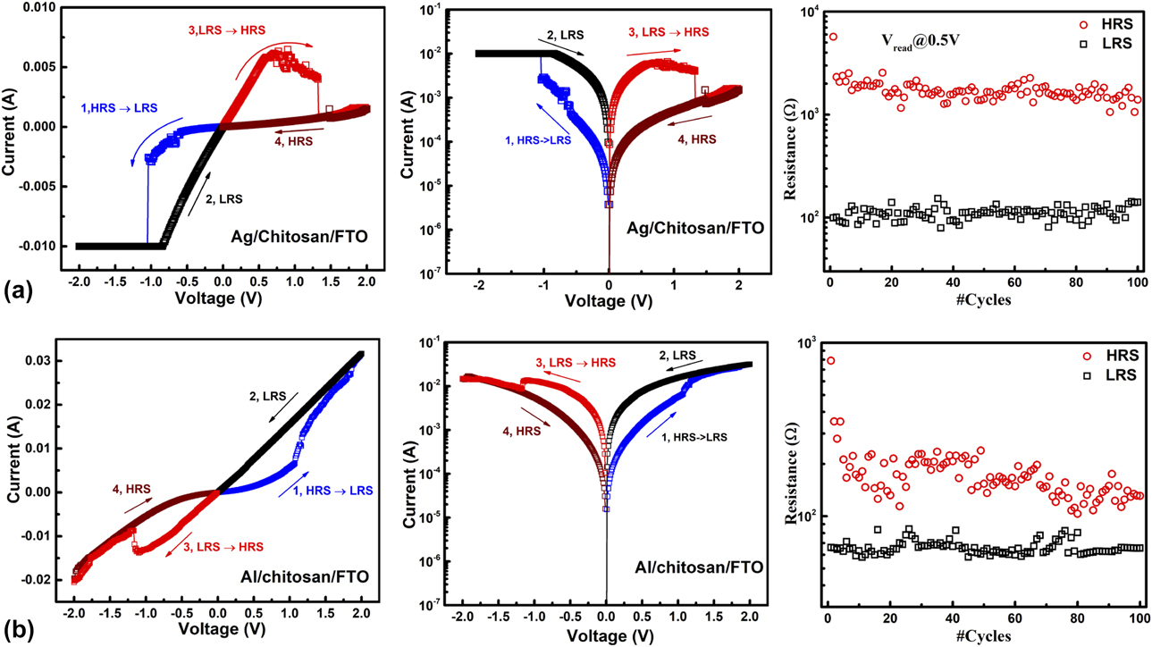
To examine the dependence of the I–V characteristics on various electrodes, we replaced the top Ag electrode with Al (the same work function ϕ ≈ 4.2 eV but less oxidation). The I–V characteristics of the Al/chitosan/FTO structure are shown in Fig. 2(b): the set and reset effects appeared in the reverse direction of that of the Ag/chitosan/FTO structure. The voltage was swept in the sequence 0 V → 2 V → 0 V → −2 V → 0 V with the initial state in the HRS. In the first voltage sweep from 0 to 2 V, the current of the device increased steadily up to 1 V, from which the current increased more rapidly and switched from the HRS to the LRS during the sweep from 1 to 2 V. After it was established, the LRS was retained until an opposite voltage sweep from 0 to −2 V was applied. At −1.2 V, the current decreased slowly and switched from the LRS to the HRS, which was maintained throughout the sweep from −2 to 0 V. The endurance test of the Al/chitosan/FTO structure was executed for 100 cycles, and the results shown in Fig. 2(b) demonstrate that the On/Off ratio for the Al/chitosan/FTO structure was lower and less stable than that of the Ag/chitosan/FTO one. In both structures, a compliance current of 0.5 A was set up to avoid the permanent breakdown through the 300 nm thickness chitosan film during repeated sweeps. The I–V characteristics of both structures implied bipolar RS behavior. However, using different metals for the top electrodes changed the direction of the switching process [Reference Raeis-Hosseini and Lee8] and the reliability of device. Compared with the Al/chitosan/FTO configuration, which showed gradual switching, the configuration with the Ag electrode exhibited more abrupt switching behavior. That means the Ag/chitosan/FTO device will operate more apparently between write and erase process than the Al alternative.
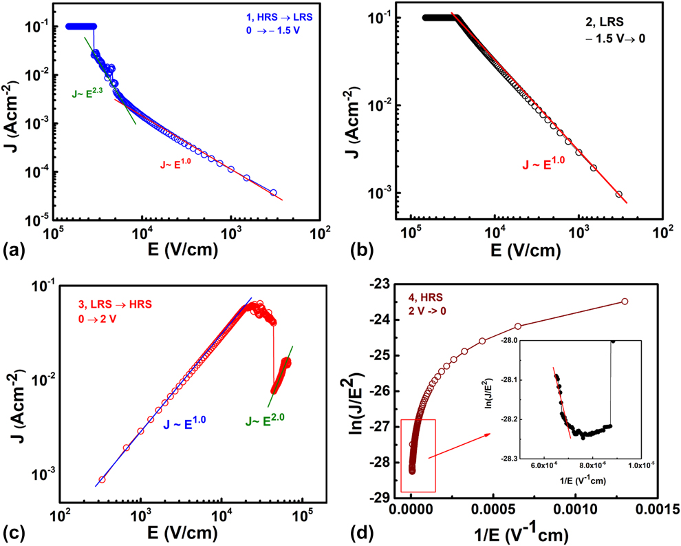
To understand the I–V characteristics in nature, electrical conduction and RS mechanisms of both devices have been studied thoroughly. Electrical conduction mechanism corresponding to the HRS and LRS of Ag/chitosan/FTO has four stages. In the first stage, from 0 to −2 V, as described above, the HRS switched to the LRS as the bias voltage was increased. As seen in Fig. 3(a), the current density followed three distinct regimes corresponding to the space charge–limited current (SCLC). Space charges in materials may arise from several sources: electrode injection of electrons and/or holes, ionized dopants in interfacial depletion regions, and accumulation of mobile ions at electrode interfaces [Reference Lin, Liu, Gong, Zhao and Huang19]. Traps may be present in the bulk material or at the interface, where they can reduce the carrier mobility [Reference Lin, Liu, Gong, Zhao and Huang19]. In the Ag/chitosan/FTO device, in the first regime, the J value increased linearly against E with a slope of 1.1, owing to internal carriers in the resistive layer; thus, it followed Ohm’s law (J Ohm ∝ V) [Reference Chiu20]. When the applied voltage increased in the second regime, the slope of the J–E curve increased abruptly to 10.3, contributing to the HRS changing to the LRS at V set ≈ −1 V. This reveals a signal of transition from the ohmic to the trap-controlled space charge–limited region (J TFL ∝ V 2), as follows:
 $${J_{{\rm{TFL}}}} = {9 \over 8}\mu \varepsilon \theta {{{V^2}} \over {{d^3}}}\quad ,$$
where ε is the static dielectric constant and θ is the ratio of the free carrier density to the total number of carriers [Reference Chiu20]. After all the traps were filled, the current was completely controlled by space charge (J ∼ V 2), confirming Child’s law with a slope of 2.7 in the final regime of the SCLC mechanism [Reference Chiu20].
 $${J_{{\rm{Child}}}} = {9 \over 8}\mu \varepsilon {{{V^2}} \over {{d^3}}}\quad .$$
Electrical conduction mechanism of Ag/chitosan/FTO: (a) trap-controlled SCLC, (b) and (c) ohmic conduction mechanism, and (d) Fowler–Nordheim tunneling mechanism.

Afterward, the current followed ohmic conduction in the sweep from −2 to 0 V, since the J–E curve showed a slope of ≈1, and corresponded to the LRS, as clearly seen in Fig. 3(b). When a positive voltage sweep was applied from 0 to 2 V, a J–E plot with a different slope was obtained, as exhibited in Fig. 3(c). The LRS was still maintained during the positive bias and the J–E curve showed a linear increase following the ohmic mechanism with a slope of 1. The final voltage sweep was applied from 2 V back to 0 V to lead to one executive cycle, as depicted in Fig. 3(d). This stage shows that the HRS was maintained from the previous stage. Experimental data reveal that the current in this stage followed the Fowler–Nordheim (F–N) mechanism, as shown below, with a negative slope for (J/E 2) ∼ −1/E:
 $$J = {{{q^2}} \over {8\pi h{\varphi _{\rm{B}}}}}E\;\exp \;\left( { - {{8\pi \sqrt {2{m^ * }} } \over {3h\left| E \right|{{\left( {{\varphi _{\rm{B}}}} \right)}^{3{\rm{/}}2}}}}} \right)\quad ,$$
where m* is the effective electron mass in the oxide, h is Planck’s constant, and φB is the junction barrier height [Reference Lim and Ismail21].
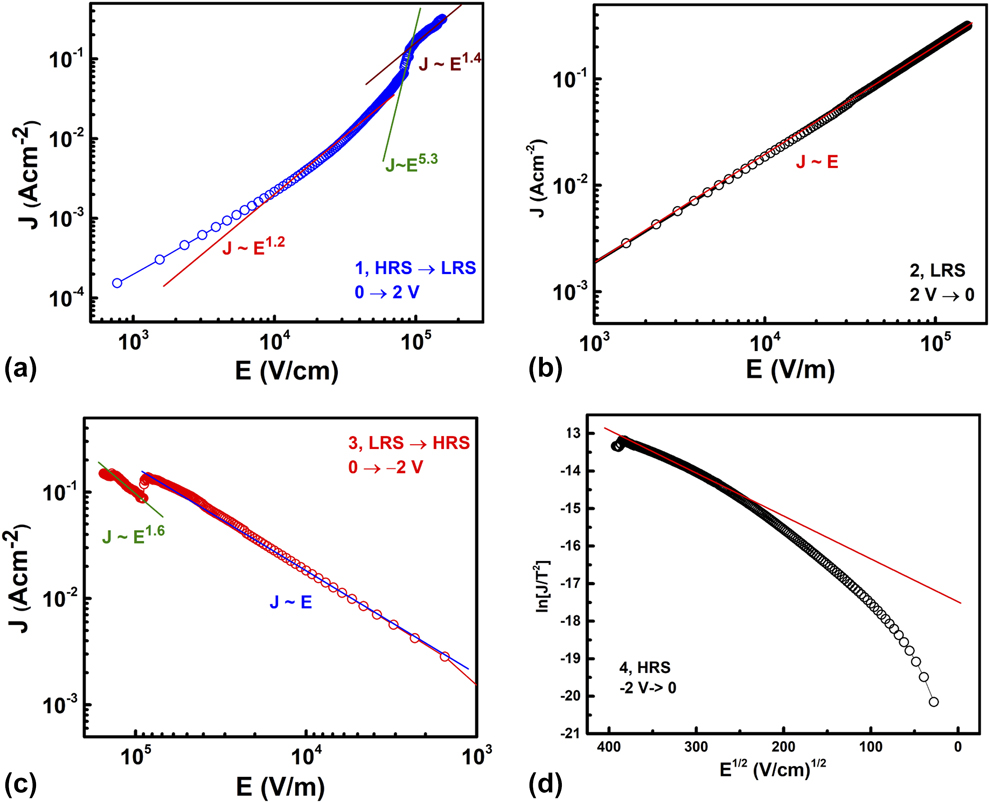
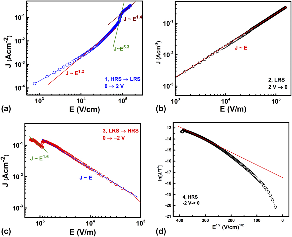
The corresponding mechanism for the Al/chitosan/FTO structure is shown in Fig. 4, which also consisted of four stages, but in the reverse direction as that of the Ag/chitosan/FTO structure. In the first stage, from 0 to 2 V, the J increased with an initial linear slope of 1.2 (J ∼ E 1.2), adhering to Ohm’s law. When the set state was formed, suggesting that the resistive state changed from the HRS to the LRS, the J increased abruptly leading to 5.3 and kept increasing slowly afterward with a decreased slope of 1.4. The J–E characteristics of the first stage indicated great dependence on three distinct terms of the applied voltage and therefore a trap-controlled SCLC mechanism similar to the mechanism of the Ag/chitosan/FTO structure. The next stage, from 2 to 0 V, occurring in the LRS, showed a linear J–E curve with a slope of 1 and followed ohmic conduction. In the third stage, from 0 V to −2 V, the low resistive mode was still retained, and the inceptive J changed linearly with E with a slope of 1. The current in the final stage from −2 to 0 V was controlled by Schottky emission (ln[J/T 2 ∼ E 1/2]), which occurred when electrons were provided enough energy to overcome the barrier at the metal/dielectric interface and entered the dielectric region. The current density due to Schottky emission followed:
 $$J = {A^*}{T^2}\;\exp \;{{ - q\left( {{\varphi _B} - \sqrt {{{qE} / {4\pi {\varepsilon _{\rm{r}}}{\varepsilon _0}}}} } \right)} \over {kT}}\quad ,$$
where A* is the effective Richardson constant, T is the absolute temperature, φB is the Schottky barrier height, E is the electric field across the dielectric, k is Boltzmann’s constant, εr is the optical dielectric constant, and ε0 is the permittivity in vacuum [Reference Chiu20].
Electrical conduction mechanism of Al/chitosan/FTO: (a) trap-controlled SCLC, (b) ohmic conduction, (c) ohmic and Ballistic mechanisms, and (d) Schottky emission.
Based on the I–V characteristics, RS reliability, and electrical conduction mechanism of Ag/chitosan/FTO, we suggest the reversible RS mechanism for this structure, as shown in Fig. 5(a). During the first stage, from 0 to −2 V, the top Ag electrode was applied a positive voltage, while the bottom one was negative biased. Electrons were injected from the bottom electrode and fill the defect sites, which exist intrinsically in chitosan film. Hereby, the current was dominated by SCLC mechanism at the first stage of I–V curve. Simultaneously, with the positive biased voltage at Ag electrode, the oxidation process happened in this side. The Ag atoms were oxidized and formed Ag+ at Ag/chitosan interface following the reaction Ag → Ag+ + e [Reference Zhou, Lu, Yao, Wang, Yang, Zhou, Li, Ding and Song22]. Ag+ cations penetrated the chitosan layer when the external electric field was high enough. Subsequently, they migrated to the FTO electrode and were reduced via the reaction Ag+ + e → Ag to generate Ag, which deposited and grew conduction filament from chitosan/FTO interface. Whenever the formation of Ag conduction filaments was completed, the resistance of device changed from the HRS to the LRS. At that time, the conduction mechanism of memory device followed Ohm’s law. The redox process occurred continuously in the next stage from −2 to 0 V and therefore the Ag filaments were maintained stably and the conduction mechanism at the LRS followed Ohm’s law. When the reverse polarity electric field from 0 to 2 V was applied, ionization of Ag at the chitosan/FTO interface led to rupture of the filaments. The disconnection between the top and bottom electrodes switched the device from the HRS to the LRS. At the final stage, when the voltage was swept from 2 to 0 V again, the Ag filament formation was interrupted and switched the device back to HRS. The current at this time was controlled by the tunneling mechanism at the Ag/chitosan interface, as shown in Fig. 5(d). The switching mechanism based on metallic filaments is common for active metal electrodes, including Ag and Cu, according to some previous reports [Reference Lin, Hao, Hu, Wang, Zang, Zhu, Du and Tang23, Reference Prakash, Sharma, Kumar and Kaur24, Reference Han, Van Le, Choi, Hong, Moon, Kim, Kim, Kim and Jang25].
(a) Forming and dissociation of Ag filaments in Ag/chitosan/FTO structure and (b) interface-controlled mechanism in Al/chitosan/FTO structure.

On replacing Ag with Al, the Al/chitosan/FTO structure showed a reversal in the RS behavior and a lower On/Off ratio compared with that of the Ag/chitosan/FTO structure. Furthermore, the endurance of this configuration was seen that it had a significant variation in HRS. For this point of view, we exclude the dominant contribution of filament conduction (neither the formation/rupture of metal filament nor the migration of oxygen, which was able to be inserted from environment) in controlling RS behavior. As reported previously, the natural formation of a thin oxide film at the metal/organic interface in air may cause effective charge injection through states near the valence band of the oxide film or lead to introduction of dopants due to charge transfer from the organic layer [Reference Kumatani, Li, Darmawan, Minari and Tsukagoshi26]. However, in this study, we intended to interpret the switching mechanism of Al/chitosan/FTO structure based on the difference barrier height under external electric field supposedly without the existence of Al2O3 formation. We suggest that, in this structure, a height barrier at the metal/organic interface can be induced under the external electric field, causing a set/reset process, as shown in Fig. 5(b). The work function of Al varies from 4.06 to 4.26 eV [Reference Hölzl and Schulte27], while the electron affinity of chitosan is 0.022 eV [Reference Ray Chowdhuri, Tripathy, Haldar, Roy and Sahu28]. Assuming that vacuum levels of Al and chitosan are aligned as one, the barrier of Al/chitosan interface is estimated from 4.06 + 0.022 = 4.082 eV to 4.26 + 0.022 = 4.282 eV. Specifically, when applying a positive voltage from 0 to 2 V to FTO, the depletion region between Al and the chitosan film narrowed and the barrier height was lowered. Therefore, the injected electrons could jump over the barrier into the dielectric layer and followed the electric field to FTO bottom electrode, increasing the current. The injection current behavior may be related to both thermionic emission and field-induced tunneling mechanism [Reference Scott29]. This current was retained during the sweep back from 2 to 0 V. Conversely, a reverse bias voltage was applied from 0 V to −2 V, the depletion region was expanded, which led to the increase in the barrier height and caused the drop in diffusion current. The current in final stage might be dependent on drift current of minor carriers, which move in the direction of electric field until the voltage swept back to 0 V again. As discussed above, the RS operation of Al/chitosan/FTO was controlled mainly by charge injection at the metal/organic interface rather than the tiny conductive filaments through the insulator layer. The interface-type RS mechanism has been also reported in hybrid organic–inorganic materials and composites [Reference Han, Van Le, Choi, Hong, Moon, Kim, Kim, Kim and Jang25]. In brief, the RS phenomenon of Ag/chitosan/FTO device was originated from the formation/rupture of Ag filament, whereas the one of Al/chitosan/FTO was owing to the variation in height barrier in the electrode/isolator interface.
Conclusions
In summary, we have developed RRAM devices based on chitosan thin films with bipolar and reversible RS characteristics. The different switching directions and switching mechanisms were confirmed for two top electrode materials—Ag and Al—used in the same biased mode. The conduction mechanism of the Ag/chitosan/FTO device involved SCLC, Ohm’s law, and Fowler–Nordheim, while SCLC, Ohm’s law and Schottky emission were involved in the mechanism of the Al/chitosan/FTO device. The RS mechanism of the Ag/chitosan/FTO device was attributed to the formation and dissolution of Ag filaments in the chitosan bulk, while an interface-controlled mechanism was proposed to elucidate the RS mechanism of the Al/chitosan/FTO device. To enhance the stability and reliability of devices and their widespread applications, use of low-cost, flexible, hybrid composites based on chitosan is highly recommended.
Experimental procedures
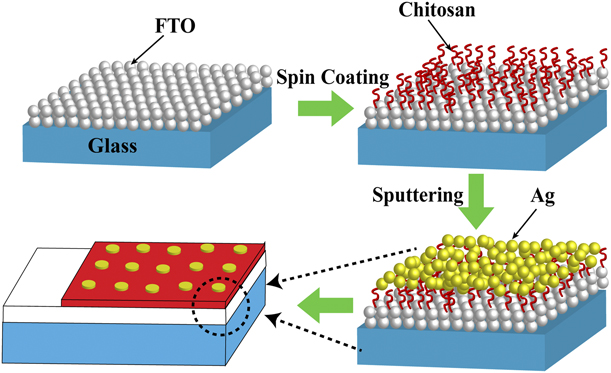
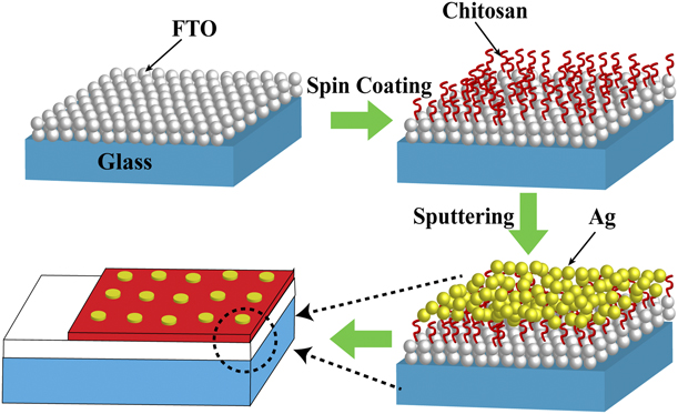
An RRAM with a metal/chitosan/FTO configuration was studied, as shown in Fig. 6. A chitosan solution (0.5 w/v) was prepared by dissolving chitosan powder (0.5 g, 99.99 in purity; Aldrich) in 100 mL of acetic acid (1 wt%), which was continuously stirred for 12 h at room temperature. A chitosan thin film was then fabricated by spin coating at 2000 rpm for 30 s. Finally, circular 100-nm-thick Ag (or Al) films were deposited by direct current (DC) sputtering technique.
Schematic diagram of Ag/chitosan/FTO memory device fabrication process.
The crystalline phases of the powder and thin films were characterized in the θ–2θ mode by a D8 Advance (Bruker) XRD with Cu Kα radiation (λ = 0.154 nm). Chemical bonding in the layers was studied by FTIR using a 4800S spectrometer (Shimadzu Corporation) working in the mid-infrared range of 400–4000 cm−1. Current–voltage (I–V) measurements were carried out using a semiconductor characterization system (Keithley 4200 SCS) and a probe station. The voltage profile for the I–V measurements was 0 V → +2 V→ 0 V → −2 V → 0 V. The bottom electrode was biased and the top electrode was grounded.
Acknowledgment
This research was funded by the Vietnam National University, Ho Chi Minh City (VNU-HCM) under Grant No. C2018-18-27.