Introduction
An optical isolator allows light waves to propagate in a specified direction and not in the opposite direction. Because of this behavior, the isolator plays an essential role in preventing undesired back reflections from interacting with optical active devices.Reference Petermann1 In an optical circulator, an optical signal input is transmitted from a first port to a second port, but an input at the second port is transmitted to a third port (rather than returning to the first port). Such functionality enables photonic circuits that process counter-propagating light waves. The demand for integrating isolators and circulators for building silicon photonic integrated circuits continues to increase.
Current optical isolators and circulators employ the Faraday effect, in which a polarization plane rotates in different directions depending on the light propagation direction. The same principle of magneto-optical polarization rotation is applicable for realizing waveguide optical nonreciprocal devices.Reference Wang, Shah and Crow2–Reference Wolfe, Fratello and McGlashan-Powell7 Note, however, that phase matching between the transverse electric (TE) and transverse magnetic (TM) modes must be realized in the waveguide to rotate the polarization. In order to achieve this, stringent control of waveguide parameters is needed to balance the various contributions to the waveguide birefringence. Although it is possible, in principle, to control the birefringence, the tolerances in the manufacturing process make it difficult to achieve the required control. In contrast, an isolator based on the magneto-optical phase shift has a distinct advantage over one based on the polarization rotation, in that it can operate in a single polarization and it is therefore not necessary to achieve phase matching between TE- and TM-mode light waves.Reference Dötsch, Bahlmann, Zhuromskyy, Hammer, Wilkens, Gerhardt, Hertel and Popkov8,Reference Levy9 TM-mode light waves experience a magneto-optical phase shift caused by first-order magneto-optical effects when they propagate in a waveguide in which a magneto-optical material (placed as an upper cladding layer) is magnetized in the film plane transverse to the light propagation direction. A different phase shift is obtained depending on the propagation direction as well as the direction of magnetization.
Another consideration in realizing optical nonreciprocal devices on a silicon waveguide platform is the integration of a magneto-optical material on silicon. In optical fiber communication wavelength bands, magneto-optical garnet (of the formula R3Fe5O12, where R is a rare-earth element) is the best candidate owing to its large first-order magneto-optical effect and low optical absorption.Reference Hansen and Krume10 However, it is quite difficult to grow garnet crystals on silicon waveguides. To overcome this, the authors developed bonding techniques for integrating a single-crystalline magneto-optical garnet on silicon.Reference Takei, Yoshida and Mizumoto11–Reference Tien, Mizumoto, Pintus, Krömer and Bowers14 In this article, we review magneto-optical nonreciprocal devices fabricated by bonding a single-crystalline magneto-optical garnet on silicon waveguides.
Deposition versus bonding
The integration of a magneto-optical material on a silicon waveguide may be achieved in two ways—deposition or bonding. Hereafter, we limit our discussion to garnet as the magneto-optical material, since it is the best candidate for optical nonreciprocal devices in the targeted wavelength band of 1550 nm. Epitaxial growth of a magneto-optical garnet on silicon has been challenging because of the large mismatch in physical properties between the garnet and silicon. The lattice constant of yttrium iron garnet (YIG), which is the most commonly used magneto-optical garnet, is 1.238 nm, whereas silicon is 0.543 nm.Reference Geller, Espinosa and Crandall15,Reference Hull16 In addition, the linear thermal expansion coefficients of YIG and silicon are 10.4 × 10⁻⁶ K–1 and 2.33 × 10⁻⁶ K–1, respectively.Reference Geller, Espinosa and Crandall15,Reference Hull16 A low-temperature process is needed for avoiding problems associated with this large difference in the thermal expansion coefficients.
Although single-crystalline magneto-optical garnet has not yet been grown on nongarnet substrates, much progress has been made in the deposition of polycrystalline magneto-optical garnets.Reference Sung, Qi and Stadler17,Reference Körner, Heinrich, Weckrle, Roocks and Stritzker18 Bi et al. succeeded in growing magneto-optical garnet on silicon using pulsed laser deposition (PLD).Reference Bi, Hu, Dionne, Kimerling and Ross19 They first deposited a thin (∼20-nm-thick) YIG seed layer on an oxidized silicon substrate at 550°C. The seed layer was subjected to rapid thermal annealing at 850°C for crystallization in the YIG phase. Subsequently, bismuth-substituted YIG [(Bi1.8Y1.2)Fe5O12, BiYIG] or cerium-substituted YIG [(Ce1Y2)Fe5O12, CeYIG] was deposited on the seed layer by PLD at 650°C. The grown BiYIG and CeYIG layers showed polycrystalline garnet phases with saturation Faraday rotations of −838 and −830° cm–1, respectively, at λ = 1550 nm. The propagation loss of the polycrystalline CeYIG layer was estimated to be ∼4 dB mm–1.
Goto et al. deposited a magneto-optical garnet having a high Faraday rotation of –3000° cm–1 at λ = 1550 nm on a silicon substrate by sputtering a sintered Ce1Y2.5Fe5Ox target.Reference Goto, Eto, Kobayashi, Haga, Inoue and Ross20 During the deposition, the substrate was held at room temperature. Thermal vacuum annealing was carried out at 800°C to crystalize the deposited garnet. Although the garnet was polycrystalline, its Faraday rotation was comparable to that of an epitaxially grown single-crystalline CeYIG. Preparing a magneto-optical garnet on silicon using deposition techniques is attractive because it enables a variety of device structures.Reference Block, Dulal, Stadler and Seaton21
Bonding techniques have advantages over deposition techniques because a single-crystalline magneto-optical garnet having a large magneto-optical constant can be prepared in a separate process and then bonded to the substrate. Tight and uniform contact between the materials is needed to obtain sufficient interaction between a light wave and the garnet. There are two options for bonding—direct bonding and adhesive bonding.
Mizumoto et al. developed a surface-activated direct bonding technique for integrating CeYIG on a silicon waveguide.Reference Mizumoto, Shoji and Takei12 The surfaces of the target wafers were activated by exposing them to a radio-frequency (RF) plasma. Subsequently, the activated surfaces were brought into contact at room temperature. While a constant pressure was applied, the sample was annealed in a vacuum chamber to obtain firm bonding. Takei et al. found that exposing wafers to oxygen or nitrogen plasma was effective for CeYIG and silicon surface activation.Reference Takei, Yoshida and Mizumoto11 The surface smoothness is a crucial issue for achieving successful bonding. Oxygen or nitrogen plasma irradiation for 10–30 s was found to be suitable for preparing the surfaces of CeYIG and silicon to a roughness of <1.0 nm.Reference Takei, Yoshida and Mizumoto11 The best strength and success rate were obtained for a nitrogen plasma exposure of 10 s and annealing at 200°C for 30 min with a pressure of 6 MPa.Reference Shoji, Itoh, Shirato and Mizumoto22
Baets et al. developed an adhesive bonding technique for integrating a variety of crystalline materials, including III–V semiconductor materials as well as CeYIG, on silicon waveguides.Reference Roelkens, Brouckaert, Van Thourhout, Baets, Nötzel and Smit13,Reference Ghosh, Keyvavinia, Van Roy, Mizumoto, Roelkens and Baets23 The technique is based on the use of a spin-coated polymer layer—divinylsiloxane-bis-benzocyclobutene (DVS-BCB)—as a bonding agent between the two materials. BCB bonding has the advantage that it is tolerant to surface relief features on either surface or small particles, with a size well below the thickness of the BCB layer. Typical thicknesses for the BCB bonding layer are in the range of 50 to 100 nm. For such layer thicknesses, the loss of confinement factor of the evanescent guided mode field in the garnet layer is limited.
Optical nonreciprocal devices based on magneto-optical phase shift
Shoji et al. gave the first demonstration of a silicon waveguide optical isolator, based on the magneto-optical phase shift in a Mach–Zehnder interferometer (MZI) configuration. CeYIG was directly bonded as an upper-cladding material on a silicon waveguide for obtaining the magneto-optical phase shift. An optical isolation ratio of 21 dB was demonstrated at a wavelength of λ = 1559 nm.Reference Shoji, Mizumoto, Yokoi, Hsieh and Osgood24
Since the isolator was fabricated with a shallow-etched rib waveguide, the device footprint was rather large due to a limited radius of waveguide curvature for constructing a MZI waveguide. Much effort has gone toward reducing the footprint and improving performance characteristics. In the following, a 500-nm-thick single-crystalline CeYIG layer grown on a (111)-oriented substituted gadolinium gallium garnet [(GdCa)3(GaMgZr)5O12, SGGG] substrate was used. Magneto-optical phase shifts of 3.7 and 4.8 mm–1 were obtained at λ = 1550 nm for 450- and 550-nm-wide silicon waveguides, respectively, when the thickness of silicon was 220 nm with a CeYIG saturation Faraday rotation of −4500° cm–1 at λ = 1550 nm.Reference Shoji and Mizumoto25
Optical isolators and circulators can be realized by installing a magneto-optical phase shifter in an MZI.Reference Auracher and Witte26 External magnetostatic fields are applied in antiparallel directions in both arms of the interferometer (Figure 1a) using a three-pole compact magnet. Different magneto-optical phase shifts are induced in the two arms, which results in a phase difference. The phase difference is set to −π/2 by adjusting the magneto-optical effect or length of the magneto-optical phase shifter. This phase difference is cancelled by a phase bias of π/2 + 2 mπ (m: integer) in the left arm. The phase bias is realized by adjusting the optical path difference between the two arms. Hence, the light wave propagating in the interferometer arms interferes constructively in the output coupler and emerges at the output port. This corresponds to the forward direction. For the backward direction, the magneto-optical phase difference changes its sign (i.e., π/2). Because the phase bias remains with a π/2 + 2 mπ phase difference, the light wave propagating in the two arms interferes destructively in the left coupler and does not emerge at the initial input port. A waveguide optical circulator is built by adopting 3-dB directional couplers as shown in Figure 1b.Reference Mitsuya, Shoji and Mizumoto27
Schematic of a silicon waveguide optical (a) isolator and (b) circulator based on the Mach–Zehnder interferometer.Reference Shoji and Mizumoto25

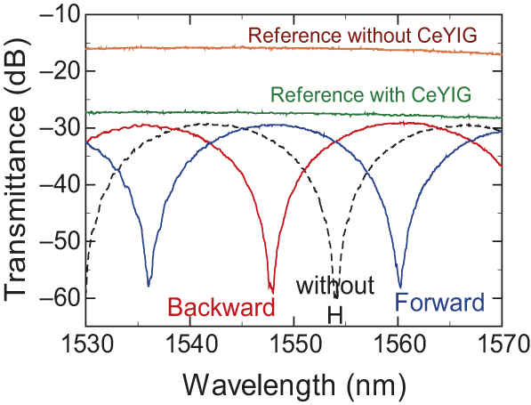
The measured fiber-to-fiber transmittance of an MZI isolator under a fixed magnetostatic field is shown in Figure 2. A comparison of the transmittances shown by the blue and red lines, which correspond to counter propagating directions, reveals that the transmittance differs depending on the light propagation direction. The maximum isolation ratio, which is defined as the transmittance ratio of the forward to the backward direction, is measured to be 30 dB at λ = 1548 nm. The isolation bandwidth can be increased by properly designing the phase bias.Reference Shoji and Mizumoto28,Reference Shoji, Shirato and Mizumoto29
Measured fiber-to-fiber transverse magnetic-mode transmittance of the Mach–Zehnder interferometer silicon waveguide optical isolator fabricated by directly bonding a Ce-doped yttrium iron garnet (CeYIG) cladding layer. Blue and red lines show the transmittances corresponding to two counter-propagation directions; the broken line is that of a nonmagnetized device (without H). Green and orange lines show the fiber-to-fiber transmittance of reference waveguides with and without a CeYIG cladding layer, respectively.Reference Shoji and Mizumoto25

In practical applications, athermal operation is important. The temperature dependence of an MZI isolator is determined mainly by the temperature dependence of the refractive indices of the constituent materials and of Faraday rotation of the magneto-optical garnet. Furuya et al. measured these temperature dependences of CeYIG.Reference Furuya, Nemoto, Kato, Shoji and Mizumoto30 By balancing the temperature dependence of the magneto-optical phase shift and phase bias in the backward direction, they demonstrated the constant backward transmittance of an MZI-based isolator at temperatures between 20 and 60°C.
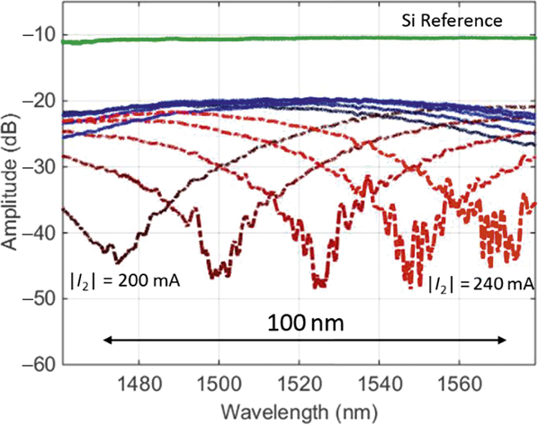
Huang et al. recently demonstrated that the bulky magnet used in these magneto-optical devices can be effectively replaced with an integrated electromagnet.Reference Huang, Pintus, Zhang, Shoji, Mizumoto and Bowers31 The proposed solution combines the advantage of minimizing the footprint and tuning the transmission bandwidth of the isolator (or circulator).Reference Huang, Pintus, Shoji, Morton, Mizumoto and Bowers32 Figure 3 shows the performance of an MZI-based isolator with an integrated electromagnet, where more than 20 dB of optical isolation is achieved within a 18-nm-wide optical bandwidth. At the same time, the central operating wavelength of the isolator can be tuned across 100 nm.
Measured forward (blue) and backward (red) spectra for a bonded Ce-doped yttrium iron garnet Mach–Zehnder interferometer isolator as the tuning current (I 2) is changed, demonstrating tuning more than 100 nm.Reference Huang, Pintus, Shoji, Morton, Mizumoto and Bowers32

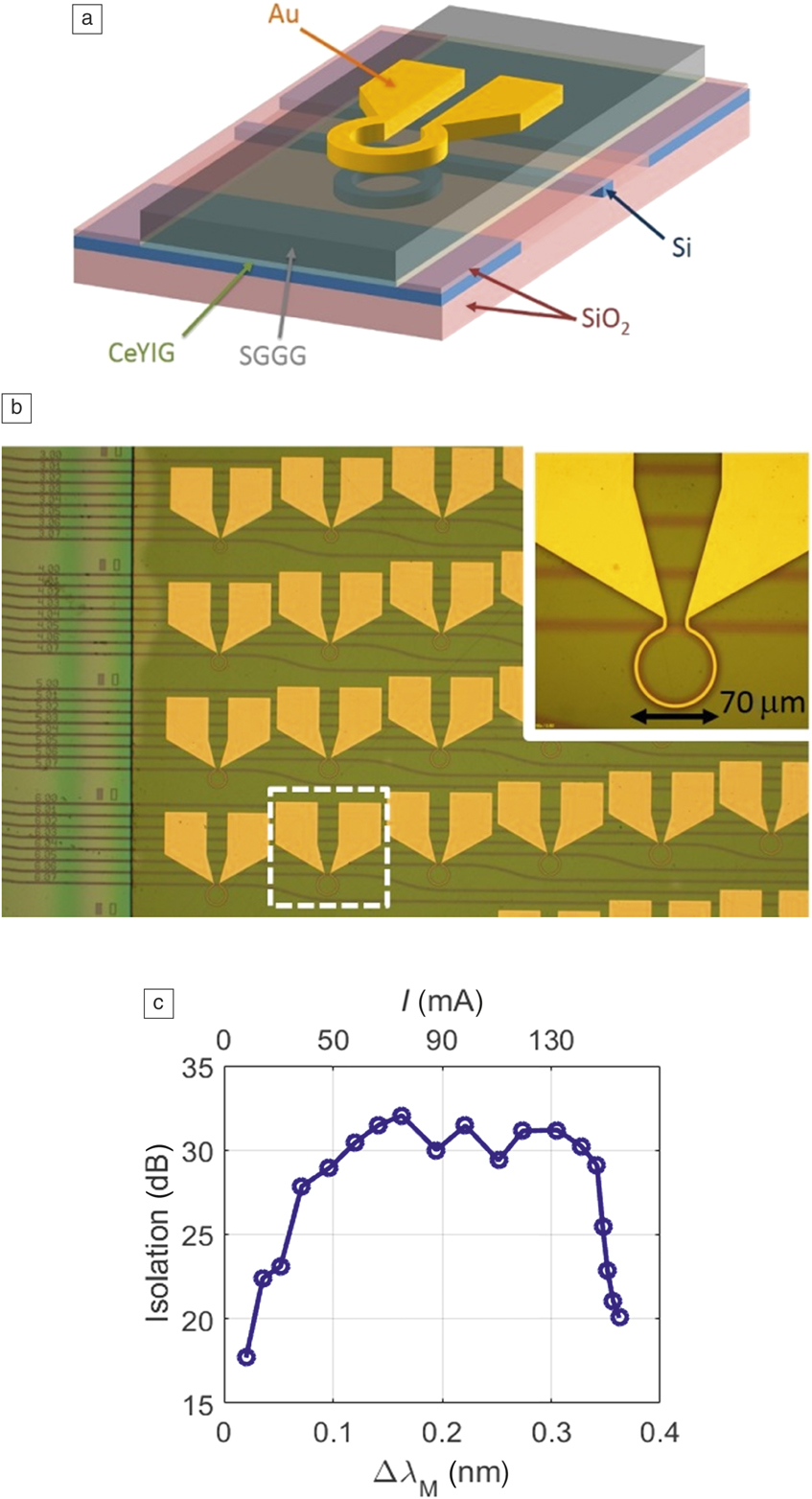
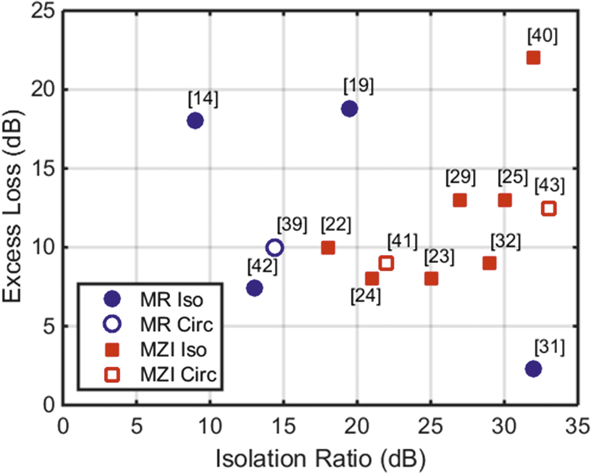
An integrated optical isolator has been also demonstrated by exploiting a ring resonator architecture, as shown in Figure 4.Reference Tien, Mizumoto, Pintus, Krömer and Bowers14,Reference Kono, Kakihara, Saitoh and Koshiba33–Reference Pintus, Huang, Zhang, Shoji, Mizumoto and Bowers36 When a ring resonator includes a magneto-optical phase shifter, a light wave propagating in the resonator has a direction-dependent optical path length. The resonant wavelengths of clockwise- and counterclockwise-propagating light waves become different.Reference Tien, Mizumoto, Pintus, Krömer and Bowers14 The smaller footprint of the ring isolator allows higher integration and reduction of the insertion losses of the MZI isolator. The array of 24-ring resonator isolators shown in Figure 4b covers an area the size of one MZI isolator. An integrated electromagnet can provide the necessary magnetic field for both ring and MZI-type architectures. Tuning of the isolator using the electromagnet is shown in Figure 4c; the isolation can be high (>30 dB) over a broad current range, which can be used to achieve athermal operation. Figure 5 summarizes the losses and isolation achieved to date with microring and Mach–Zehnder-based isolators and circulators.
(a) Schematic diagram of a ring resonator isolator. (b) Photograph of an array of 24-ring resonator isolators; inset shows detail of one isolator. (c) Optical isolation as a function of the current (I, top axis) and the nonreciprocal resonance wavelength split (ΔλM, bottom axis). Note: SGGG, substituted gadolinium gallium garnet.

Loss and extinction ratios of different isolators and circulators. Nonresonant (Mach–Zehnder interferometer [MZI]) and resonant microring (MR) devices are shown.

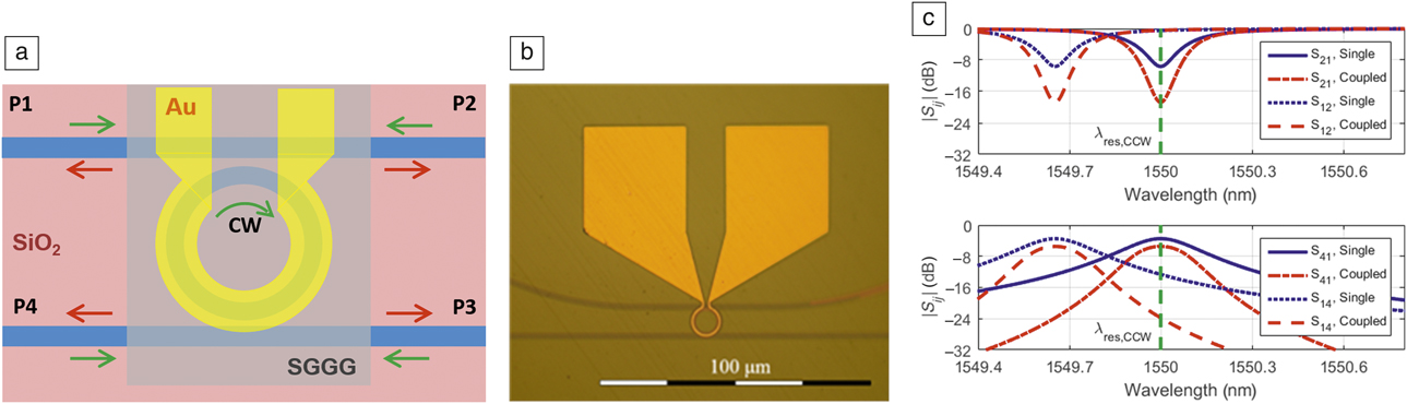
Resonators with add-drop directional couplers will perform as four-port circulators, as shown schematically in Figure 6a and in the photograph in Figure 6b.Reference Pintus, Di Pasquale and Bowers37,Reference Jalas, Petrov and Eich38 The performance of single and cascaded resonators is compared in Figure 6c, where the improved filtering and isolation of cascaded designs is evident. The advantage of using current to generate the magnetic field is that the direction of the magnetic field, and thus the circulation direction, can be adjusted to be either clockwise (one to two to three to four to one) or counterclockwise (one to four to three to two to one). If additional rings are added in a ring-bus-ring configuration, six- and eight-port circulators can be made. If the integrated electromagnet is used, then the circulation patterns can be reconfigurable.Reference Huang, Pintus, Zhang, Morton, Shoji, Mizumoto and Bowers39 These isolators and circulators work with TM polarization and utilize CeYIG bonded over Si waveguides. Pintus et al. describe combinations of CeYIG with Si3N4 waveguides to allow isolators and circulators to be made in both TE and TM configurations.Reference Pintus, Di Pasquale and Bowers37
(a) Schematic structure of the transverse magnetic-mode four-port optical circulator showing input and output signals at each port, and (b) optical micrograph of the fabricated four-port circulator. (c) Wavelength dependence of single- and two-microring circulators. Note: SGGG, substituted gadolinium gallium garnet; CW, clockwise; λres,CCW, resonant wavelength of light propagating in the counterclockwise direction; S ij, fraction of power transmitted from port i to port j.

All of the devices described so far were demonstrated with direct bonding of magneto-optical materials on silicon. Ghosh et al. realized bonding of CeYIG on silicon waveguides by using BCB as an adhesive polymer.Reference Ghosh, Keyvavinia, Van Roy, Mizumoto, Roelkens and Baets23 After aligning a 4 × 4 mm2 CeYIG die on a silicon waveguide, they applied a curing process for approximately 3 h. An MZI silicon waveguide optical isolator fabricated by bonding a CeYIG die with a BCB adhesive layer demonstrated a maximum isolation ratio of 25 dB for a fundamental TM mode at λ = 1495.2 nm. They also demonstrated an isolator that worked for a TE-mode input.Reference Ghosh, Keyvaninia, Shirato, Mizumoto, Roelkens and Baets40 Because only TM modes experienced the magneto-optical phase shift in the waveguide with a bonded magneto-optical upper cladding layer, they integrated TE–TM mode converters at the input and output ports of magneto-optical phase shifters. A maximum isolation ratio of 32 dB was obtained at λ = 1540.5 nm. Finally an optical circulator was demonstrated by terminating one of the ports of the MZI structure with a reflector.Reference Ghosh, Keyvaninia, Van Roy, Mizumoto, Roelkens and Baets41
Conclusions
Optical nonreciprocal devices fabricated by bonding a magneto-optical garnet on silicon waveguides have been reviewed in this article. The bonding technique is advantageous compared with state-of-the-art deposition techniques, since a single-crystalline magneto-optical garnet having a high Faraday rotation can be used. The devices discussed in this article employ a magneto-optical phase shift in a MZI or a ring resonator. MZI silicon waveguide isolators and circulators exhibit an isolation ratio of ≥30 dB at a 1550-nm-wavelength band. Also, using an adhesive bonding technique, an MZI-based TE mode isolator was demonstrated with an isolation ratio of 32 dB. The isolation bandwidth of an MZI-based device can be increased by properly setting a phase bias. An MZI-based isolator having a temperature-independent backward transmittance was realized by balancing the temperature dependence of the magneto-optical phase shift and phase bias. An integrated electromagnet can also be incorporated on chip providing wavelength tuning capabilities, and further reducing the footprint. In future work, the insertion loss of isolators and circulators must be reduced. Also, integrating isolators with lasers and other optical active devices is needed.
Acknowledgments
This work was supported by the JST Core Research for Evolutional Science and Technology (CREST) No. JPMJCR15N6 and by the DARPA IPHOD contract and Air Force Small Business Innovation Research (SBIR) funding through Morton Photonics (FA8650–16-C-1758).

Tetsuya Mizumoto has been Vice President for Education at the Tokyo Institute of Technology (Tokyo Tech), Japan, since 2012. He received his Doctor of Engineering degree in electrical and electronic engineering in 1984 from Tokyo Tech, and was promoted to full professor in the Graduate School of Engineering in 2004 prior to his present position. His research focuses on waveguide optical devices, especially magneto-optical devices and all-optical switching devices. He was awarded the IEEE Photonics Society Distinguished Lecturer Award in 2009, IEEE Fellow in 2012, and the IEICE Achievement Award in 2012. Mizumoto can be reached by email at tmizumot@pe.titech.ac.jp.

Roel Baets has been a professor in the faculty of engineering and architecture of Ghent University (UGent), Belgium, since 1989. He received his PhD degree from UGent in 1984. He has also held faculty positions at Delft University of Technology and Eindhoven University of Technology, The Netherlands. His research group is associated with the Interuniversity Microelectronics Centre, Belgium. His research focuses on the field of integrated photonics, in particular, silicon photonics, and its applications in telecom, datacom, sensing, and medicine. He is an ERC grantee of the European Research Council. He is a Fellow of the IEEE, of the European Optical Society and of The Optical Society (OSA). Baets can be reached by email at roel.baets@ugent.be.

John E. Bowers is director of the Institute for Energy Efficiency and a professor in the Departments of Electrical and Computer Engineering and Materials at the University of California, Santa Barbara (UCSB). He received his MS and PhD degrees from Stanford University. He worked for AT&T Bell Laboratories and Honeywell before joining UCSB. His research interests focus on silicon photonics, optoelectronic devices, optical switching, and transparent optical networks and quantum dot lasers. He is a Fellow of the IEEE, The Optical Society (OSA), and the American Physical Society, and a recipient of the IEEE Photonics Award, OSA/IEEE Tyndall Award, the IEEE LEOS William Streifer Award, and the South Coast Business and Technology Entrepreneur of the Year Award. He is a member of the National Academy of Engineering and the National Academy of Inventors. Bowers can be reached by email at bowers@ece.ucsb.edu.