I. INTRODUCTION
Metal oxide semiconductor films have been widely studied and have received considerable attention in recent years due to their optical and electrical properties. Zinc oxide (ZnO) films are promising candidates for use in optoelectronic devices. ZnO is one of the best options as transparent conductive thin-film electrodes for silicon-based thin-film solar cells due to its high chemical stability against reducing environments,Reference Ortız, Sanchez, Falcony, Farıas, Hirata and Cota-Araiza1 a textured surfaceReference Martinez, Herrero and Gutierrez2 and the simultaneous concurrence of high transparency in the visible region, and a high conductivity.Reference Oktik3 The deposition of high-quality ZnO thin films is reported using a wide variety of techniques, such as reactive evaporation,Reference Zhao, Hu, Wang, Zhao, Liang and Wang4 sputtering,Reference Song, Watanabe, Kon, Mitsui and Shigesato5 chemical vapor deposition,Reference Hu and Gordon6 spray pyrolysis,Reference Krunks and Mellikov7 sol–gelReference Schuler and Aegerter8 and electrochemical deposition.Reference Marotti, Guerra, Bello, Machado and Dalchiele9 ZnO has recently gained much interest because of its potential use in many applications, ranging from antireflection coatings, transparent electrodes in solar cells,Reference Kluth, Schöpe, Hüpkes, Agashe, Müller and Rech10 thin-film gas sensors,Reference Shishiyanu, Shishiyanu and Lupan11 varistors,Reference Suvaci and Özer12 spintronic devices,Reference Meron and Markovich13 photodetectors,Reference Liang, Sheng, Liu, Huo, Lu and Shen14 surface acoustic wave devices,Reference Emanetoglu, Gorla, Liu, Liang and Lu15 and light-emitting diodesReference Saito, Haneda, Sekiguchi, Ohashi, Sakaguchi and Koumoto16 to nanolasers.Reference Huang, Mao, Feick, Yan, Wu, Kind, Weber, Russo and Yang17 Its usefulness is attributed to its wide and direct band gap, excellent chemical and thermal stability, and specific electrical and optoelectronic property of being a II–VI semiconductor with a large exciton binding energy.
ZnO is both transparent in the visible region and electrically conductive especially when doped with appropriate metals, such as indium, gallium, or aluminum. It is well known that chemical doping greatly influences the electronic and optical properties of ZnO. Doped ZnO thin films are of technological importance because of their great potential for various applications, such as transparent conducting electrodes (doping with III A elements)Reference Kluth, Schöpe, Hüpkes, Agashe, Müller and Rech10,Reference Pearton, Norton, Ip, Heo and Steiner18 for flat panel displays, solar cells, optoelectronic devices, electrochromic devices, etc., insulating or dielectric layers (doping with Li),Reference Hiramatsu, Imaeda, Horio and Nawata19 and spintronic devices (doping with Mn).Reference Meron and Markovich13 Among the various doped ZnO films, aluminum (Al)-doped zinc oxide (AZO) films have drawn considerable attention for transparent conducting electrodesReference Pearton, Norton, Ip, Heo and Steiner18 due to its high conductivity and good optical transmittance. ZnO is an n-type wide band gap semiconductor (3.3 eV), and its electrical conductivity is due to intrinsic (zinc excess at the interstitial position and the lack of oxidation) and extrinsic defects. The conductivity of pure ZnO is due to the former defects. As pure ZnO thin films are sensitive to oxidation, absorption of O in the films is inclined to decrease the electrical conductivity. In case of doped ZnO, the electrical properties are enhanced by extrinsic defects. Additionally, electrical properties of ZnO could be modified by thermal treatment in a reducing atmosphere.
ZnO normally forms in the hexagonal structure with a = 3.25 Å and c = 5.12 Å; each Zn atom is tetrahedrally coordinated to four O atoms, where the Zn d-electrons hybridize with the O p-electrons; layers occupied by zinc atoms alternate with layers occupied by oxygen atoms.Reference Joseph, Tabata and Kawai20 ZnO:M (M = Al, Ga, and In) thin films with high c-axis-oriented crystalline structure along the (002) plane are extensively studied for practical applications, including transparent conducting electrode materials for various electronic devices, such as solar cells, electroluminescence displays, etc. A high degree of crystal orientation reduces the electrical resistivity due to an increase in carrier mobility by reducing the probability of the scattering of the carriers at the grain boundary. The sol–gel method is widely used to obtain various kinds of functional oxide films, including ZnO and doped ZnOReference Xu, Deng, Li and Cheng21,Reference Kuo, Chen, Lai, Cheng, Kuo, Wang and Hsieh22 thin films with preferred c-axis orientation. Aluminum is a promising dopant to improve the optoelectrical properties of ZnO films.
In the present study, we have investigated the influence of different aluminum contents on the structural, electrical, optical, and morphological characteristics of aluminum-doped ZnO films deposited on Si wafers and microslide glass substrates using the sol–gel technique. The sol–gel method is adopted in this work as it provides excellent compositional control, homogeneity on the molecular level, and lower crystallization temperature.
II. EXPERIMENTAL
A. Preparation of precursor sol
Initially, diethanolamine (sol stabilizer) is dissolved in ethanol. To this solution, zinc acetate dihydrate is added and stirred for duration of 15 min. The molar concentration of zinc acetate dihydrate in the solution was 0.3 M. Doping of the above solution by aluminum was carried out by adding to it aluminum nitrate nonahydrate such that the atomic ratio of Al:Zn = 0.05, 0.1, 0.2, and 0.3. The resulting solutions became clear and homogeneous after stirring for 15 min. Furthermore, the advantage of using diethanolamine (a solvent with high boiling point) as the sol stabilizer arises from the fact that it results in transparent ZnO films with strongly preferred orientation.
B. Deposition of thin films
The films have been deposited using the spin-coating technique at 1500 rpm for duration of 30 s on polished silicon wafers and microslide glass substrates, which were thoroughly cleaned prior to the coating. The films thus obtained were thermally treated in a conventional furnace at a temperature of 500 °C for duration of 5 min. Transparent homogeneous films having good adherence with the substrates and excellent chemical and mechanical stability were obtained.
C. Characterization of thin films
X-ray diffraction (XRD) patterns of the films have been recorded in the 2θ range from 20 to 80° with a D8 Advanced Bruker diffractometer (Karlsruhe, West Germany). Fourier transform infrared (FTIR) spectra of the films in reflection mode were recorded in the wave number range of 400–4000 cm−1 on a Perkin-Elmer Model BX2 Spectrophotometer. The surface morphology of the films has been observed using scanning electron microscopy (SEM) on a JEOL JSM 840 scanning electron microscope (Nagoya, Japan). The energy dispersive x-ray analysis has been performed on Oxford Link Isis 300 (Cambridge, UK). Atomic force microscopic images for the films were obtained on a Nanoscope II instrument. Optical transmittance and reflectance data of the films have been measured in the range of 300–1100 nm using a UV 3101 PC Shimadzu spectrophotometer (Kyoto, Japan). Electrical characteristics of the films have been measured using the four-probe method.
III. RESULTS AND DISCUSSION
A. X-ray diffraction
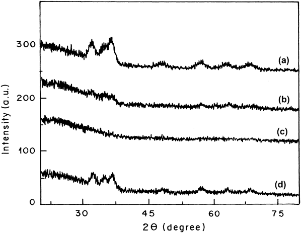
Figure 1 shows the XRD patterns of the AZO films with different aluminum contents and annealed at 500 °C. The crystallite size in the films was observed to lie in the nano range between 5.7 and 11.4 nm. The XRD patterns in general have exhibited higher degree of crystallinity. The crystalline phase present in these films is identified as the hexagonal wurtzite structure of ZnO as per PDF file no. 36-1451. In the Al:Zn (0.05, 0.2, and 0.3) films, the Bragg peaks corresponding to hexagonal ZnO appear at 2θ = 32.2, 34.8, 36.6, 47.6, 56.9, 63.3, and 68.6° from the (100), (002), (101), (102), (110), (103), and (112) reflections, respectively. Importantly, a preferred orientation is seen along the (101) plane in the Al:Zn (0.05, 0.2, and 0.3) films. It is noteworthy that the nature of the Al:Zn (0.1) film is slightly different owing to the absence of peaks that are present in all other samples under investigation. This shows that Al:Zn (0.1) content in the samples has induced in them some distinctive features. Further increase in Al content from 0.2 to 0.3 has caused a narrow broadening of the dominant Bragg peaks of hexagonal ZnO, which is consistent with the decreasing crystallinity of the sample. The crystallite sizes in the films as estimated from the Debye Scherrer's formula are found to lie in the nano range, i.e., the films exhibit both amorphous and crystalline characteristics. From the XRD investigation, it is found in our earlier workReference Verma, Khan, Kumar, Kar, Chakravarty, Singh and Husain23 that for the Al:Zn (0.2) films, preferential growth of (100) reflection peak has taken place in the 450, 550, and 600 °C annealed films.
XRD patterns of the AZO films with different aluminum contents annealed at 500 °C. (a) 0.3, (b) 0.2, (c) 0.1, and (d) 0.05.

B. Fourier transform infrared investigation
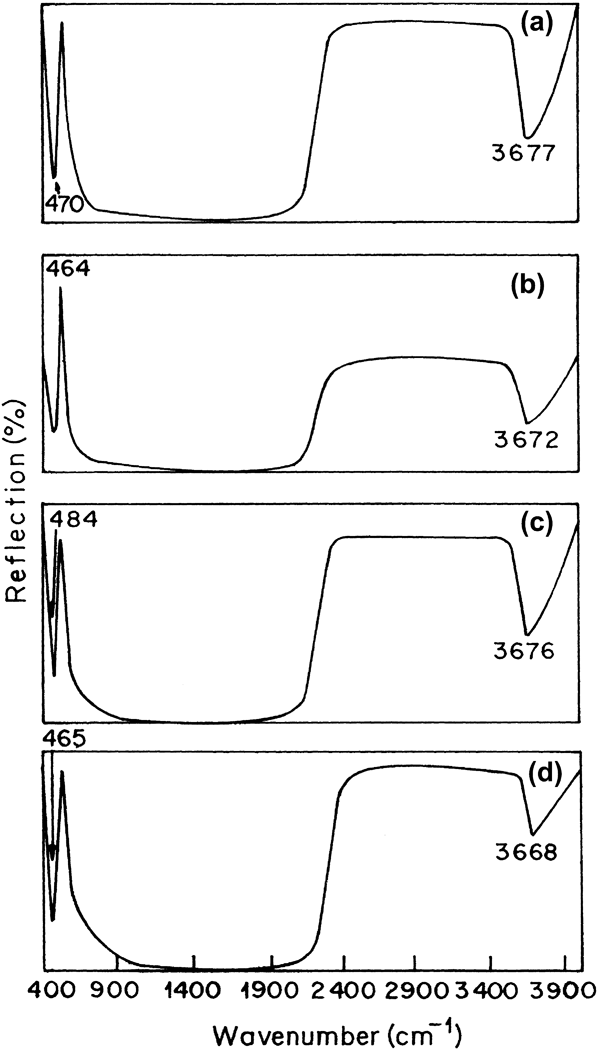
Figure 2 shows the FTIR spectra of the AZO films with different aluminum contents and annealed at 500 °C. The films exhibit absorption bands assigned to Zn–O stretching vibration at 465 cm−1. The films also exhibit a broad absorption band near 3600 cm−1 assigned to O–H stretching vibration. The presence of absorption band assigned to O–H stretching vibration shows that the films contain chemisorbed and physisorbed water.
FTIR spectra of the AZO films with different aluminum contents annealed at 500 °C. (a) 0.3, (b) 0.2, (c) 0.1, and (d) 0.05.
C. Morphological properties
1. Scanning electron microscopy and atomic force microscopy
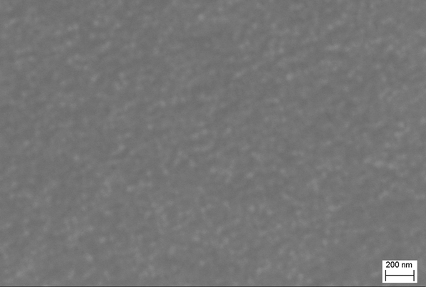
The SEM micrograph of the film with Al:Zn (0.2) is illustrated in Fig. 3. The films are constituted of fine grains, which agglomerate to form uniformly distributed large interconnected round clusters (polycrystalline grains). This study has revealed that the films under investigation are highly dense and compact in nature, i.e., these samples in general exhibit lower degree of porosity. These films have demonstrated the presence of closely packed polycrystalline grains. The morphology of the films with higher Al content as seen by SEM was, however, found to be granular and porous. The size of polycrystalline grains in the Al:Zn (0.2) films is nearly 25 nm. In the Al:Zn (0.3) film, however, these grains are interconnected, and therefore, these grains are much larger in size in the same sample. Also, in general, it is seen that the surface structure of the films is dense in nature irrespective of the Al content. It has been observed that with increasing Al content in the films, the size of polycrystalline grains and the size of pores increases. On an average, the grain size varies from 25 to 50 nm. Importantly, it has been observed by other research groups that the surface morphology of the films affect their optical properties significantly. In addition, the energy dispersive x-ray analysis has shown that the atomic ratio of Al:Zn in the solutions and in thin films has similar values. Scanning electron microscopic study for the Al:Zn (0.2) films in our earlier workReference Verma, Khan, Kumar, Kar, Chakravarty, Singh and Husain23 has shown that the films contain well-defined grains arranged in a closely packed array.
SEM image of the AZO film with the Al content of 0.2 annealed at 500 °C.
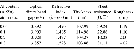
The AFM image of the Al:Zn (0.2) thin film is shown in Fig. 4. The roughness values of the different films as evaluated from the AFM images are shown in Table I. The low roughness value of the films shows that the sample surface is relatively smooth in all the films under investigation.
AFM image of the AZO film with the Al content of 0.2 annealed at 500 °C.
Optical direct band gap, refractive index, thickness, sheet resistance, and roughness of the films with different Al contents.
D. Optical properties
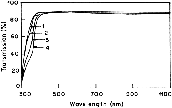
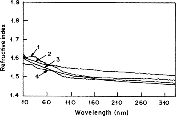
The transmittance of AZO films with different aluminum contents in the wave length range of 300–1100 nm are shown in Fig. 5. The transmission spectra of the films in the entire visible region is observed to be excellent. The transmittance of the films was found to be in the range of 85–90% in the entire UV-visible-near infrared region. The thickness of the films was determined to lie in the range of 103–115 nm. The refractive index was observed to be in the range of 1.47–1.53 at 600 nm. The refractive indices of the different AZO thin films as a function of wave length are shown in Fig. 6. The refractive indices and thickness of the films with different Al contents are shown in Table I.
Transmission spectra of AZO films with different aluminum contents in the wave length range of 300–1100 nm. (1) 0.3, (2) 0.2, (3) 0.1, and (4) 0.05.
Refractive indices of the different AZO thin films as a function of wave length. (1) 0.3, (2) 0.05, (3) 0.2, and (4) 0.1.
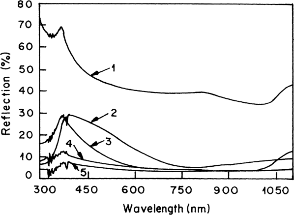
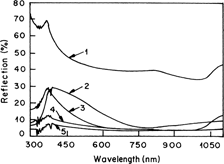
The reflection spectra of the AZO films with different aluminum contents deposited on Si wafers are shown in Fig. 7. A bare silicon wafer has a reflectivity value of nearly 35%. The reflectivity of the films was found to lie in the range of 3–13% at 600 nm. These AZO films seem highly suitable for application as antireflecting coating to silicon solar cells. The deposition of AZO coatings on Si wafers has reduced the reflectivity to a value as low as 3%. Also, the reflectivity spectra reveal that with increasing wave length from 400 to 1100 nm, the reflectance is low in the entire wave length region. The measured values of n satisfy the first condition of antireflection coating for Si solar cells, viz., n 1 ≅ n Si1/2. The thickness of the films deposited at 1500 rpm for duration of 30 s is measured to be about 100 nm. The thickness is also nearly appropriate to cause destructive interference after reflection from front emitter of solar cells.
Reflection spectra of the AZO films with different aluminum contents deposited on Si wafers. (1) Bare silicon wafer, (2) 0.1, (3) 0.2, (4) 0.3, and (5) 0.05.
The optical direct and indirect band gaps of these films have also been calculated. For a transparent thin film, the absorption coefficient per unit length (α) is determined from its transmittance (T), i.e.,
 $${\rm{\alpha }} = \ln (1/T)/d\quad ,$$
where d is the film thickness. If the film is semiconducting, a relationship exists between α and energy band gaps (E g) for direct and indirect transitions. It follows that
 $$A/d = {\rm{\alpha }} = {(h{\rm{\nu }} - {\rm{ }}{E_{\rm{g}}})^{\rm{\gamma }}}\quad ,$$
where A is the absorption coefficient, γ = 1/2 for direct, and γ = 2 for indirect transitions.
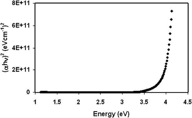
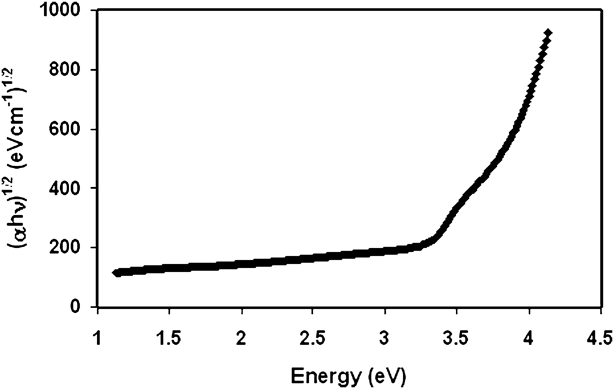
According to Eqs. 1 and 2, by extrapolating the linear part of a curve of A 1/2 versus photon energy or A 2 versus photon energy to the abscissa, the energy band gaps for indirect and direct transitions can be derived. The direct band gap (Fig. 8) of the Al:Zn (0.2) film is found to be 3.93 eV. The indirect band gap (Fig. 9), however, for the same film is measured to be 3.57 eV. It is known from the literature that the band gap of ZnO films can increase upon the addition of dopants. The direct band gap of the films was found to increase from 3.89 to 3.93 eV as the Al:Zn content was increased from 0.05 to 0.2. However, the band gap was observed to decrease to 3.86 eV for the Al:Zn (0.3) thin film. Table I shows the optical direct band gap of the films with different Al contents. In our previous work for the Al:Zn (0.2) thin films annealed at 500 °C,Reference Verma, Khan, Kumar, Kar, Chakravarty, Singh and Husain23 we have shown that the films have exhibited excellent optical transmittance (∼90%) in the wave length range of 400–1100 nm. In addition, refractive indices (n = 1.9–1.95) of the filmsReference Verma, Khan, Kumar, Kar, Chakravarty, Singh and Husain23 on Si wafers are independent of the annealing temperature. Thickness of the films produced at 4000 rpm is in the range of 58–62 nm.Reference Verma, Khan, Kumar, Kar, Chakravarty, Singh and Husain23 Moreover, the films have demonstrated a reflectivity value of about 3% at a wave length of 700 nm.Reference Verma, Khan, Kumar, Kar, Chakravarty, Singh and Husain23
Direct band gap evaluation of the AZO thin film with an Al content of 0.2.
Indirect band gap evaluation of the AZO thin film with an Al content of 0.2.
E. Electrical properties
Resistivity of the AZO films has been measured using the four-probe method. The electrical resistivity of the Al:Zn (0.2) film is calculated to be around 1.78 × 10⁻⁴ Ω cm. In our earlier work, we have reported the resistivity of the 500 °C annealed Al:Zn (0.2) film to be 5 × 10⁻¹ Ω cm. The lower value of resistivity attained in the present work is an outcome of the different molar concentrations of the solutions used for the preparation of the thin films. Polished silicon wafers is found to exhibit a sheet resistance of 30–35 Ω/□. The deposition of Al:Zn (0.2) AZO thin film on Si wafers reduced its sheet resistance from 30 to 10 Ω/□. This result shows that the Al:Zn (0.2) AZO film is conducting in nature. This shows that the Al:Zn (0.2) AZO film can be used as a transparent conducting coating also as the coating is both transparent and electrically conducting. The highly dense structure of these films has bestowed them with low resistivity values. The electrical conductivity of AZO films is mainly due to extrinsic defects. The sheet resistance of the films with different Al contents is shown in Table I.
IV. CONCLUSIONS
Sol–gel-derived polycrystalline Al-doped ZnO thin films have been deposited on polished Si wafers and microslide glass substrates using a precursor sol containing zinc acetate dihydrate, aluminum nitrate nonahydrate, diethanolamine, and ethanol using the spin coating technique. The effect of varying the aluminum content on structural, optical, morphological, and electrical characteristics has been examined in the present work. The SEM study has shown that the films contain well-defined polycrystalline grains, which are arranged in a closely packed arrangement. Among all the studied films, the Al:Zn (0.05) film has exhibited the most dense surface structure. Importantly, due to their compact structure, the films have exhibited low resistivity (1.78 × 10⁻⁴ Ω cm). As determined from the SEM micrographs, the polycrystalline grain size in the films is in the range of 25–50 nm. XRD studies have shown preferential orientation in the films along the (101) plane. The films have exhibited excellent optical transmittance (∼90%) in the visible region. Direct band gap of the films is measured to be 3.93 eV. The refractive indices (n = 1.47–1.53) of the films on microslide glass substrate as measured by a spectroscopic ellipsometer are nearly independent of varying the aluminum content. Thickness of the films is in the range of 103–115 nm. The films are characterized by a reflectance of about 3–13% at a wave length of 600 nm. The films have shown a constant low value of reflectivity as a function of wave length. The reflectivity of the films is found to be independent of wave length. The low reflectivity in the films and the appropriate values of refractive index and thickness shows the suitability of the films as antireflection coating in silicon solar cells. The best optimum features of Al:Zn (0.2) thin film proves that this composition is exhibiting the most conducive results for utility as a transparent conducting coating as well as an antireflection coating in silicon solar cells.
ACKNOWLEDGMENTS
Financial support from Council of Scientific & Industrial Research (AV) is gratefully acknowledged. The authors also wish to thank Dr. S.K. Srivastava for electrical measurements.