Introduction
The ultra-wideband (UWB) communication technology is a blessing for the short-range communication systems due to its inherent high data rate capacity (≈1 Gb/s for <10 m) and non-interfering characteristics (low output power, −41.3 dBm/MHz) [1]. However, because of its ultra-wide bandwidth, it is prone to interference from other RF sources such as WLAN, C, X, band, etc., pocketed within the UWB spectrum, and might affect its performance considerably. To overcome these drawback researchers conceptualized and conceived UWB filters possessing integrated bandstop characteristics. These filters possess single or multiple bandstop characteristics depending upon the environment. Here we concentrate our design on UWB-bandpass filters (BPF) with dual notched band characteristics and the UWB literature is replete with such filters [Reference Wu and Chen2–Reference Ghazali and Singh12].
Slots etched in microstrips on the top plane develop dual notches in [Reference Wu and Chen2, Reference Chu and Huang3], whereas structures coupled to the microstrips on a top plane in the form of electromagnetic bandgap structure (EBG), simplified composite right/left-handed resonator, E-shaped resonator, and stepped impedance resonator (SIR) develop multiple notches in [Reference Liu4–Reference Wei8], respectively. The structures proposed in [Reference Song and Xue9, Reference Mohammadi10] develop dual notches based on wave cancellation method, whereas the use of defected ground structures (DGSs) inculcate dual passband notches in [Reference Ghazali and Singh11–Reference Song, Yang and Geyi13]. UWB filters with more than two notches have been reported in [Reference Ghazali and Pal14, Reference Ghazali and Pal15]. However, most of the structures reported are quite large in size.
Here we propose a compact UWB-BPF with dual passband notches. The basic topology of our UWB filter is based on broadside coupled technology of microstrip-to-CPW, conceptualized in [Reference Baik, Lee and Kim16]. The basic structure of our proposed UWB filter consists of microstrips on a top plane arranged in a back-to-back manner, which are coupled with a short-circuited SIR-based CPW in the ground in broadside fashion. Later, multiple split ring resonators (SRRs) coupled to input/output (I/O) lines and spiral-shaped DGS (SDGS) etched in CPW are utilized to generate dual passband notches. Commercial full-wave EM software IE3D was used to design and optimize the proposed dual notched band BPF on a 0.635 mm-thick substrate, RT/Duriod 6010 with ε r = 10.8 and loss tangent 0.0023. Later, the experimental structure is fabricated and tested for verification of the experimental data.
Proposed UWB filter
Basic UWB-BPF
The architecture of the proposed UWB-BPF is depicted in Fig. 1, from which we observe that the ground plane is made up of a short-circuited SIR-based CPW, whereas the top plane has two microstrip lines arranged at some distance in a back-to-back manner. This hybrid transition is capacitively linked through the dielectric to realize a broadside coupled UWB-BPF. Initially, we develop the basic UWB-BPF to which SRRs and spirals are later added to develop multiple passband notches. We start our design analysis by considering the CPW-based SIR in the ground, depicted in Fig. 2(a). The analysis of CPW is pursued by neglecting the modified short-circuited edges because they have minimum effect on the response [Reference Gao17]. Several structures have been reported in the literature which makes use of the SIR as a multiple mode resonator to develop UWB-BPF response [Reference Zhu, Sun and Menzel18, Reference Sun and Zhu19]. Here, a similar analysis procedure has been adapted for the SIR. The arms of SIR are of electrical lengths 2θ 1, θ 2 and possess impedances Z 1, Z 2, respectively. The electrical lengths of the SIRs are related to each other via θ 1 ≈ θ 2. The resonant modes of this SIR are functions of their impedance ratio, k = Z 1/Z 2, which is tuned so as to position its resonant modes quasi-equally within the passband. Figure 2(b) depicts the flexible positions of resonant modes for variable values of k. It can be observed from Fig. (2b), that for the chosen value of k = 1.1, the resonant modes at placed at 5.14 and 9.9 GHz, respectively. Also, the presence of a higher order harmonic at 13.8 GHz is observed. Figure 2(b) is the case of “weak coupling”, and in order to develop the necessary UWB spectrum, this weak coupling needs to be alleviated to “tight coupling” through optimized modeling of the microstrip lines on the top. A tight coupling of the transition is obtained by matching the impedances of the transition (i.e., microstrip lines and central CPW section) via the relation, Z 0(microstrip) = 2Z 0(CPW1) [Reference Baik, Lee and Kim16]. For the microstrip line with t 1 = 0.15 mm, Z 0(microstrip) = 83 Ω, whereas for the central CPW section with x 1 = 6.03 mm, y 1 = 2.46 mm and s 0 = 0.4 mm, Z 0(CPW1) = 43.2 Ω. According to [Reference Baik, Lee and Kim16], Z 0(microstrip) = 86.4 Ω should have been considered for perfect matching with Z 0(CPW1); however, a slightly deviant value of Z 0(microstrip) = 83 Ω is considered due to two reasons:
(i) For Z 0(microstrip) = 86.4 Ω, the thickness of microstrip line would have been too thin leading to issues in fabrication, whereas
(ii) for Z 0(microstrip) = 83 Ω we get a better return/insertion loss.
Having achieved tight capacitive coupling of the transition, other parameters of the transition are tuned to improve the insertion loss and adjust the position of higher cut-off frequency, respectively. Figures 3(a, b) demonstrate the tuning of UWB characteristics for a variable length of microstrip lines, r, and the distance, G, between them. The optimized response of the UWB-BPF is depicted in Fig. 3(c) and the final dimensions are mentioned in Table 1.
Geometry of the proposed dual notched band UWB filter. Blue and purple shades represent conductors on top and ground planes, respectively, whereas white shade on ground plane depicts slots. All dimensions are marked in mm.

(a) Approximate representation of the short-circuited SIR-based CPW. (b) Weak-coupling conditions for variable impedance conditions.

(a) Tuning of transmission characteristics for variable spacing, G, between microstrip lines. (b) Tuning of transmission characteristics for variable length, r, of the microstrip lines. (c) Optimized simulated response of the basic broadside coupled UWB-BPF.

Optimized dimensions of the basic UWB-BPF

Band notched UWB filter
The ultra-wide spectrum of 3.1–10.6 GHz is home to several pockets of RF sources such as WLAN, C, X band, etc., and due to their high-energy output, they can act as a possible source of interference to the UWB communication systems. The UWB systems, on the other hand, due to their low output power, −41.3 dBm/MHz [1], seldom act as an interfering source. Hence, to overcome the interference problems UWB systems are often integrated with bandstop filter (BSF). However, appending a BSF with a BPF will bring about the increase in circuit size, which would be a disadvantage in this age of miniaturization. Keeping compactness as our prime motivation, we have developed a BSF-integrated BPF with the help of SDGS embedded in CPW and SRRs along the I/O feeding lines. We intend to place the dual notches at 5.8 GHz (WLAN) and 8 GHz (X band), due to SDGS and SRRs, respectively. The SDGS due to its long electrical length is able to place the notch deep within the passband and here it is designed to develop stopband at f 01 = 5.8 GHz. The SRRs develop another notch at f 02 = 8 GHz. Figures 4(a) and 4(b) depict the controllability of the notches for variable dimensions of the SDGS and SRRs. With the dimensions of SRRs fixed at u = mm, t 2 = mm, and g 0 = mm, Fig. 4(a) presents tunable lower notch positions for variable length, l 1, of the SDGS, whereas for variable length u of the SRRs and fixed length l 1 = mm of the SDGS, Fig. 4(b) depicts higher tunable notch. The lengths of SDGS and SRRs are about quarter of a guided wavelength at their respective notch frequencies.
Lower controllable notch for fixed dimensions of SRRs and variable length, l 1, of the SDGS. (b) Higher controllable notch for fixed dimensions of SDGS and variable length, u, of SRRs.

Figure 5 depicts the comparative transmission phase characteristic (angle of S 21) of the UWB filter with and without notch at 5.8 GHz. The single notch is due to SDGS alone and for both cases all four SRRs are absent. The SDGS engraved filter characteristics depicts faster and slower variations in phase below and above the notch resonant frequency [Reference Ghazali and Singh11]. The reason is that when,
(1) f < f 0; 2πfL < 1/(2πfC), i.e. the capacitive reactance supersedes the inductive reactance and hence, current traverses the path of minimum resistance around the SDGS leading to increase of effective inductance, thus, faster phase variation is observed.
(2) For f > f 0; 2πfL > 1/(2πfC), i.e. the capacitive reactance is submissive to inductive reactance and hence, current traveling the path of minimum resistance moves across the SDGS causing the charge to accumulate at the slots which causes an increase in the effective capacitance, which in turn leads to slower phase variation.
(3) When f = f 0; 2πfL = 1/(2πfC), switching occurs at resonance.
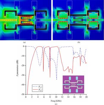
Figure 6(a, b) depicts the current distribution in the proposed UWB filter at the dual notch frequencies from which it can be observed that for 5.8 GHz, the maximum current is concentrated around the SDGS, whereas for 8 GHz, the SRRs show increased current density concentration on them. These localized current densities around the SDGS and on the SRRs emphasize their pronounced effect on creating the respective notches compared with rest of the UWB parameters. The optimized frequency characteristics of the dual notched band UWB filter is plotted in Fig. 6(c). The optimized dimensions of the dual notched band UWB-BPF are mentioned in Table 2. The proposed structure is compared with other structures in Table 3.
Transmission phase characteristics of the UWB filter with and without SDGS units (all four SRRS units absent).

(a) Current distribution in the UWB filter at 5.8 GHz. (b) Current distribution in the UWB filter at 8 GHz. (c) Optimized simulated response of the dual notched band UWB filter.

Optimized dimensions of the dual notched band UWB-BPF

Comparison of our proposed structure with other recently reported dual notched band UWB-BPF

It can be observed from Table 3, that the proposed structure meets the necessary UWB passband requirement with appreciable attenuation at the dual notch positions. The stopband is wide and deeper than 20 dB, thereby providing sufficient isolation. Also, the biggest feature of the proposed structure is its very compact size compared with the rest [Reference Wu and Chen2–Reference Song, Yang and Geyi13].
Experimental verification
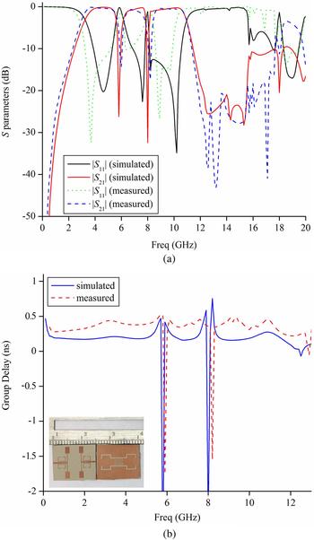
In order to validate the data obtained through simulation, we developed an experimental prototype of the proposed structure and measured its frequency characteristics using Agilent Vector Network Analyzer N5230A. The measured data are compared with the simulated results in Fig. 7(a, b), from which deviation between the two is observed. This may be attributed to finite substrate size, unexpected fabrication tolerances, connector reflections, etc. Figure 7(a) depicts passband width from 3 to 10.9 GHz with dual notches centered at 5.96 and 8.15 GHz, respectively, and an extended stopband till 16 GHz possessing attenuation > 20 dB. The passband insertion/return loss is better than 0.6 dB/15 dB between the lower cut-off frequency and the first notch (3–5.7 GHz), 0.86 dB/11 dB between the first and second notch (6.25–7.76 GHz), and 0.48 dB/17 dB after the second notch till the upper cut-off frequency (8.451–10.9 GHz). The measured group delay, plotted in Fig. 7(b), shows variation between 0.47 and 0.18 ns (except at notches), thereby displaying appreciable linearity. The proposed filter covers a total circuit area of only 14.6 × 7.3 mm2.
(a) Comparative S parameters characteristics of the simulated and measured response. (b) Comparative measured and simulated group delay.

Conclusion
This paper presents a compact UWB filter with dual notches at 5.8 and 8 GHz. The hybrid microstrip/CPW transition technology is utilized to develop the basic UWB filter, wherein a short-circuited SIR is present within a CPW in the ground and is vertically coupled to two microstrip lines on the top. The optimized coupling of this alignment develops a four pole UWB-BPF with good insertion/return loss. The dual passband notches and extended stopband are implemented using the transmission zeros of SDGS (etched in SIR in the ground plane) and four SRRs (coupled to I/O lines) on top. The S parameters and group delay of the experimental prototype exhibits appreciable agreement with the simulated data. These pleasing frequency characteristics combined with its miniaturized size makes the proposed structure a necessary additive to any UWB communication system.
Acknowledgements
The authors appreciate Sunrays Circuits, Bangalore, for their generous help in filter's fabrication.
 Abu Nasar Ghazali received his B.Tech. degree in Electronics & Communication Engineering (ECE) from SRM University, Chennai, in 2008 and M.E. degree in Microwave Engineering from Birla Institute of Technology (BIT) Mesra, in 2010 where he was a GATE scholar. He completed his doctorate in 2014 from BIT Mesra. He worked as an Assistant Professor (I) in the Department of ECE at the BIT Mesra, Patna campus. Currently, he is an Assistant Professor (II) in the School of Electronics Engineering, at the Kalinga Institute of Industrial Technology (KiiT), Bhubaneswar, India. He is an Associate member, The Institution of Engineers (IEI), India and member of IEEE. He has published quite a few papers in SCI/SCOPUS indexed journals and conferences. His main research interests are UWB filters, Microstrip filters, and passive microwave circuit components.
 Mohd Sazid received his B.Tech. degree in ECE from Uttar Pradesh Technical University in 2011 and M.E. degree in Wireless Communication Engineering from BIT Mesra in 2015 where he was a GATE scholar. He is currently working as an Assistant Professor in the Department of ECE at the Noida Institute of Engineering & Technology. He has published several papers in SCI indexed journals. His main research interests are UWB filters and microstrip-based passive circuit components.
 Srikanta Pal received his B.Tech. degree in Electronics & Communication Engineering from NIT Warangal, India and M.Tech. degree in Microwave Engineering from Jadavpur University, Kolkata, India in 1990 and 1992, respectively. From 1992 to 2000 he was with the R&D Antenna Lab of the Bharat Electronics Limited (BEL). In 2001, he joined the Oxford University as a Research Associate where he worked toward his Ph.D. on HTS Microwave Filters, which he completed in 2003. From 2003 to 2005 he was a visiting Faculty in the Centre for Advanced Research in Electronics (CARE) Department at the IIT Delhi, India. In 2005, he joined the Department of Electronics and Computer Engineering at the IIT Roorkee, India, as an Assistant Professor. He joined the Emerging Devices Technology Center at the Birmingham University as a Post Doctorate fellow in 2006 where he designed a HTS filter which is currently installed in the world's largest Telescope, Green Bank Telescope (GBT), West Virginia, USA. In 2008, he joined the ECE Department at the BIT Mesra where he is currently working as a Professor and Head of the Department. He is also a lifetime Research Fellow at the University of Birmingham. His research interests include RF Filters and Devices, MEMS, HTS Microwave filters, Antennas and Computational Electromagnetics.