I. INTRODUCTION
Radio frequency (RF) feed networks are essential in any multi-antenna or multi-line microwave system. Such networks are used in antenna arrays to perform beamforming (BF) and null steering (NS). The control of the beams/nulls is achieved by changing the relative amplitudes or phases or both between different antenna elements. RF beamformers are either networks or quasi-optical lenses. The main difference between them is that the beam angles are fixed (independent) with frequency changes in lenses, while they change with frequency in network-based beamformers. From this fact, lenses are considered wide-band while networks are narrow-band. The Butler matrix is an example of a network beamformer, whereas the Rotman lens is a quasi-optic one. These two are the most popular ones and have many practical applications.
The Butler matrix [Reference Butler and Howe1] consists of hybrid couplers, phase shifters, and crossovers. It has a simple structure for small number of beams. However, since it has crossovers, a multilayer structure is required for large number of beams (larger number of inputs/outputs). The beam ports are usually isolated and the number of beams are typically a power of two. A four-beam Butler matrix feeding a four-square monopole array was presented in [Reference Solbach and Angenendt2] and covered a range of frequencies from 2.4 to 3.4 GHz. Another matrix fabricated using MMIC technology was developed in [Reference Chang, Chin, Wu and Chang3]. It was packaged on a chip of size 1.36 × 1.47 mm2 that works only at 2.4 GHz.
In [Reference Chang, Lee and Shih4], a combination of a conventional Butler matrix and tunable phase shifters was introduced to improve the beam resolution. The tunable phase shifters were responsible only for steering the beam in the range between two adjacent beams that were created using a Butler matrix. The overall circuit size was 175 × 135 mm2 with a full scanning range of 108° It operated between 1.6 and 2.8 GHz. An approach based on vector modulation to achieve controlled phase shifting for BF applications was presented in [Reference Hutu, Cordeau and Paillot5]. This technique is performed on the I/Q components of the signal and suffers from high complexity. It also operated within limited frequency bands. While in [Reference Yu and Rebiez6] a compact six-bit programmable phased array front end was proposed but for frequencies covering 24 GHz.
A Rotman lens [Reference Rotman and Franchi7] is a true time-delay beamformer and hence the beam angles are independent of frequency. It has complex design parameters. The Rotman lens can provide low sidelobes (as low as −33 dB) [Reference Thomas8]. A 2.4 GHz Rotman lens was designed in [Reference Lin and Liao9] for multiple-input and multiple-output (MIMO) applications. It provided a four-beam lens and generated four scanning beams. Its frequency of operation was 2.4 GHz and occupied a size of 19.3 × 22.3 cm2 An 8 × 8 Rotman lens was developed in [Reference Rahimian and Rahimian10] to be used in vehicle-to-vehicle communications systems. It occupied a size of 359.1 × 258 mm2 and operated at 3.15 GHz.
As noticed from the previous work, network beamformers have easy structures for small number of beams. But for a large number of beams, the design will be very complicated especially for crossovers and the directional couplers that need multilayer structures. Also, most of them are valid only for narrow band applications. Network beamformers can only provide a certain number of beams that are pre-defined and cannot be changed. So, it is difficult to reprogram them to cover other angles. The side-lobes in such networks are relatively high because they do not have amplitude control capability. Lens-based beamformers provide wider frequency coverage but with larger dimensions. They have good isolation between their ports. It is difficult to achieve linear progressive phase with lenses due to their complicated curvature structure. Finally, all of the programmable feed networks for antenna array applications were realized at very high frequencies (i.e. higher than 10 GHz).
To come up with a wideband feed network that is digitally programmable with high resolution in amplitude and phase as well as compact in size is a relatively challenging task. In this work, we propose a digitally controlled programmable wideband RF feed network that covers the frequency band from 2.5 to 6 GHz. A complete path of the network occupies 70 × 51 mm2 and two paths occupy 111 × 63 mm2 (i.e. to feed two antennas). The design architecture will be explained in Section II. The fabricated design followed by the measured results are described in Section III. Conclusions are stated in Section IV.
II. DESIGN ARCHITECTURE
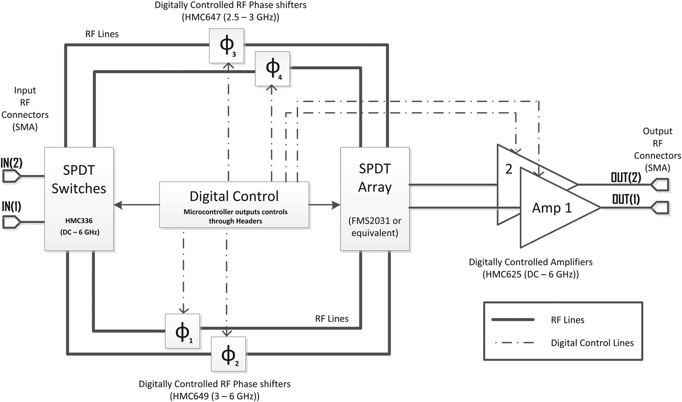
As shown in Fig. 1, the design architecture of the proposed two-path feed network is composed of four main stages; RF switching, phase shifting, amplification, as well as the digital control. The wideband coverage is achieved through two separate branches, one covered the frequency range from 2.5 to 3 GHz and the other covered 3–6 GHz. Two switching stages were used at the input and output sides of the phase shifters. A broadband GaAs MMIC single-pole double-through (SPDT) non-reflective switch was used. The switch covered the range from DC-6 GHz and high isolation (42 dB at 6 GHz) and low insertion loss (1.6 dB at 6 GHz). The switching time was typically 20 ns. GaAs MMIC six-bit digitally controlled phase shifters that provide 360° of phase coverage with phase resolution of 5.625° were used. The first one (HMC647) covered the lower frequency range (2.5–3 GHz) and the second-phase shifter (HMC649) covered the higher frequency range from 3 to 6 GHz. Once the phase shift is imposed on the incoming signal, a GaAs MMIC six-bit digitally controlled variable gain amplifier is used for amplitude control. The amplifier covers the range from DC to 6 GHz and can be programmed to provide anywhere from −13.5 to 18 dB of gain in 0.5 dB increments. The amplifier does not have a flat gain versus frequency response. It has a maximum gain of 18 dB that decreases to about 5 dB at 6 GHz. The amplifier has two modes of operation, serial and parallel. The parallel mode was used to guarantee the fastest response for the amplifier (12 ns response time compared to 0.8 µs for the serial mode). The chosen components were picked based on their size and resolution since high resolution as well as compact size were of the design requirements.
Design architecture of the proposed programmable feed network.

III. RESULTS AND DISCUSSIONS
The fabricated board is shown in Fig. 2. It consists of two paths that can feed two antennas. Since we have two phase shifters in each path to cover the whole range, each path has two branches. The paths are identical and occupy very small area to minimize the board size. The dip-switches consume most of the board size because each main component (phase shifter and amplifier) has a separate dip-switch that cannot be shared. These switches can be replaced by headers or a main digital control unit such as a Microcontroller to reduce the size and integrate the proposed feed network in a system level solution.
Fabricated board of the proposed two-path network (to feed two antennas).
The board was built on an FR-4 substrate material with 0.8 mm thickness and relative permittivity (ε r) of 4. The total size of the two-path feed network was 111 × 63 mm2. Measurements were conducted using an Agilent N9918A vector network analyzer (VNA). The phase changes with typical steps of 5.6° are shown in Fig. 3. Measured and simulated results were in very good agreement. The maximum measured step was 6.7° and the minimum one was 4.6° with an error of +1°. The proposed network provides this step resolution over the whole frequency band, from 2.5 to 3 GHz in Fig. 3, and from 3 to 6 GHz as shown in Fig. 4. For a linear array feed, a scanning beam of resolution 1.8° can be achieved using these steps. This provides finer resolution and more flexibility compared to that obtained from [Reference Chang, Lee and Shih4] at the expense of using extra electronics (the microcontroller unit). In addition, the complexity of the proposed design is much lower than that of [Reference Hutu, Cordeau and Paillot5].
Measured phase results with 5.6° step (2.5–3 GHz).
Measured phase results (7 curves.) covering 0–33.75° in 5.6° steps (3–6 GHz).
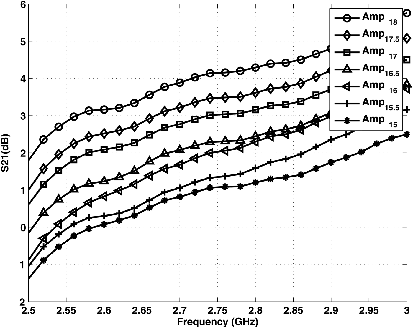
Figures 5 and 6 show the amplitude changes with a resolution of about 0.5 dB per step, with a maximum error of 0.22 dB in the two bands, respectively. The amplifier has a maximum gain of 18 dB and goes down to −13.5 in 0.5 dB increments and 64 steps (six-bit control). The maximum achieved gain in the 2.5−3 GHz was 5.5 dB due to the combined insertion loss from the other components (typical losses of 11 dB without RF lines and bends). A linear phase response was obtained. Thus, the phase resolution from the phase shifters will not be affected by the amplifier amplitude changes. Figure 7 shows the phase response of the design for different amplitude steps. A phase stability of <+ 1° is achieved over a wide range of amplitudes. In addition, amplitude stability is achieved. Figure 8 shows how the amplitude does not change with different phase steps. The amplitude error was <0.15 dB.
Measured amplitude results with 0.5 dB steps (2.5–3 GHz).
Measured amplitude results with 0.5 dB step (3–6 GHz).
Phase response for amplitude changes.
Amplitude response for different phase changes (18 dB gain step).
IV. CONCLUSION
A wideband digitally programmable RF feed network operating in the range form 2.5 to 6 GHz was designed and fabricated. The fabricated board had a total size of 111 × 63 × 0.8 mm3 and was fabricated on a commercial FR-4 substrate. This is a standalone design that can be applied to any type of antenna array or multi-path RF system. The results showed measured amplitude resolution of 0.5 with 0.22 dB maximum deviation and phase resolutions of 5.6° with 1° maximum deviation.
ACKNOWLEDGEMENTS
This work was supported by the Deanship of Scientific Research (DSR) at King Fahd University of Petroleum and Minerals (KFUPM), Saudi Arabia, under project number FT111001.
 Mohammad S. Sharawi is an Associate Professor of Electrical Engineering at King Fahd University of Petroleum and Minerals (KFUPM), Dhahran, Saudi Arabia. Dr. Sharawi is the Founder and Director of the Antennas and Microwave Structure Design Laboratory (AMSDL). He was a Research Scientist with the Applied Electromagnetics and Wireless Laboratory in the Electrical and Computer Engineering Department, Oakland University, Michigan, USA, during 2008–2009, and a visiting research professor in the summer of 2013. He obtained his Ph.D. in RF Systems Engineering from Oakland University, Michigan, USA, in 2006. During 2002–2003 he was a hardware design engineer with Silicon Graphics Inc., California, USA. Dr. Sharawi has more than 90 refereed International Journal and Conference paper publications. His research interests include Printed and MIMO Antenna design and characterization, RF electronics, and Applied Electromagnetics. He has two issued and nine pending patents.
 Sameir E. Deif received his B.Sc. degree in Electronics and Communication Engineering from Mansoura University in Mansoura, Egypt in 2007. He obtained his M.Sc. degree in Electrical Engineering, specialized in RF/microwave circuits from King Fahd University of Petroleum and Minerals, Dhahran, Saudi Arabia in 2013. His main research interests are in printed antenna designs and RF circuits. He is currently employed as Technical Research Assistant, Deanship of Research, at King Fahd University of Petroleum and Minerals.
 Elias Ghafari received his B. Eng. and M.S.E.E. degrees in Electrical Engineering specialized in Antennas and Microwaves Circuits from Concordia University in Montreal, Quebec, Canada in 1996 and 2006, respectively. He obtained his Ph.D. degree in Electrical Engineering, specialized in antennas from Oakland University in Rochester Hills, Michigan, USA in 2013. His main research interests are in printed antenna designs and RF circuits. He has over 18 years of design experience in antennas and RF/microwave circuits for a broad spectrum of applications and markets. He is currently employed as a senior antenna Design Engineer at Blaupunkt Antenna Systems.
 Daniel N. Aloi is a Professor and Chair in the Electrical and Computer Engineering Department at Oakland University, Rochester, Michigan. He received his B.S. (1992), M.S. (1996) and Ph.D. (1999) degrees in Electrical Engineering from Ohio University, Athens, Ohio. His research interests resided in the area of Applied Electromagnetic with emphasis on antenna measurement/design for the automotive and aviation industries. He was awarded the National Science Foundations 2005 Major Research Instrumentation award to construct an on-campus, outdoor vehicle level spherical near-field antenna measurement facility that operates in the frequency range extending from 50 MHz to 6 GHz. Professor Aloi has served as a PI on external grants and contracts in excess of $3 M dollars from private industry, NSF, FAA, and DARPA. In addition, he has authored over 70 technical papers and is an inventor on six patents. He currently serves as the technical editor in the area of navigation for the IEEE Transactions on Aerospace and Electronic Systems.