I. INTRODUCTION
Organic materials with defined electronic properties have received considerable attention during the last decades. When coupled with low-cost fabrication techniques, they are expected to receive an enormous upswing in different market fields such as light-weight large screen displays, low-end electronic devices, including smart cards, electronic paper, cheap identification tags, and large-area sensing applications.Reference Loo and McCulloch1 In advanced organic electronic circuits, as are used for radio frequency identification tag (RFID) transponder chips and system-in-foil technologies,Reference Myny, Steudel, Smout, Vicca, Furthner, van der Putten, Tripathi, Gelinck, Genoe, Dehaene and Heremans2–Reference Sekitani, Takamiya, Noguchi, Nakano, Kato, Sakurai and Someya4 it would be highly desirable to have a much faster complementary logic than is state-of-the-art.
The basic element of digital logic, the inverter, is composed of two organic thin film transistors and acts as a logic NOT gate. For being effectively used in integrated circuits, organic inverters require high gain, low operation voltage, absence of hysteresis, and high switching speed.Reference Sekitani, Takamiya, Noguchi, Nakano, Kato, Sakurai and Someya4–Reference Gundlach, Pernstich, Wilckens, Gruter, Haas and Batlogg6 The operating frequency of the inverter is limited by the channel transit time of the charge carriers and the charging and discharging times of the gate capacitance.Reference Klauk, Gundlach and Jackson7 Since the source-to-drain transit time is proportional to the square of the effective channel length of the individual transistors, downscaling of the critical device dimensions is very important to increase the operation frequency.
For common commercially available organic semiconductor materials with a charge carrier mobility around 0.1 cm2/Vs, a reduction of the channel length to scales below 1 μm and an adequate downscaling of the gate dielectric layer thickness are necessary to reach the MHz regime of circuit operation. Solutions along these lines have already been demonstrated for p-type semiconductors.Reference Haas, Gold, Haase, Jakopic and Stadlober8–Reference Auner, Palfinger, Gold, Kraxner, Haase, Haber, Sezen, Grogger, Jakopic, Krenn, Leising and Stadlober10
An important issue in complementary organic inverters is the right choice of material combinations. Pentacene is very popular for the p-type semiconductor but needs an n-type material with sufficiently high mobility to be complemented adequately. Copper hexadecafluorophthalocyanine (F16CuPc) is known to be a relatively stable n-type semiconductor achieving field effect mobilities in the range of 10−2 cm2/Vs.Reference Vusser, Steudel, Myny, Genoe and Heremans11, Reference Bao, Lovinger and Brown12 Its lowest unoccupied molecular orbital (4.8 eV) is close to the work function of Au (5.0 eV).Reference Shen and Kahn13 With regard to an implementation of the n-type device within a complementary circuit with pentacene as the p-type material, the possibility of using gold electrodes for both, the p- and the n-type device, is a decisive fabrication issue. The combination of F16CuPc and pentacene for the production of organic complementary inverters and small logic circuits was reported by several groups,Reference Vusser, Steudel, Myny, Genoe and Heremans11, Reference Crone, Dodapalapur, Lin, Filas, Bao, LaDuca, Sarpeshkar and Katz14, Reference Klauk, Zschieschang, Pflaum and Halik15 whereas Gundlach et al.Reference Gundlach, Pernstich, Wilckens, Gruter, Haas and Batlogg6 demonstrated the combination of PTCDI-C13H27 (N,N’-ditridecylperylene-3,4,9,10-tetracarboxylic diimide) and pentacene in complementary inverters first. Because these inverters needed very high supply voltages (up to 100 V) which are incompatible with most specifications in organic electronic applications, Tatemichi et al.Reference Tatemichi, Ichikawa, Kato, Koyama and Taniguchi16 presented a promising low-voltage approach with the high-k Ta2O5 as gate dielectric on the same semiconductor material base.
The main target of this work is the fabrication of flexible complementary organic transistors and inverters with a low-voltage onset. In view of large-area structuring, high integration level, and high operation frequencies, we combine the organic complementary transistor approach with submicron channel transistors patterned by nanoimprint lithography (NIL). Within the scope of this work, two different approaches for device fabrication were followed. One uses a standard SM technique, a very thin nanocomposite material (ZrO2+pαMS) as a high-k dielectric layer,Reference Zirkl, Haase, Fian, Schön, Sommer, Jakopic, Leising, Stadlober, Graz, Gaar, Schwödiauer, Bauer-Gogonea and Bauer17 and the semiconductor combinations pentacene/PTCDI-C13H27 as well as pentacene/F16CuPc. The second approach addresses downscaling, device integration, and higher circuit speeds and is based on high-resolution patterning by NIL. Here an organic dielectric from a liquid precursor, a benzocyclobutene (BCB)-derivative,Reference Chua, Ho, Sirringhaus and Friend18 was chosen, and the n-type semiconductor was F16CuPc.
II. EXPERIMENTAL
A. Nanoimprint lithography
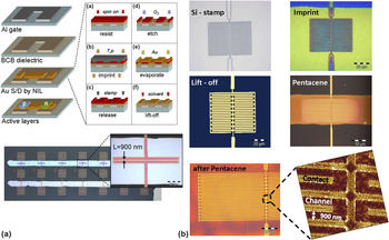
A scheme of the NIL process is shown in Fig. 1. On 60 nm of aluminium as gate electrode (patterned by photolithography), a 100-nm-thick layer of BCB (Cyclotene by Dow Chemicals, Midland, MI) is fabricated by spin coating a solution of 1:3 BCB in 1,3,5-trimethylbenzene (Mesitylene) at 2000 rpm for 30 s. On a hotplate, the layer is cross-linked at 290 °C for 60 s. Alternatively, a nanocomposite ZrO2/Poly(vinyl cinnamate) (PVCI) is built by reactive sputtering of Zr in an oxygen gas atmosphere.Reference Zirkl, Haase, Fian, Schön, Sommer, Jakopic, Leising, Stadlober, Graz, Gaar, Schwödiauer, Bauer-Gogonea and Bauer17 Starting with a vacuum of 10−7 mbar, Argon (sputtering gas) and oxygen (reaction gas) are streamed into the chamber (ratio 5:2), until a pressure of 6 × 10⁻³ mbar is reached. A ZrO2 layer of 40 nm thickness is formed at a rate of 6 Å/min. A thin layer of PVCI is applied by spin coating at 2000 rpm for 30 s. The layer is cross-linked by UV illumination with a wave length of 254 nm for 1 h. As a further alternative for the gate dielectric, a 140-nm thin layer of an organic–inorganic hybrid material (Ormocer, Würzburg, Germany) was tested. It is baked at 150 °C and cross-linked by UV light. This material has already been shown to be a high-quality gate dielectric in micron- and submicron-sized p-type and n-type organic thin-film transistors (OTFTs).Reference Haas, Haase, Satzinger, Pichler, Leising, Jakopic, Stadlober, Houbertz, Domann and Schmitt19–Reference Palfinger, Auner, Gold, Haase, Kraxner, Haber, Sezen, Grogger, Domann, Jakopic, Krenn and Stadlober21 The dielectric layer has to meet a range of requirements to survive the subsequent nanoimprinting process, most of all it must be stable against standard organic solvents and a short oxygen plasma treatment. The thermal imprint resist mr-I7030E (micro resist technology GmbH, Berlin, Germany) is spin-coated onto the dielectric surface and dried on a hotplate for 3 min at 140 °C. The stamp (silicon, patterned by e-beam lithography and anisotropic dry etching, coated with perfluoroctyl-trichlorosilane for antiadhesion) containing the source and drain patterns is aligned to the gate electrode (done in an EVG 620 mask aligner, EV Group, Schärding, Austria), and the stamp sample system is transferred to the hot embossing tool (EVG 520 hot embosser EV Group, Schärding, Austria). The resist is heated up well above its glass transition temperature T g = 80 °C, the stamp is pressed into the resist and the whole stack is cooled down again. After releasing the stamp, the source/drain patterns have been transferred to the sample with a thin residual layer left, which has to be removed by a short anisotropic oxygen plasma etch. A 35-nm-thick gold layer is thermally evaporated onto the sample. Nonimprinted regions of the resist are lifted off in a PGMEA (1-methoxy-2-propylacetate) bath and leave the source/drain electrodes on the sample. Patterned by SM, both small molecule semiconductor materials are successively evaporated onto the sample. The pentacene layer is fabricated in high vacuum (10−6 mbar) with the substrate held at 65 °C and rotated with 8 rpm. The deposition rate is slowly increased during the process from 1 Å/min for the first 5 nm to finally 5 Å/min, until a layer thickness of 30 nm is reached. This stepwise increase of the deposition rate results in polycrystalline pentacene growth with low nucleation density, and therefore, leads to good device performance at a reasonable processing time. For the n-type organic semiconductor (OSC) a 30-nm-thick layer of F16CuPc is used, applied at a substrate temperature of 90 °C.
(a) Process scheme and micrograph of organic inverters fabricated by NIL, (b) micrographs of a nanoimprint lithography (NIL) structure showing the stamp, the imprint, the liftoff, and pentacene evaporation, as well as an atomic force microscopic image of the transistor.

Both imprinted transistors have a channel length of L = 900 nm, while their widths were adapted for mobility compensation, being W p = 10 μm and W n = 100 μm. The substrate is a polyimide (Kapton) foil, showing high resistance to the necessary temperatures for BCB crosslinking.
B. SM patterning
For the gate electrode, 80 nm of aluminium are e-beam evaporated on a precleaned glass substrate at a rate of 0.3 nm/s. During the evaporation, the substrate is rotated at 8 rpm to ensure a homogeneous thickness of the Al layer. The dielectric material is a double-layer nanocomposite material consisting of ZrO2 and poly(α-methylstyrene). The ZrO2 layer is built as stated in the NIL section. Afterward, a thin polymer film (PαMS) is applied on top of the metal oxide. It acts as a smoothing layer, filling up the small voids occurring between the ZrO2 islands. This significantly reduces leakage currents and allows for low operation voltages.Reference Fian, Haase, Stadlober, Jakopic, Matsko, Grogger and Leising22, Reference Jang, Kim, Nam, Chung, Yang, Yun, Park and Koo23 A solution of 0.5 wt% of PαMS (MW 300.000) in toluene was spin coated at 4000 rpm for 30 s and baked for 15 min at 150 °C on a hotplate. The semiconductors are thermally evaporated one after the other. The pentacene as well as the F16CuPc layers are fabricated as described in the NIL section. The n-type OSC PTCDI-C13H27 is grown heating the substrate to 40 °C, again under high vacuum conditions. During the evaporation process, the rate was increased from 2 for the first 10 nm to 4 Å/min for the remaining 25 nm.
The top electrodes are made from an 80-nm-thick gold layer, applied by e-beam evaporation at a rate of 0.3 nm/s. No substrate rotation was applied to assure highly defined patterning through the SM. Particle scattering at shadow mask edges or insufficient mechanical contact (between mask and substrate) can cause inaccurate pattern transfer. For better comparison with the NIL inverters, we used the same channel width ratio (W p/W n = 1:10), with W p = 1 mm and W n = 10 mm while keeping the channel length of both transistors at L = 100 μm.
III. RESULTS AND DISCUSSION
A. SM-patterned OTFTs
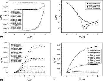
OTFTs fabricated by SM techniques were built as a reference for the NIL devices. Figure 2 shows their output characteristics I DS(V DS) with I DS being the drain current and V DS the drain voltage. The pentacene p-type transistor has an on/off ratio of I on/off = 104 at −3 V drain (V DS) and gate (V GS) voltage [Fig. 2(a)]. The threshold voltage is V T = −2.1 V and the maximum mobility amounts to μ = 0.5 cm2/Vs. The n-type device fabricated with an active layer of PTCDI shows an on/off ratio of I on/off =104, a maximum mobility μ = 4 × 10⁻² cm2/Vs and a threshold voltage of V T = 1.6 V. The device shows clear signs of contact resistances [curved linear regime, see Fig. 2(b)], a further indication of an electron injection barrier in combination with gold electrodes. Saturation is very good, which is necessary for good inverter behavior. Using F16CuPc as an alternative n-type semiconductor, the transistor delivers I on/off = 103, μ = 5 × 10⁻³ cm2/Vs, and V T = 0.8 V. The electronic levels seem to fit better to the work function of gold, as no curvature of the linear regime is observed [Fig. 2(c)]. In general, the mobility values of the n-type devices are at least a factor of ten smaller than the ones of the p-type OTFTs.
(a) Pentacene shadow-mask patterned (SM) transistor output I DS(V DS) and transfer I DS(V GS) characteristics, maximum gate leakage current I Gmax = −7 × 10⁻¹⁰ A (b) Output characteristics of a PTCDI SM transistor, I Gmax = 4.5 × 10⁻⁹ A, and (c) a F16CuPc SM transistor, I Gmax = 9 × 10⁻⁹ A.

B. Nanoimprint lithography OTFTs
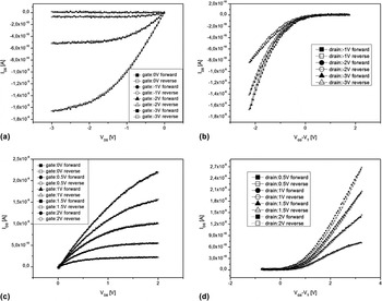
To address industry-related topics such as higher switching speeds, downscaling, and integration, we fabricate our devices by using a hot embossing or thermal NIL process.Reference Haas, Gold, Haase, Jakopic and Stadlober8 As a first step, we evaluated different dielectrics, namely a BCB-derivative, ZrO2/PVCI,Reference Zirkl, Haase, Fian, Schön, Sommer, Jakopic, Leising, Stadlober, Graz, Gaar, Schwödiauer, Bauer-Gogonea and Bauer17 and a hybrid material from the class of Ormocers. We built p-type transistors with a channel length of 900 nm and an active layer of pentacene. All devices show low-voltage operation, good saturation, and a mobility in the range of 10−3 cm2/Vs (BCB: μ = 2.6 × 10⁻³ cm2/Vs, ZrO2/PVCI: μ = 2 × 10⁻³ cm2/Vs, Ormocer: μ = 4 × 10⁻³ cm2/Vs). The transistor widths are 10 μm for BCB and Ormocer, the ZrO2 device has a width of 100 μm. These results demonstrate that all gate dielectrics are suitable for further usage in our research toward downscaled integrated circuits. We opted to use BCB due to its easy and fast processing. Accordingly, all NIL transistor and inverter characteristics shown in this work are fabricated using a BCB dielectric. In Figs. 3(a) and 3(b), the characteristics of a p-type submicron OTFT with a threshold voltage of V T = 0.75 V are illustrated.
Output I DS(V DS) and transfer characteristics I DS(V GS,eff) of flexible NIL transistors with (a, b) pentacene and (c, d) F16CuPc as active layers—Gate leakage currents are I Gmax = 1 × 10⁻¹⁰ A and IGmax = 3.4 × 10⁻¹⁰ A, respectively.

The n-type transistors are fabricated with a ten times larger channel width than the p-type devices. According to complementary metal oxide semi-conductor (CMOS) inverter theory, it is important that the drain currents of both transistors are equal.Reference Rabaey, Chandrakasan and Nikolic24 Changing the transistor geometries should compensate for the expected lower mobility of the n-type semiconductors. According to the results of the SM devices, we expected a mobility difference of at least one order of magnitude and changed the n-type transistor width to 100 μm.
For the fabrication of n-type transistors, the organic semiconductor PTCDI with its high mobility would be preferable, but despite our best efforts we were not able to fabricate working devices. To our best knowledge, only Hong et al.Reference Hong, Kim, Yang, An, Cha, Park and Park25, Reference Hong, Kim, Yang, Jang, Cha and Park26 reported working bottom contact OTFTs with gold source/drain electrodes. The devices reveal very low mobility due to a high electron injection barrier, improved results were achieved using PEDOT:Tos electrodes instead. Using different electrodes for the p-type and n-type devices did not seem convenient concerning the later fabrication of complementary circuits, thus we opted to switch to a different semiconductor material.
For F16CuPc as an active layer, the transistor reveals the characteristics shown in Figs. 3(c) and 3(d). The mobility adds up to μ = 2.3 × 10⁻⁴ cm2/Vs, the threshold voltage is V T = −1.25 V, making the device normally on. Full saturation of the drain current can be expected for V DS > V GS,eff = V GS−V T ∼ V GS + 1.25 V; accordingly saturation in the I DS(V DS) graph is only visible for the curves with gate bias below 1V [Fig. 3(c)].
In general it can be stated, that the mobility level of the NIL devices is lower than that one of the SM devices because of a number of reasons. These can be mostly attributed to the bottom S/D geometry resulting in a higher contact resistance and a worse morphology of the semiconductors due to process-induced degradation of the dielectric interface quality.
A comparison of the transfer characteristics between p- and n-type transistors is best applicable, if the curves are plotted against the effective gate voltage (V GS,eff = V GS−VT) [Figs. 3(b) and 3(d)]. For identical gate dielectric capacitance values this enables to directly compare the charge carrier mobility via the drain current level irrespective of the threshold voltage. It turns out that almost the same drain current level │I DS│ is achieved for │V DS│=│V GS,eff│, thus justifying the width ratio of 10:1 between n- and p-type NIL transistors which was chosen from the SM results to account for the mobility difference. However, since the p- and especially the n-type NIL devices are normally on, displaying threshold voltages that are asymmetric with respect to 0 V a perfect match of the drain current levels could not be achieved in this first design cycle. From this it is deduced that in the next design cycle a width ratio of 2:1 between n- and p-type OTFTs has to be chosen which better accounts for the strong V T asymmetry.
In comparison with the SM devices, both the nanoimprinted p- and n-type transistors have a mobility that is about one order of magnitude smaller. The F16CuPc devices also show a negative shift of V T, changing their behavior from normally off (SM) to normally on (NIL). One explanation could be the presence of trapped positive charges at the interface in NIL devices that induces the attraction of mobile electrons thus making the n-type transistor normally on. The increase of the interface trap density in lithographically fabricated devices is also reflected in an increase of the subthreshold swing from values around 100mV/dec in SM patterned devices [see Fig. 2(a)] to more than 500 mV/dec in imprinted devices.
C. SM inverters
Symmetric drain currents are needed for symmetric inverter behavior, resulting in the need for an adaption of the channel width to compensate for the one order of magnitude lower mobility of n-type semiconductors.
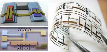
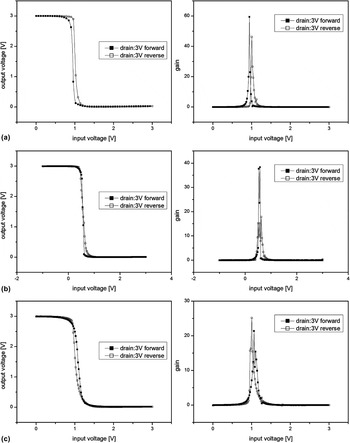
A schematic inverter architecture, a micrograph of a single complementary inverter and respective photos are displayed in Fig. 4. The transfer characteristics of three different inverters are shown in Fig. 5. The first inverter is based on pentacene and PTCDI for the active layers [Fig. 5(a)]. At a supply voltage of Vdd = 3 V, the realized high level is V OH = 3 V. The low level of V OL = 30 mV is a bit higher than the theoretical achievable 0 V. The reason for this is the off-current of the p-type transistor being one order of magnitude higher than that of the n-type transistor. The gain reaches the excellent value of 55. The inverter is not perfectly symmetric, being caused (i) by a slight mismatching of the charge carrier mobilities of the single transistors apart from the targeted 1:10 ratio and (ii) by a threshold voltage difference of the single transistors of around Δ|Vth| = 0.5 V. The inverter’s threshold voltage is V ti = 0.97 V. Overall the results look very promising, the inverter can be clearly used in logic gate circuits. Although symmetry is not completely given, still both, the high and the low level, are in the positive regime and well within the input voltage range of 0–3 V. The noise margin is reasonably large (∼0.9 V), mainly limited by the asymmetry of the threshold in the inverter transition curve.
SM Inverter: Scheme of the SM inverter architecture, micrograph of a single inverter fabricated on glass, and photograph of a sample with flexible inverters on a PET substrate.

Transfer characteristics and gain of SM inverters on (a) a glass substrate using pentacene/PTCDI as active layers, (b) on PET foil using pentacene/PTCDI, and (c) on PET foil using pentacene/F16CuPc.

As a next step precleaned Polyethylene terephthalat (PET) foil with a thickness of 175 μm was used as a substrate. Figure 5(b) shows the electrical characteristics of the flexible device. Comparable to the results on a glass substrate (Fig. 4), a supply voltage of V dd = 3 V lead to a high level of V OH = 3 V, while the low level reached V OL = 6 mV. Again the gain is quite high, reaching values of about 40. The inverter threshold voltage is V ti = 0.55 V. The device shows clearly, that flexible substrates can be used in the process, which is important for future large-area fabrication.
To improve comparability with the NIL inverters, we also fabricated devices with F16CuPc as n-type material [Fig. 5(c)]. The high and low levels are equal to the results using PTCDI, revealing V OH = 3V and V OL = 20 mV. The gain is lower, reaching a value of 20 and the inverter threshold voltage is V ti = 1.04 V. The lower gain can most likely be attributed to the weaker saturation of the F16CuPc compared to PTCDI transistors at the chosen supply voltage of 3 V.
D. NIL inverters
As stated earlier equal drain currents flowing through both transistors are needed for an inverter with a threshold at V DD/2. Increasing the channel width of the F16CuPc OTFT to compensate for the one order of magnitude lower mobility seemed reasonable and worked well for the SM devices. However, the shift of V T toward the normally on regime in imprinted F16CuPc devices results in a higher drain current. Comparing the p- and n-type transistors at V GS = V DS = 2V, the drain currents are I Dp = 4 × 10⁻¹⁰ A and I Dn = 2 × 10⁻⁹ A, respectively (see Fig. 3). The early onset of the F16CuPc device already compensates for the lower mobility, it would not be necessary to change the transistor geometries. However, the strength of the V T shift was not expected when designing the inverters and the ratio of the transistor widths remained W p/W n = 1/10.
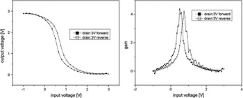
The resulting imprinted complementary inverter with submicron transistor channels displays an inverter characteristic (Fig. 6) with a low level of V 0L = 25 mV at V I = 3 V, which is comparable to the shadow mask patterned devices (Figs. 4 and 5). The high level of V 0H = 2.9 V is only reached at negative input voltages of V I = −1 V. The reason for this is, as stated above, the threshold voltage of the n-type transistor, which is V T = −1.25 V, making the device normally on. The rather low gain of 4.2 can also be attributed to the n-type transistor performance, where saturation in the output characteristics is not reached within the inverter operation voltage range. To improve the inverter performance, further studies especially concerning the n-type transistor, are required and will be performed. Also future designs will take the threshold voltage of the n-type transistors into account. To the best of our knowledge, this is the first demonstration of a flexible organic complementary inverter based on a submicron technology.
Transfer characteristics and gain of a flexible NIL inverter.

Comparing the SM patterned inverters with the NIL inverters the main differences are the strongly shifted switching point, the lower gain and the not fully reached high level. The reasons for these differences can be found when looking at the single transistor characteristics. The shift in V ti is much stronger in the submicron compared to the long-channel inverters, because the n-type threshold voltage there is in the negative regime. As stated above, this is not compensated by the W p/W n ratio of the transistors. The incompletely reached high level (2.9 V) is also a result of the normally on n-type, as the output voltage only reaches the supply voltage (3 V) when this transistor is off. We believe that the lower gain results from the incomplete compensation of the mobility differences by the geometry.
IV. CONCLUSION
In summary, we have presented flexible organic complementary transistors and inverters that can be operated within a range of 3 V and show gain levels of up to 60. The complementary organic inverter concept has been successfully demonstrated for long-channel as well as short-channel devices, the latter being fabricated by means of a thermal nanoimprinting process. We regard the work on the imprinted complementary inverter with submicron channels as an important proof of concept for the development of highly integrated organic devices manufactured by large-scale compatible high-resolution techniques. To achieve this target, process and design adaptions are inevitable, especially in the context of threshold voltage control of the single devices.
ACKNOWLEDGMENTS
The authors are thankful for financial support from the Nanoinitiative Austria (FFG) since most of this work was done with NILaustria Cluster.