I. INTRODUCTION
In relentless pursuit of Moore's law, every new technology node has seen a continued downscaling of device dimensions accompanied by a drastic increase of the interface to volume ratio in the physical structures of microelectronics devices.Reference Ingerly, Agraharam, Becher, Chikarmane, Fischer, Grover, Goodner, Haight, He, Ibrahim, Joshi, Kothari, Lee, Lin, Litteken, Liu, Mays, Moon, Mule, Nolen, Patel, Pradhan, Robinson, Ramanarayanan, Sattiraju, Schroeder, Williams and Yashar1–Reference Borkar, Bohr and Jourdan3 Interface engineering and quality control have become increasingly critical with the adoption of more complicated architecture and new materials to improve performance, manufacture yield, and reliability. Quantitative characterization of the fracture resistance of critical component materials and their interfaces has become an integral part of technology development for the successful design and fabrication of robust integrated circuits to survive silicon processes, packaging and assembly, as well as reliability tests.Reference Wang, Ho and Groothuis4–Reference Li, Tsui and Vlassak9 In addition to their relevance on the mechanical reliability, interfacial adhesion properties are known to correlate well with important reliability parameters such as electromigration resistance of copper metallization.Reference Lane, Liniger and Lloyd10,Reference Zhou, Scherban, Xu, He, Miner, Jan, Ott, O'Loughlin, Ingerly and Leu11 By characterizing the adhesion properties of copper interfaces using process-simulated film stack, valuable early learning can be inferred before fully integrated structures become available for direct electromigration test.
Nevertheless, the introduction of new and extremely scaled material systems poses numerous challenges for characterizing their interface and fracture properties. Conventional techniques that were developed using relatively thick film stacks are becoming increasingly difficult to apply as the film thickness continues to scale, as to be discussed later. From the perspective of process development, however, it is generally desirable that material properties be characterized at the relevant length scale instead of testing thicker version of the material, in part due to the profound size effects seen in many materials at small scales.Reference Greer and De Hosson12–Reference Hosokawa, Desai and Haque17 In addition, it is not always possible to deposit sufficiently thick films for adhesion testing owing to process constraints. While a wide selection of techniques are available for qualitative or quantitative interface adhesion measurements, such as peel test, nanoindentation, scratch, four-point bending (4PB), and double-cantilever beam (DCB), each technique has its own limitations; see reviews for a detailed discussion.Reference Hutchinson and Suo18–Reference Volinsky, Moody and Gerberich20 For industry laboratory application, it is of great interest to extend the capabilities of the standard fracture mechanics techniques, including 4PB and DCB, to cover the emerging characterization needs as much as possible. The challenges most commonly encountered when applying these established techniques on ultrathin film stacks or tough interfaces include: (i) the impinging precrack in 4PB may prefer to penetrate through instead of delaminating the target interface, (ii) the crack propagates in a stick-slip manner along the target interface, leading to huge fluctuation in the apparent adhesion, (iii) the crack propagates along the target interface smoothly, yet overwhelmingly affected by plastic dissipation in adjacent layers especially the bonding layer introduced for sample fabrication. These challenges need to be overcome to obtain a reliable measurement of the intrinsic fracture resistance of the materials and interfaces.
In this work, we demonstrate a strategy to control crack propagation in a multilayer stack by engineering the stack structure typical of 4PB and DCB specimens. We show that the cracking behavior is sensitive to the thickness and materials in the multilayer stack, and can be effectively modulated by a hard elastic layer that is purposely added. This layer is hereafter referred to as the super-layer (or “SL”) for its relative position to the propagating crack (see Fig. 1). Similar SL structures have been used previously in adhesion test methods, such as nanoindentation,Reference Volinsky, Moody and Gerberich21 SL driven delamination,Reference Bagchi, Lucas, Suo and Evans22 as well as in 4PB.Reference Birringer, Chidester and Dauskardt23,Reference Ma24 However, systematic studies of the SL structure and its impacts on crack path control are still limited. We demonstrate that proper selection of the SL material and thickness can enable high quality adhesion and cohesive fracture energy measurement free of the aforementioned measurement artifacts for a range of representative material systems used in the on-chip interconnect structures, and at the same time significantly relax the requirement on the minimum thickness for the layer of interest. The selected examples include metal (Cu, Cobalt)/etch stop (ES) interfaces, low-k interlayer dielectric (ILD), and ILD/ES interfaces. Additional demonstration on integrated dual damascene structures can be found in a recent publication by one of the authors.Reference Li, Kobrinsky, Shariq, Richards, Liu and Kuhn25
Schematic illustration of the reference and SL stack for testing adhesion at metal/ES and ILD/ES interface. Drawing not to scale. Arrows point to the interface of interest.

II. EXPERIMENTAL
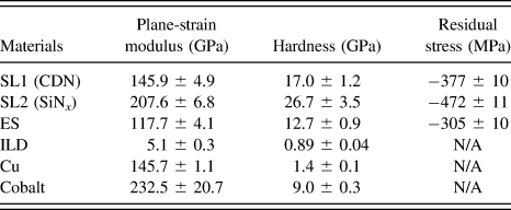
Figure 1 is a schematic illustration of the multilayer thin film stacks of the specimen for adhesion measurement at the metal/ES and ILD/ES interface; the latter can also be used for measuring the cohesive fracture energy of ILD material with the DCB technique. The multilayer stacks are fabricated on a 300 mm (100)-silicon wafer using industrial fab processes. A reference stack containing a thick ES layer (100 nm by default) is to be compared with a SL stack where the thickness of the ES layer is scaled down to 10 nm with single or dual SLs added. The default thickness of SL is 100 nm unless otherwise specified. Amorphous carbon-doped silicon nitride (CDN) and high density silicon nitride (SiNx) films are evaluated as candidate material for use as SL, which are deposited by plasma-enhanced chemical vapor deposition (PECVD) method. Electroplated Cu and chemical vapor deposited cobalt films are utilized as model metal materials; both layers were chemical–mechanical polished to the targeted thickness (220 nm for Cu, 120 nm for Cobalt) before the ES layer is deposited. The nanoporous ILD material is deposited by PECVD methods followed by UV curing, resulting in the final porosity of approximately 30% and thickness of 100 nm. Nanoindentation and wafer curvature techniques are used to characterize the plane-strain modulus and residual stress of the materials; results are summarized in Table I. In this work, all interfacial adhesion measurements are conducted with 4PB technique, and cohesive fracture energy of ILD is measured with DCB. 4PB and DCB specimens have been prepared with procedures described elsewhere.Reference Li, Tsui and Vlassak9,Reference Scherban, Xu, Merrill, Litteken and Sun26 Adhesion energy and cohesive fracture energy are calculated according to long established procedures,Reference Ma24,Reference Kanninen27 where the sandwiched multilayers are neglected in the calculation of steady-state energy release rate because they are orders of magnitude thinner than the silicon substrates. This simplification is validated by comparing the result with that calculated using a generalized formula where each individual layer is considered, which yields a relative difference less than 1% for stack of interest in this work.Reference Hsueh, Tuan and Wei28 Also note that epoxy bonding is used in this study instead of metallic diffusion bonding to form the sandwiched specimens shown in Fig. 1. The former has much reduced processing temperature (150 °C for 1.5 h) compared to the latter (usually 400 °C for 4 h or longerReference Ma24,Reference Dauskardt, Lane, Ma and Krishna29 ), and is expected to have lower impact, if at all, to the interface properties of interest. The resulting epoxy bond layer is approximately 1 μm thick. All samples are tested with a DTS delaminator (DTS, Menlo Park, CA) at 21 ± 1 °C. Relative humidity is controlled to be 40 ± 5% for 4PB test, and below 1% by nitrogen purging for DCB test. At least five samples are tested under each condition for statistics.
Summary of material properties.
III. RESULTS AND DISCUSSION
Figure 2 shows the representative load–displacement curves of 4PB test of the Cu/ES interface, with load value normalized by the sample width. Comparison is made between the reference stacks where ES thickness is varied from 10 to 200 nm and the SL stacks where ES thickness is fixed at 10 nm and SL thickness is varied from 100 to 500 nm. CDN is used as SL material in this case. Smooth load plateau, which signifies a steady-state delamination process, is obtained for the SL stacks, as well as for the reference stacks where the ES thickness is 100 nm or greater. The adhesion values extracted from the load plateau of the SL stacks agree well with each other and with those from the reference stack whose ES layer is 100 nm or greater, providing a consistent measurement of the Cu/ES adhesion while allowing the ES layer thickness to be scaled by 10 times. The fact that the 100 and 500 nm SL samples yield matched adhesion indicates that a 100 nm SL is thick enough to isolate the plasticity effects from the epoxy layer in this case. For tougher interfaces, however, a thicker SL may be needed. Another observation is that when the ES thickness in the reference stack is reduced below certain threshold value (between 100 and 30 nm), zigzag starts to appear in the otherwise load plateau regime with alternating linear increments and sudden drops, suggesting a stick-slip crack growth mechanism. The mean and fluctuation of the zigzag increases with thinner ES due to the reduced separation between the crack tip and the epoxy layer and a stronger dissipation effect induced by the relatively soft epoxy layer. This discrete crack propagation mode is well known for polymeric materials and interfaces and has been attributed to the dynamic interaction of the crack driving force and stress relaxation.Reference Kausch and Williams30 Postmortem optical fractography of the delaminated surface reveals extensive fragments as shown in the inset of Fig. 2, with periodic stripes corresponding to the transitions from “stick” to “slip” where crack velocity changes abruptly. The resulting crack path consists of interfacial delamination at the Cu/ES and ES/epoxy interface, mixed with cohesive fragmentation of the ES and epoxy layers. It is expected that more mechanical energy is dissipated in driving the crack to propagate in this mode than in the smooth steady-state mode observed in the SL stacks, for example, leading to an apparent increase of the interfacial adhesion. Understanding the delamination mechanism aside, such complicated mixture of several cracking modes is not very useful for measuring the intrinsic adhesion properties at Cu/ES interface.
4PB load–displacement curves of Cu/ES interface collected from the reference and the SL stacks. The curves from the SL stacks have been offset horizontally for clarity. The inset shows an optical microscopy image of the delaminated surface from the reference stack with a 10 nm ES (dummy side).
Cobalt is one of the candidate materials widely studied across the semiconductor industry for potential implementation as copper cap barrier or whole replacement of copper.Reference Hauschildt, Hintze, Gall, Koschinsky, Preusse, Bolom, Nopper, Beyer, Aubel and Talut31–Reference Yang, Baumann, Wang, Lee, Ma, AuBuchon and Edelstein33 Compared to copper, cobalt is mechanically stiffer and harder (see Table I), and can form a tougher interface with ES. Adhesion testing of the cobalt/ES interface has required further engineering of the SL stack due to the intrinsic properties of this interface and the pair of materials forming the interface. As shown in Fig. 3, the impinging precrack tends to penetrate through the ES layer than to propagate along the target interface if the reference stack or a CDN-SL stack is used. This tendency holds true regardless of the thickness of the CDN-SL and ES layer within the range studied but breaks down when CDN is replaced by SiNx as the SL. As summarized in Table I, SiNx has higher elastic modulus and more compressive residual stress than CDN film. With the SiNx-SL stack, steady-state interface debonding, manifested by the smooth load plateau, is obtained. The extracted adhesion values from the load plateau are consistent with each other independent of the SL thickness, indicating SL is sufficiently thick to block plastic dissipation of the epoxy layer. More importantly, the SL provides a knob to fine tune the tendency of interface delamination, by which one can design a stack to delaminate the cobalt/ES interface in a controlled fashion; without the SL, this interface cannot be delaminated even if thick ES is available.
4PB load–displacement curves of the Cobalt/ES interface collected from the reference and SL stacks with different SL materials and thicknesses. SL curves are offset for clarity.
Fundamentally, the path selection of the impinging crack at a bimaterial interface is governed by the competition of fracture driving forces and resistances to the penetrating or delamination crack. Penetration is favored over delamination if G d/G p < Γd/Γp, and vice versa.Reference He, Evans and Hutchinson34,Reference Ming-Yuan and Hutchinson35 Here, G d and G p are the energy release rate for driving delamination and penetration, respectively, and Γd and Γp denote the interfacial adhesion and fracture energy of the intact material (ES in this case). While Γd and Γp can be regarded as material constant for a given interface if their dependence on mode-mixity is neglected, G d and G p are complicated functions of the geometry (impinging angle, film thickness, defect sizes), material properties (elastic constants, residual stresses), and boundary conditions. Analytical solutions of G d/G p are available for asymptotic semi-infinite bilayer interfaces that account for the elastic mismatch,Reference Volinsky, Moody and Gerberich20 residual stresses,Reference Volinsky, Moody and Gerberich21 and split singularity.Reference Zhang and Suo36 However, Roham and Hight reported that the effect of finite film thickness, which is not captured by the asymptotic solutions, can be significant for multilayer 4PB specimen.Reference Roham and Hight37 For a stack similar to the reference stack in this study, their calculations show that G d/G p and thus the tendency for an impinging crack to induce delamination is enhanced by using a thicker and stiffer ES with higher compressive stress, which can be used to qualitatively understand the crack path selection behavior in Fig. 3. Suppose one can replace the ES/SL bilayer with a homogeneous layer whose effective properties are such that G d/G p remains the same as in the original bilayer structure. The thickness, residual stress, and elastic properties of the effective layer are determined by the ES and SL. Keeping ES fixed, one can modulate the effective thickness, elastic modulus, and residual stress of effective layer by changing that of the SL accordingly. Given that Γd and Γp are not affected by the SL, one would hence expect that delamination is promoted the most when using a SiNx SL, followed by the CDN SL, and is least favored when using the reference stack; this is consistent with our experimental observation.
We now proceed to demonstrate the usefulness of the SL stack for the low-k ILD/ES interface adhesion and ILD cohesive strength measurement. As the weakest material in the interconnect structure, ILD material and its interfaces are critical for the overall mechanical integrity of the interconnects. Due to the relatively weak adhesion at the ILD interface and high elastic mismatch with the ES, introducing an interfacial crack that propagates smoothly is usually not difficult. However, when the reference stack is used, the adhesion measurement starts to be increasingly affected by the bonding epoxy layer as the ES thickness reduces below about 100 nm, and manifests as an apparent increase of adhesion [see Fig. 4(a)] even if the interface chemistry and bonding are unchanged. With the introduction of SL between the ES and epoxy, adhesion results consistent with those from the thick-ES reference stack can be obtained. Plastic contribution to interface adhesion measurement arises from the yielding of the ductile layers especially the epoxy bonding layer adjacent to the high stress field of the propagating crack tip.Reference Dauskardt, Lane, Ma and Krishna29,Reference Hutchinson and Evans38,Reference Lane, Dauskardt, Vainchtein and Gao39 Delineation of the plastic contributions especially that from the bonding materials (epoxy or metallic bondingReference Dauskardt, Lane, Ma and Krishna29) is essential for establishing the relevance of the adhesion measurement for risk and failure analysis of actual interconnect structures. To this end, various micromechanics models based on cohesive zone simulations have been developed.Reference Dauskardt, Lane, Ma and Krishna29,Reference Hutchinson and Evans38,Reference Lane, Dauskardt, Vainchtein and Gao39 Nonetheless, detailed characterization of the elastic and plastic properties of the materials in the multilayer structure is needed to apply those models, which by itself is a challenge. The SL stack structure provides a pragmatic alternative approach to decouple plastic contribution for reliable adhesion measurement. Figure 4(b) shows the cohesive fracture energy of ILD measured using SL stacks compared to that from a reference stack. ES and SL thicknesses are denoted in the plot. It is clear that the SL stacks allow a 10x reduction of ES thickness yet provide consistent cohesive fracture energy measurement. In addition to the examples discussed in the study, we have recently reported that the SL structure can also be applied on single level dual damascene interconnect structures.Reference Li, Kobrinsky, Shariq, Richards, Liu and Kuhn25 Augmented with mode-mixity tuning using asymmetric DCB specimens, unprecedented level of fine control of the cracking behavior can be achieved, which provides the opportunity to test different materials and interfaces within integrated structures, including the metallization vias and low-k ILD.
(a) ILD/ES adhesion, and (b) ILD cohesive fracture energy characterized using reference and SL stacks. SL1 and SL2 refer to the lower and upper SL as shown in Fig. 1. (the lower-right stack). Adhesion and fracture energy are calculated with standard method as detailed in Ref. Reference Li, Tsui and Vlassak9.
IV. CONCLUDING REMARKS
In summary, we have demonstrated a novel strategy to control crack propagation in a multilayer stack by means of a SL stack structure. Dependence of fracture behavior on the thickness and material properties of the SL has been studied. By properly designing the SL, a number of challenges associated with fracture testing of ultrathin film stack and tough interface can be overcome. Reliably adhesion and cohesive fracture energy measurement are demonstrated for representative interconnect materials and interfaces. We anticipate that this work will have broad implications for the microelectronics industry to develop optimized processes and interfacial engineering strategies toward building more robust interconnects and integrated devices.
ACKNOWLEDGMENTS
H.L. acknowledges Portland Technology Development of Intel Corporation for supporting test wafers. Special thanks go to Jimmy Liu of Intel Corporation for 4PB and DCB testing.