Introduction
Transparent electrodes are ubiquitously used in optoelectronic devices where light must pass through a section, and current or voltage needs to be applied. These devices include thin-film solar cells (organic, inorganic, hybrid), displays (liquid-crystal display, plasma display, organic light-emitting diode [OLED]), touch screens (resistive, capacitive), electronic books, smart windows, flexible lighting, and passive devices (such as transparent heating, transparent speakers).Reference Hecht, Hu and Irvin1 The properties of transparent electrodes are extremely important for device performance, and the specifications vary based on types of devices. For example, while source roughness and work function are insignificant for resistive touch screens, they are crucial for OLEDs and organic solar cells.Reference Hecht, Hu and Irvin1 Moreover, the optical haze of particular transparent electrodes is beneficial for high-efficiency solar cells but problematic for certain types of displays. The mechanical properties of the electrode are crucial for flexible devices but not important for devices on rigid substrates. Across all devices, however, the optical transparency (T) and electrical sheet resistance (R s) are the two most important parameters. Unfortunately, these two parameters are in constant competition with one another. Since R s values are often reported at different transparencies, it is hard to compare two transparent electrodes directly, and hence a figure of merit (σdc/σop, where σdc is the dc conductivity, and σop is the optical conductivity) is widely used to evaluate the performance of transparent electrodes.Reference Hu, Hecht and Gruner2, Reference Rowell and McGehee3
Depending on the application, R s can range from 10 Ω/sq to 106 Ω/sq, but typically the transparency needs to be ≥90%. 106 Ω/sq is sufficient for antistatic applications, 400–1000 Ω/sq is sufficient for many touch screen applications, and ≤10 Ω/sq is needed for OLEDs and solar cells.Reference Hecht, Hu and Irvin1 Recently, Rowell and McGehee conducted a theoretical study on R s for thin-film solar cell modules. Their conclusion was that a competitive transparent electrode must have an optical transparency of at least 90% at an R s of less than 10 Ω/sq for monolithically integrated modules.Reference Rowell and McGehee3 Koishiyev and Sites conducted a similar study on the impact of R s in 2D modeling of thin-film solar cells.Reference Koishiyev and Sites4 Metal busbar fingers conduct current globally, and transparent electrodes conduct current locally. Assuming the current is distributed uniformly across the transparent electrode, the power loss associated with the sheet resistance of the transparent electrode is P = R sL 2J 2/3, where P is the power loss, J is the current density, and L is sub-cell length.Reference Koishiyev and Sites4 For high-efficiency solar cells, R s needs to be as low as possible to reduce power loss from transparent electrodes.
Over the past eight years, various types of transparent electrodes based on nanoscale materials have emerged. Percolative networks with randomly distributed carbon nanotubes (CNTs) have been extensively studied, and startups such as Unidym and Eikos have focused on commercializing the technology.Reference Hu, Hecht and Gruner2, Reference Wu, Chen, Du, Logan, Sippel, Nikolou, Kamaras, Reynolds, Tanner, Hebard and Rinzler5 However, due to the large tube-tube contact resistance, CNT-based transparent electrodes typically give the best performance of R s of 150 Ω/sq and optical transparency of 80%.Reference Hu, Hecht and Gruner6 In the past four years, graphene-based transparent electrodes have been investigated, and an excellent performance of 30 Ω/sq R s value and 90% optical transparency have been demonstrated for chemical vapor deposition-grown continuous graphene.Reference Bae, Kim, Lee, Xu, Park, Zheng, Balakrishnan, Lei, Kim, Song, Kim, Kim, Ozyilmaz, Ahn, Hong and Iijima7 For low-cost applications, solution-processed films with graphene flakes are more attractive, and the best performance until now is in the range of 200–300 Ω/sq and 80%.Reference Wassei and Kaner8 These carbon nanostructure–based transparent electrodes show excellent mechanical flexibility and are promising for touch screens and flexible devices. Unfortunately, their T/R s performance does not meet the requirements for many other applications, such as solar cells. To achieve the highest performance in optical transparency and sheet resistance, metal-based nanostructures need to be used to their highest electrical conductivity at room temperature. In this review, we summarize recent research on nanostructured metallic transparent conductors, which includes structure design, fabrication, properties, device integration, future challenges, and the potential for flexible electronics and next-generation solar cells.
Metal thin films
Due to their high free-electron density, metals have the highest conductivity among materials at room temperature. As another consequence, bulk metals are highly reflective in the visible range and cannot function as a transparent electrode. Like many other materials, metals become more transparent as the thickness decreases down to the tens of nanometers range. Such ultrathin metals have been explored as transparent electrodes and can in fact be purchased. Pipe and ShteinReference O’Connor, Haughn, An, Pipe and Shtein9 reported a summary of transparent electrodes based on nonpatterned metal films, where the R s value is approximately 10 Ω/sq for a nonpatterned metal film with a thickness of around 10 nm. However, as film thickness decreased from approximately 20 nm, R s sharply increased due to electron scattering from the surface because of substrate and grain boundaries. This mechanism has been previously investigated and is explained by the Fuchs-Sondheimer and Mayadas-Shatzkes models.Reference O’Connor, Haughn, An, Pipe and Shtein9 As the thickness of the metal becomes less than 10 nm, the metal thin film becomes more transparent; however, the sheet resistance increases dramatically with decreasing thickness. This thickness-dependent transport makes thin metal films less attractive for transparent electrode applications.
In a separate study, Pruneri et al. also investigated the potential of ultrathin metal films for transparent electrodesReference Ghosh, Martinez, Giurgola, Vergani and Pruneri10 and found that a sputtered metal thin film with a thickness of less than 10 nm formed a uniform and continuous film over a 10 cm substrate. In addition, they found Ni films with a thickness of 2–10 nm have an average visible transmittance between 40–80% and sheet resistance between 30–1200 Ω/sq. These metal thin films are highly transparent in the UV and IR wavelength range and hence are attractive for many applications such as IR detectors and IR solar cells. Transparent window films based on metals are commercially available, and both silver and gold films on plastic poly(ethylene terephthalate) substrates are also available. Compared with Ni film, these silver and gold films have a much better performance in terms of T/R s due to their high electrical conductivity. Typical R s and T values for transparent electrodes based on silver or gold is 4.5–9 Ω/sq and 75%, respectively.Reference Hecht, Hu and Irvin1
Metal nanogrids
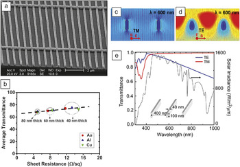
In an effort to achieve the best metal-based transparent electrode, nanostructures can be employed. One model structure is a metal nanogrid with periodic metal lines. Such nanostructures provide opportunities to manipulate photons and electrons to achieve unique properties that are not possible for a flat indium tin oxide (ITO) electrode. Because the thickness of the metal lines is much larger than that of metal films, electron scattering due to the substrate roughness and the strain boundaries decreases, and therefore the conductivity is close to that of the bulk counterpart. Light scattering and coupling in such nanogrids also provides additional benefits for device applications, particularly for solar cells where light scattering enhances the absorption of the active layer. As noted by Guo et al., two design considerations must be made for nanogrid-based transparent electrodes: (1) the line width of the metal mesh is subwavelength to provide sufficient transparency; (2) the period of the mesh is submicrometer to ensure the uniformity of the current across the active layer.Reference Kang, Park, Ahn, Xu and Guo11 Excellent performance has been achieved based on such metal nanogrids (Figure 1a and 1b).
(a) Scanning electron microscopy image of an as-fabricated metal electrode. (b) Average transmittance versus sheet resistance of metal grids with a line width of 120 nm.Reference Kang and Guo17 Absolute value of the modeled optical electric field and power flow for light (600 nm wavelength) incident on a freestanding Ag grating (400 nm period, 40 nm line width, 100 nm high) for both (c) transverse magnetic (TM) and (d) transverse electric (TE) polarization. (e) Simulated transmittance versus wavelength for two modes. The AM1.5 solar irradiance data (black line) are plotted for comparison.

Catrysse and Fan performed a calculation with a finite-difference frequency-domain method for nanopatterned metallic films as a transparent conductor in optoelectronic devices and found an R s value of 0.8 Ω/sq and a T value of 90% to be achievable for nanopatterned silver films.Reference Catrysse and Fan12 Moreover, Cui and Peumans calculated the optical electrical field and power flow for silver nanogrids (Figure 1a and 1b).Reference Lee, Connor, Cui and Peumans13 Finite-element modeling was used to calculate the transmittance of metal nanogrids as a function of the geometric parameters. In Figure 1c and 1d, the line width is 40 nm, the period is 400 nm and the height is 100 nm, and the theoretical R s is 1.6 Ω/sq. Figure 1e shows the transmittance for transverse electric (TE) and transverse magnetic (TM) modes from the modeling.
Various methods for fabricating such metal nanogrids have been reported.Reference Kang, Park, Ahn, Xu and Guo11, Reference Park, Kim, Constant and Ho14, Reference Ahn and Guo15 Guo et al. pioneered nanoimprint lithography, and using this method, they demonstrated excellent results on various metals and substrates and also showed applications in solar cells and LEDs. Recently, they have developed large-area continuous imprinting of nanogrids using their apparatus that is capable of roll-to-roll printing on flexible web and roll-to-plate printing on rigid substrates.Reference Ahn and Guo16 In addition, they developed a different nanopatterning method, localized dynamics wrinkling, which creates continuous metal nanogratings by simply sliding a flat edge of a hard material on a thin metal coated polymer layer.Reference Ahn and Guo15
Toward low cost: Solution-processed silver nanowire network
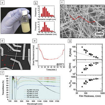
While metal nanogrid-based transparent electrodes demonstrate excellent performance and are ideal for fundamental simulations, the fabrication process is often costly, and vacuum deposition is needed, making them unrealistic for practical applications. For low-cost applications, solution-based high-speed roll-to-roll processing is preferred. Recently, networks of randomly distributed metal nanowires, especially silver nanowires (Ag NWs), have been explored as an emerging candidate since these networks maintain the advantages of patterned nanogrids such as high transparency, low sheet resistance, and mechanical flexibility.Reference Lee, Connor, Cui and Peumans13 The keys to this technology include the growth of Ag NWs with small diameters in solution, stable nanoink formulation, scalable coating, decrease of junction resistance, and patterning. Ag NWs were synthesized by the reduction of silver nitrate in the presence of poly(vinyl pyrrolidone) (PVP) in ethylene glycol.Reference Lee, Connor, Cui and Peumans13 Figure 2a shows an Ag NW ink in methanol with a concentration of 2.7 mg/mL. The distributions of nanowire length and diameter are shown in Figure 2b. The percolation theory for one-dimensional sticks predicts that the percolation threshold, Nc, dramatically decreases as the length of the sticks increases.

(a) Ag nanowire (NW) ink in ethanol solvent with a concentration of 2.7 mg/mL. (b) The Ag NW length and diameter histogram. (c) Scanning electron microscopy images of an Ag NW mesh on a plastic substrate. The red dashed line indicates the electron transport path. (d) Electrical measurement of individual Ag NWs and a junction. (e) Sheet resistance versus annealing time for an Ag NW mesh annealed at 200°C. (f) Optical transmittance of transparent Ag NW electrodes measured with a UV-vis spectrometer, without including the substrates. Indium tin oxide on poly(ethylene terephthalate) is obtained from CPFilms. (g) Sheet resistance R s, σdc, and σdc/σop, where σdc is the dc conductivity and σop is the optical conductivity, for different film thickness.

From this theory, longer and thinner Ag NWs with smooth surfaces are preferred. Various deposition methods have been explored for fabricating Ag NW electrodes from solution such as Mayer rod coating, filtration, and drop coating. Figure 2c shows an Ag NW network. Charge transport happens along the Ag NWs. Due to the PVP coating on the surface, the junction resistance is typically high, ∼1 GΩ, and limits the overall conductance of the network. Various methods to decrease the junction resistance have been developed, such as electrochemical annealing, heat treatment, and rapid thermal annealing.Reference Hu, Kim, Lee, Peumans and Cui18 Resistance of a single junction between two nanowires can be monitored in a device with metal contacts fabricated by e-beam lithography (Figure 2d). For example, R s decreases dramatically (from >1000 Ω/sq to 100 Ω/dq) upon heating at 200ºC for 20 minutes, due to the fusion of the Ag-Ag junction through the insulating PVP layer. Further heating leads to increases in the resistance, which is due to the coalescence of the Ag NWs. Cui et al. performed a comprehensive study on scalable coatings and the properties of Ag NWs, including the flexibility of different bending radius, adhesion, and stability toward various chemicals/temperature.Reference Hu, Kim, Lee, Peumans and Cui18
Solution-processed Ag NW electrodes show excellent performance in terms of transparency and sheet resistance. Coleman et al. prepared films with an R s value of 85% and a T of 13 Ω/sq and showed the films to be electromechanically robust (no change in resistance after being bent more than 1000 cycles).Reference De, Higgins, Lyons, Doherty, Nirmalraj, Blau, Boland and Coleman19 Figure 2e shows the specular transmittance of Ag NWs with different R s. The sheet resistance and transparency in the visible range of the Ag NW electrode are comparable to those of the ITO electrode. Also the transmittance curve of the Ag NW electrode is flat in the near infrared regions, while the transmittance for the ITO electrode decreases for wavelengths >1100 nm (Figure 2g). One figure of merit for comparing different transparent electrodes is σdc/σop, which was first used by Gruner et al.Reference Hu, Hecht and Gruner2 Here, σdc and R s are highly thickness-dependent. Coleman studied the thickness dependence of R s, σdc, and σdc/σop and found that a high figure of merit, 500, was achieved for thick Ag NW films.Reference De, Higgins, Lyons, Doherty, Nirmalraj, Blau, Boland and Coleman19 This is much higher than other transparent electrodes (nanotube ∼25 and graphene ∼0.5).
Toward low cost: From silver to copper
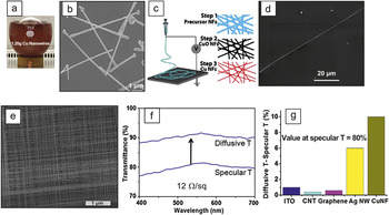
Solution-processed silver nanowire thin films exhibit electrical and optical properties comparable with ITO. However, silver is also similar to ITO in price ($500/kg) and scarcity. Copper possesses a comparable conductivity with silver, is 1000 times more abundant than indium or silver, and is 100 times less expensive. Therefore, copper-based nanomaterials hold great promise as cheap and scalable transparent electrodes. As a result, research has been focused toward designing and constructing copper-based one-dimensional nanostructures. Zeng et al. demonstrated that copper nanowires (Cu NWs) can be synthesized by a simple room-temperature solution process.Reference Chang, Lye and Zeng20 The synthesized Cu NWs have a single crystalline structure with diameters of 90 ± 10 nm and a length ∼10 um. However, in Zeng’s work, only a limited amount of Cu NWs (<10 mg) was synthesized. Recently, Wiley et al. scaled this reaction by 200 times and therefore made Cu NWs possible for transparent electrode applications (Figure 3a and 3b).Reference Rathmell, Bergin, Hua, Li and Wiley21 In their work, >1 g of Cu NWs was synthesized by solution processing. The copper NWs were then printed on glass substrates to form a transparent conducting layer. The Cu NW film transparent electrodes have a sheet resistance of ∼20 Ω/sq at 60% transmittance. The low transmittance of Cu NWs can be attributed to their low aspect ratio. Generally, a Cu NW has a diameter of ∼100 nm and a length <20 um.
(a) Picture of the reaction flask after growth of Cu nanowires (NWs) at 80°C for one hour. (b) Scanning electron microscopy (SEM) image of short Cu NWs. (c) Schematic of materials preparation method. Left side: Schematic of an electrospinning setup, shown without a syringe pump; right side: the fabrication process of Cu nanofibers (NFs). (d) SEM image showing the continuous structure of a Cu NF, indicating a length that easily exceeds 100 μm. (e) SEM image of a Cu NF grid. (f) Diffusive transmittance is higher than specular transmittance in Cu NF electrodes. (g) The difference between diffusive transmittance and specular transmittance for different transparent electrodes.

From percolation theory, a larger aspect ratio (lower diameter or larger length) of Cu NWs leads to transparent electrodes with better performance. However, the length of solution-processed Cu NWs is limited by the synthesis method. Recently, Cui et al. employed an electrospinning method to achieve continuous Cu nanofibers (NFs).Reference Wu, Hu, Rowell, Kong, Cha, McDonough, Zhu, Yang, McGehee and Cui22 Electrospinning is currently the most powerful technique that allows fabrication of nanoscale, continuous, ultralong fibers. It employs a strong electrical field to draw fine fibers from a liquid source (Figure 3c). Electrospinning has been explored as a fast and efficient process to fabricate continuous 1D nanomaterials.Reference Li and Xia23 The fabrication process for electrospinning Cu nanofiber transparent electrode is described on the right side of Figure 3c. In step 1, precursor nanofibers with copper acetate dissolved in poly(vinyl acetate) (PVA) are electrospun onto a glass substrate, the fibers have diameters of around 200 nm. In step 2, polymer nanofibers with copper precursors are heated at 500°C in air for 2 h to remove all the polymer components, and the nanofibers are transformed to dark brown CuO nanofibers. In step 3, CuO nanofibers are reduced into red Cu nanofibers after annealing in an H2 atmosphere at 300°C for 1 h. The length of electrospun Cu NFs can be much larger than solution-processed Cu NWs. Figure 3d shows a single electrospun copper NF, with a diameter of 80 nm and a length >100 um. Typically, values for R s and T are 200 Ω/sq at ∼96%, 50 Ω/sq at ∼90%, and 12 Ω/sq at ∼80% for Cu NF transparent electrodes at room temperature. Electrospinning can also provide a facile process to align NFs to form regular arrays (Figure 3e). In such directional NF systems, the charge carriers are transported primarily along the fibers with little junction scattering. The nearly junction resistance-free network with oriented NFs can greatly enhance the surface conductance in the orientation direction with a shorter conduction path compared with a random network. Due to the metallic nature of these films, light scattering is significant. There are two types of transmittance: specular transmittance (the normal and forward direction) and diffusive transmittance (all in the forward direction). The difference between the two types of transmittance is the portion of scattered light in the forward direction. The transparent Cu NF electrodes show higher diffusive transmittances than specular transmittances. The difference is 10% at ∼80% specular transmittance and 4% at ∼90% specular transmittance (Figure 3f). Such transparent electrodes with large light scattering (Figure 3g) can help light absorption in the active layer, and therefore make Cu NF transparent electrodes suitable for solar cell systems.
Device integration
Metal nanostructure-based transparent electrodes exhibit excellent performance in terms of optical transparency, electrical conductance, and mechanical flexibility. They will find applications in many optoelectronic devices such as displays, touch screens, and solar cells.Reference Hecht, Hu and Irvin1 Many proof-of-concept devices such as solar cells and light-emitting diodes (LEDs) with incorporated transparent metal electrodes have been demonstrated. The following must be considered when these metal nanostructures are incorporated into devices: (1) surface roughness; (2) step coverage; (3) contact resistance; (4) interface, including conformal coating and charge transfer; (5) work function; and (6) process compatibility. Among all the emerging transparent electrodes, metal nanostructures have the lowest R s, which is particularly attractive for solar cell applications. When diffusive transmittance is used, an R s value of 10 Ω/sq and a T of 90% is readily achieved for Cu NF electrodes that meet the requirements for solar cells.
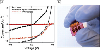
Peumans and Cui have demonstrated high-performance organic solar cells with an Ag NW mesh.Reference Lee, Connor, Cui and Peumans13 Figure 4 shows the device characteristics (a) and a photo of a flexible solar cell (b). Compared with an ITO-based device, the Ag NW-based solar cell has a higher short circuit current, which is attributed to the high optical transmittance, improved absorption of the active layer due to light scattering, increased surface roughness, and a local enhancement of optical intensity near Ag NWs. Separately, Guo et al. conducted a comprehensive study utilizing metal nanogrids for solar cells and performed detailed simulations based on rigorous coupled wave analysis to examine the optical absorption enhancement in their periodic Ag NW array-based organic solar cells.Reference Kang, Park, Ahn, Xu and Guo11, Reference Kang, Xu, Park, Luo and Guo24 They found that the peak enhancement integrating TM and TE modes reached 250% around the wavelength of 530 nm, which was due to plasmonic effect, as compared with ITO-based devices. They also found that the maximum fields concentrated near the edges of the bottom and top of Ag NWs for TM mode and is between the cathode and NWs for TE mode. The increase of short circuit current density for devices with metal nanostructures as transparent electrodes is important for achieving high-efficiency solar cells. However, solar cells with metal nanostructures show high dark current and lower open circuit voltage that is likely due to the current shunt paths as a result of the surface roughness. Methods to reduce the surface roughness are needed.
(a) Current density versus voltage for organic photovoltaic cells with a device structure of 45 nm CuPc/45 nm PTCB/10 nm BCP/100 nm Ag on an Ag nanowire (NW) mesh and indium tin oxide (ITO) in the dark and under 65 mW/cm2 illumination. (b) Photograph of a flexible solar cell based on a transparent Ag NW electrode.

Summary and perspective
Metal nanostructures such as nanogrids, nanowires, and nanofibers are promising candidates for next-generation transparent electrodes. Compared with other transparent electrodes, these metal-based transparent electrodes have the best performance in terms of optical transparency and sheet resistance. Due to the large scattering effect, these transparent electrodes are particularly useful for solar cell applications. Challenges such as long-term environmental stability, contact resistance between electrode and active materials, electrical shorting problems due to their large aspect ratio, uniformity, defects, and scalable fabrication must be overcome to fully integrate these new electrodes into commercial devices. Due to their low cost and the existing roll-to-roll fabrication capability in industry, transparent electrodes based on metal nanostructures will have future applications.
Acknowledgment
We acknowledge support from the King Abdullah University of Science and Technology (KAUST) Investigator Award (No. KUS-11–001–12) and U.S. Department of Energy.