I. INTRODUCTION
Many rare-earth (RE) metal silicides form self-assembled nanowires (NWs) on the Si(001) surface.Reference Preinesberger, Vandré, Kalka and Dähne-Prietch1–Reference Nogami, Liu, Katkov, Ohbuchi and Birge3 NW formation is due to an anisotropy in the lattice mismatch between the silicides and the silicon substrate. Nanosized compact silicide islands with much smaller aspect ratios are also observed under some growth conditions.Reference Eames, Reakes, Tear, Noakes and Bailey4 In many of these RE silicide systems, there are several different polymorphs that exist very close to the composition RESi2. These phases have different lattice constants and, thus, have different lattice mismatches with the substrate.Reference Houssay, Rouault, Thomas, Madar and Senateur5 For NW-forming RE silicides, it is generally the hexagonal phase that has one lattice constant very closely matched with the substrate. NW growth occurs along the direction of small lattice mismatch, whereas lateral growth is constrained by a strong lattice mismatch in the perpendicular direction.
Annealing NWs can lead to the transformation of the NWs into rectangular islands.Reference Liu and Nogami6 Previous cross-sectional transmission electron microscopy (TEM) studies on such samples show the existence of both hexagonal and nonhexagonal silicide phases.Reference Ye, Nogami and Crimp7–Reference Zhang, Crimp, Cui and Nogami9 From scanning tunneling microscopy (STM) and TEM measurements on the same sample, it can be inferred that the nanostructure morphology is correlated with the underlying silicide crystal structure.Reference Ye, Crimp and Nogami8
In this study, nanobeam electron diffraction (NBD) is used in plan-view TEM to study the epitaxy of GdSi2 nanostructures grown on Si(001). In NBD, information can be collected from single selected nanostructures, allowing direct correlation between the morphology of the nanostructures and the crystal structures. Consistent with prior work in other RE silicide systems, the NBD data presented show that the Gd silicide NWs have the hexagonal crystal structure, whereas the islands have the orthorhomic/tetragonal structure (these two phases have very similar lattice parameters, making them difficult to distinguish, and will be referred to as orth/tet hereafter). This analysis also confirms the relationship between silicide morphology and lattice mismatch, showing that the nanostructure morphology is controlled by the magnitude and direction of the lattice mismatch with respect to the silicon. STM data show that phase transformation from the hexagonal to the orth/tet phases can occur at the intersections of two NWs from neighboring Si(001) terraces.
II. EXPERIMENTAL DETAILS
The GdSi2 nanostructures were grown by metal deposition onto the Si(001) surface at 650 °C in ultrahigh vacuum (UHV). Some samples were annealed in-situ after deposition. The base pressure of the vacuum system was 2.0 × 10⁻¹⁰ Torr. The silicon substrates were precleaned by flashing up to 1175 °C in UHV. The typical Gd coverage was 1.5 monolayer (ML) [1 ML = 6.78 × 10¹⁴ atoms/cm2 surface atomic density on Si(001)], calibrated by a quartz crystal thickness monitor. STM was carried out at room temperature in the UHV chamber. Tunneling voltages were typically in the range |Vsample| ≤ 2.5V, with the tip at ground meaning that negative (positive) bias corresponds to empty (filled) states imaging, and tunneling currents were in the range 0.1 ≤ I ≤ 1.5 nA. None of the measurements reported here were particular sensitive to bias.
After STM imaging, samples were then removed from UHV for TEM sample preparation and characterization. Plan view samples were thinned by dimpling and ion milling from the back side of the substrate using a Gatan PIPS (Gatan, Pleasanton, CA). TEM images were collected using a JEOL 2200FS working at 200KV (JEOL Ltd., Tokyo, Japan).
III. RESULTS
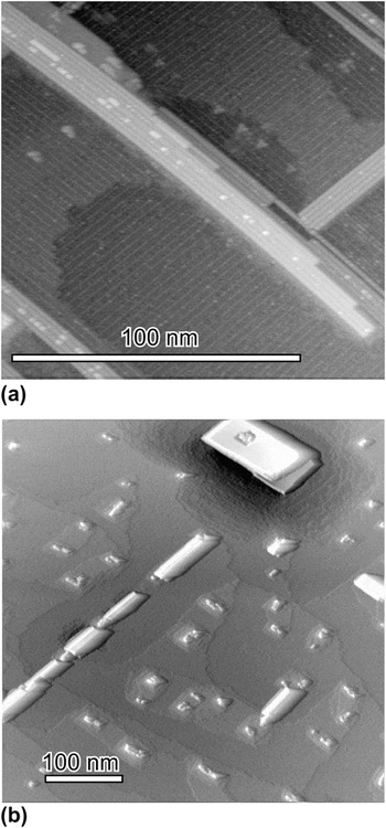
Figure 1 shows two typical STM images of GdSi2 nanostructures grown on Si(001). The general morphology of the surface is consistent with what has been reported in prior STM studies.Reference Lee and Kim10–Reference Ye, Crimp, Nogami, Ozkan, Rosei, Lopinski and Wang12 Figure 1(a) shows an image of a sample with ∼0.5 ML of Gd deposited at 600 °C, and Fig. 1(b) shows an image of the same sample after annealing at 650 °C for 1 h. In Fig. 1(a), only NWs are present. In general, the width of a single GdSi2 NW ranges from 1 to 3 nm, with lengths reaching one micron. However, NWs tend to grow together and form NW bundles. The NW bundles are typically one or two atomic layers high (one layer = 0.3 nm). Figure 1(b) shows that islands develop after annealing, whereas NWs disappear. The silicide islands are wider (>10 nm) and higher (>5nm) than the NWs and have smaller aspect ratios (<1:10). The maximum dimensions of the islands are usually less than 100 nm. Similar behavior as a result of annealing has been seen in other RE silicide systems.Reference Liu and Nogami6
Scanning tunneling microscopy (STM) images of Gd silicide nanostructures grown on Si(001). (a) (150 × 150 nm) as-deposited at 600 °C (V = −1.9 V; I = 0.11 nA), and (b) (500 × 500 nm) after annealing at 650 °C for 1 h (V = −1.6 V, I = 0.09 nA). The latter image has been rendered with simulated lighting to clarify the shape of the large three-dimensional island.

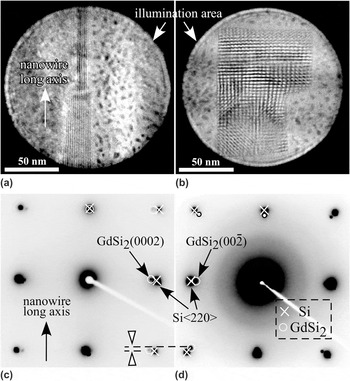
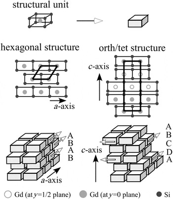
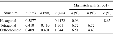
Figure 2 shows a NW (a) and an island (b) and their respective NBD patterns in (c) and (d). The upper panels [(a) and (b)] show the areas illuminated on the silicides and also reveal Moiré patterns resulting from the mismatch between silicide and substrate. The NBD patterns in the lower panels [(c) and (d)] show differences in the locations of the diffraction spots. For the NW, the GdSi2 diffraction spots associated with diffracting vectors g perpendicular to the long axis sit inside of the silicon spots, (measured as a large lattice mismatch of 9.3% with respect to the silicon), while no visible mismatch is seen along the long axis. The diffraction spot locations and corresponding mismatches are consistent with those expected from the bulk lattice constants of Si and the hexagonal silicide (Table I). Hence, the NWs are identified as the hexagonal phase. The combination of the images and NBD patterns also show explicitly that the long NW dimension corresponds to the small mismatch direction, whereas the short dimension forms along the large mismatch direction. This is also consistent with the appearance and spacing of the Moiré fringes seen in the nanostructure images. By contrast, an apparent mismatch exists in both Si<110> directions for the island, measured as 6.9% and 5.6%. This is consistent with the islands being the orth/tet phases. This relationship between the nanostructure morphology and the crystal structure, combined with the observation that islands are formed at the expense of NWs during annealing, suggests that the hexagonal phase can transform into the orth/tet phases. In fact, as pointed out by Harrison and Boland,Reference Harrison and Boland11 the conversion to orth/tet with annealing implies that the orth/tet phase is in fact thermodynamically favorable, consistent with thin film reaction studies.Reference Molnar, Gerocs, Peto, Zsoldos, Jaroli and Gyulai13 To illustrate the phase transformation, the hexagonal and orth/tet crystal structures are redrawn in Fig. 3 in terms of stacking arrangements of the same structural unit, a parallelepiped with silicon atoms at the apexes, and a rare-earth atom at the center.Reference Houssay, Rouault, Thomas, Madar and Senateur5 The hexagonal and orth/tet structures have only slightly different dimensions of these structural units. It is clear that the hexagonal structure is stacked with structural units with a consistent shifting perpendicular to the c axis (ABAB…—stacking order), whereas the orth/tet structure has an alternative stacking along the a and b axes (ABCDABCD…—stacking order). Hence, the phase transformation can be expressed in terms of a change in the structural unit stacking order.
Comparison of nanobeam diffraction (NBD) patterns from a nanowire (NW) and an island. (a) and (b) show the NW and island studied, with Moiré fringes evident, and (c) and (d) show the corresponding NBD patterns. Silicide and substrate diffraction dots are marked by small circles and crosses, respectively, in part of both patterns.

The crystal structures of hexagonal and orth/tet GdSi2, expressed in terms of stacked rectangular prism subunits, each with a Gd atom in the center and Si at the corners (after Ref. Reference Eames, Reakes, Tear, Noakes and Bailey4). The hexagonal structure is composed of subunits consistently shifted along the a axis (ABAB…); the orth/tet structure is composed of subunits with alternate shifting along the a and b axes (ABCDABCD…). The shaded center atoms indicate a shift perpendicular to the plane of the page.

Lattice parameters for bulk GdSi2 and lattice mismatches with respect to Si(001).

The Si(001) surface is terminated in rows of Si dimers that rotate 90° at a single height atomic step; this is a reflection of the diamond structure of bulk Si. Therefore, GdSi2 NWs nucleated on neighboring terraces grow in perpendicular directions. Hence, it is possible for NWs from neighboring terraces to intersect at the terrace edge.
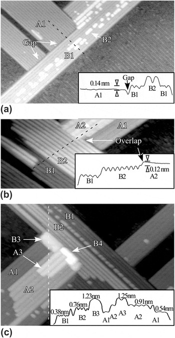
Figure 4 presents typical examples of NW intersections. When two single-layer NWs (labeled as nanowire A and nanowire B) come together at a single height step [Fig. 4(a)], there is often a gap between the NWs, resulting from the difference in registry of the atoms on different terraces. However, when second layer NW growth is present, as shown in Fig. 4(b), this gap disappears. In this example, the second layer of nanowire A (labeled A2) overgrows a portion of nanowire B (B2). When additional layers are added, the overgrowth of one NW on the other continues as seen for the third and fourth NW layers in Fig. 4(c). Here, the third layer of nanowire A (A3) protrudes into nanowire B. However, the fourth layer of nanowire B (B4) in turn grows on top of, but perpendicular to, A3.
STM images of NW junctions, with height profiles shown as insets. (a) Two single-layer-thick NW bundles on adjacent terraces (V = +0.42 V; I = 1.89 nA). (b) Two groups of NWs that are two-layer high at the intersection (V = −1.43 V; I = 1.1 nA); in this case, there is no gap, and the A2 layer grows over a part of B2. (c) Multiple-layer high NWs, with small rectangular islands visible at the intersection (V = −1.43 V; I = 1.1 nA).

Close examination of the step height in these images provides additional information. First, the height difference between equivalent structures across a single height substrate step agrees with the Si single step height (0.136 nm) to within measurement error of ±0.02 nm, as shown in the inset STM profiles in Figs. 4(a) and 4(b). Second, the step height difference between different layers of NW growth (e.g., between A1 and A2, or B1 and B2) is 0.37 ± 0.02 nm, which is in rough agreement with the height of a single unit cell of hexagonal silicide (0.3325 nm). However, this behavior changes at the third layer of silicide growth. For example, the inset in Fig. 4(c) shows that B3 is 0.47 nm above B2. At the same time, there is a morphological change; NW-like overgrowth is characterized by individual NWs separated by trenches, as seen in A1, A2, A3, B1, and B2. However, areas B3 and B4 do not have trenches, and they are compact rectangles; both of these characteristics suggest a transition to the orth/tet structure.
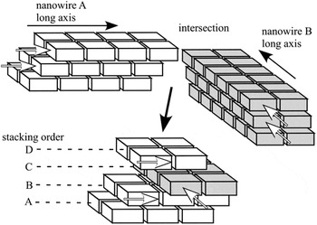
The alternating overgrowth of layers from two intersecting NWs may result in the NW structural units around the NW junctions being stacked similarly with those of the orth/tet phases (Fig. 3), as shown schematically in Fig. 5. Hence, the phase transformation from the hexagonal to the orth/tet phases is possible at the NW intersections and may originate from a stacking change in the silicide structural units. It should also be noted that the structural change only occurs at a minimum of three layers of silicide. It is clear from the crystal structure diagrams shown in Fig. 3 that the distinction between the hexagonal and the orth/tet phases only arises after stacking three layers of structural subunits.
A schematic of the intersection of two NWs. The structural units of each of the two individual NWs (A and B) are always shifted consistently along the NW long axis (or the a axis). Hence, at the intersection of two NWs, the structural units can shift in directions both a parallel and a perpendicular to the original direction of a NW, resulting in a local stacking arrangement consistent with that of the orth/tet bulk silicide structure.

This phase transformation mechanism reveals how single height atomic steps on Si(001) can nucleate growth of islands (orth/tet phase) on NWs (hexagonal phase). However, it is not possible to draw a simple correspondence between the density of NW intersections on a sample, and the resulting density of islands after annealing. First, there is a diversity of types of NW intersections, as shown in Fig. 4, and the degree to which islands nucleate at a given intersection is sensitive to the metal coverage. Second, depending on annealing duration and temperature, Ostwald ripening decreases the density of islands, as can be seen in Fig. 1.
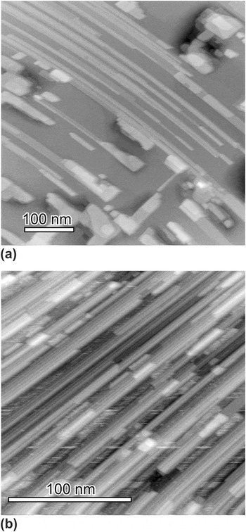
Nevertheless, these results do suggest a way to conduct selective growth of silicide nanostructures. It is well known that on vicinal Si(001), where the surface normal is tilted at least 4° from [001] along a <1–10> azimuth, the atomic steps on the surface pair up, resulting in a single domain, twofold symmetry surface.Reference Wierenga, Kubby and Griffith14 On such a surface, growth of Dy or Gd silicide results in a parallel array of NWs.Reference Liu and Nogami15–Reference Lee, Kim, Bae, Kim, Ragan, Ohlberg, Chen and Williams17 By choosing vicinal Si(001) as a substrate, the phase transformation from NWs to islands should be reduced because of the much lower density of single height atomic steps that would generate NW intersections. Figure 6 shows STM images of GdSi2 grown on Si(001) and vicinal Si(001) under similar conditions. Usually, postgrowth annealing between 600 and 650 °C substrate temperature converts a significant fraction of grown NWs to islands on a nonvicinal Si(001) surface, as seen in both Figs. 1 and 6(a). However, it is evident that there are no islands on the vicinal Si(001) sample following similar annealing conditions.
Comparison of Gd silicide nanostructures grown on Si(001) and vicinal Si(001) substrates. (a) (500 × 500 nm) ∼1.5 ML Gd deposited on Si(001) at a growth temperature of 650 °C (V = −2.5 V; I = 0.09 nA); (b) (150 × 150 nm) ∼1.0 ML Gd deposited on vicinal Si(001) at 650 °C (V = −2.1 V; I = 0.09 nA). Both of these samples were annealed for 20 min after growth.

IV. CONCLUSIONS
Explicit crystallographic information of GdSi2 nanostructures grown on Si(001) is presented in this article. Nanobeam diffraction analysis reveals that islands correspond to the orthorhombic or tetragonal phases of the silicide, whereas NWs have the hexagonal crystal structure. Phase transformation from the hexagonal to the orth/tet phase is observed at perpendicular intersections of silicide NWs. This transformation originates from the overgrowth of intersecting silicide layers at the NW junction. This mechanism explains why NW growth is facilitated by growth on vicinal Si(001) substrates.
ACKNOWLEDGMENTS
This work was supported by the NSF through Grant No. DMR-0305472. The JEOL 2200FS TEM was acquired in part by funds from NSF Grant No. DMR-0079578. Jun Nogami acknowledges support from the National Sciences and Engineering Research Council (NSERC) Canada.