I. INTRODUCTION
The large tunability of permittivity and the relatively low dielectric loss at microwave frequency of SrTiO3 (STO) and (Ba, Sr)TiO3 thin films have fostered great interest in their applications in microwave-tunable devices.Reference Vendik, Hollman, Kozyrev and Prudan1–Reference Pertsev, Tagantsev and Setter3 However, experimental and theoretical studies demonstrated that strains, induced by lattice mismatch between these ferroelectric films and their substrates, strongly affect their dielectric properties. To resolve this, different relaxation techniques were assessed, such as using different substrates, post-annealing, adding interface layers, applying oxygen partial pressure, and changing film thickness.Reference Canedy, Li, Alpay, Salamanca-Rica, Roytburd and Ramesh4–Reference Park, Peterson, Jia, Lee, Zeng, Si and Xi7
Earlier, we proposed a two-step growth method to mitigate strains in STO thin film, starting growth in the first step at a lower temperature to obtain a high nucleation density, followed by second-step growth at high temperature. We demonstrated an effective reduction in strain in epitaxial STO thin films on a LaAlO3 (LAO) substrate using pulsed laser deposition (PLD).Reference Yamada, Astafiev, Sherman, Tagantsev, Muralt and Setter8, Reference Yamada, Astafiev, Sherman, Tagantsev, Su, Muralt and Setter9 We found that a 10-nm first layer (FL) can almost completely relax the strain induced by lattice mismatch between the film and its substrate. The two-step-grown STO film exhibited substantially higher permittivity and tunability than the conventional films grown by a single-step process, which were under compressive strain. We interpreted these dielectric responses of both types of film by Landau’s theory, taking account of the difference in the residual strain in them.Reference Yamada, Sherman, Su, Tagantsev, Muralt and Setter10 To further understand the mechanism whereby the two-step growth process induces substantial strain relaxation, we undertook a comprehensive study on the microstructure of the STO film, as reported herein.
Generally, there are three typical modes of growthReference Freund and Suresh11: (i) two-dimensional (2D) layer-by-layer growth (the Frank der Merwe mode.); (ii) three-dimensional (3D) island growth (the Volmer–Weber mode); and (iii) the 2D–3D island-on-layer growth [the Stranski–Krastanov (SK) mode]. For single-step STO thin films grown by PLD under our experimental conditions, seemingly growth follows the SK mode, as indicated by the existence of dislocations and the enhanced surface roughness. In contrast, for films generated via two-step growth, the amorphous-FL is being crystallized after a few nanometers' growth, signifying that its growth would not be in accord with the SK mode. Therefore, it is interesting to consider how this change in the pattern of growth might affect the defects in the film.
In this work, we perform a detailed transmission electron microscopic (TEM) investigation on the microstructures of two-step-grown STO films on (001) LAO single crystals. We found that the defects in such films differ from those in conventionally single-step-grown film. We studied the surface morphology of the FL by atomic force microscope (AFM). On the basis of our experimental results, we proposed a growth mode to interpret the high intensity of planar defects in the two-step-grown films and discuss their effects on the dielectric properties of the film.
II. EXPERIMENTAL
As shown in Fig. 1 of Ref. 9, the two-step growth technique was used to deposit STO thin films on (001) LAO single-crystal substrates by PLD with KrF excimer laser (λ = 248 nm). The laser energy and the repetition rate were 220 mJ and 5 Hz, respectively. For the first stage of growth, we deposited a 10-nm-thick STO layer at 100 °C as a buffer layer. Then, we annealed the sample at 750 °C for 20 min to induce epitaxial crystallization. Finally, an STO film was deposited on the crystallized buffer layer at 750 °C to a depth of 250 nm. Reflection high-energy electron diffraction and x-ray diffraction showed that the epitaxial growth of conventionally grown films and those yielded from two-step growth have orientation relationship of (001)[100]STO//(001)[100]LAO (Here, we neglect the slight rhombohedral distortion of LAO and treat its structure as cubic. The [001] zone axis is normal to the interface.) The surface morphology of the films was studied using a thermo-microscope AFM operating in the contact mode. AFM cantilevers with a force constant of 3 nm were used. We prepared wedge-shaped cross-sectional and plane-view TEM specimens using triple polishing and followed by Ar-ion milling at 3 kV. Our observations were obtained via a CM20 TEM and a CM-300 FEG microscope (Philips Electron Optics, now FEI).
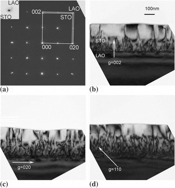
(a) Selected area electron diffraction pattern on the cross-sectional SrTiO3 (STO)/LaAlO3 (LAO) [100] interface. (b)–(d) Bright field cross-sectional images on the interface between the two-step STO thin film and the LAO substrate. The first STO layer is 10-nm thick. The images were taken using (b) g = 002, (c) g = 020, and (d)  .

III. RESULTS AND DISCUSSION
We characterized a cross-sectional sample along the [100] direction. Figure 1(a) illustrates the selected-area electron diffraction (SAED) pattern obtained from the interface between STO and LAO; it confirms that the crystallographic relationship is (001)[100]STO//(001)[100]LAO. Figures 1(b)–1(d) are bright-field (BF) images under two beam conditions with g = 002, g = 020, and  . The contrast in the STO films can be either threading dislocations or planar defects. In the BF image of a conventional single-step-grown film, similar contrast was noted owing to threading dislocations using g = 020 while it was not evident in an image using g = 002.Reference Su, Yamada, Sherman, Tagantsev, Muralt and Setter12, Reference Qin, Jia, Urban, Hao and Xi13 On the contrary, here we observed the defects using both the 020 and 200 vectors, which points to the defects other than the threading dislocations. We identified them as stacking faults from high-resolution images and plane-view images, as discussed later in the text. We noted a higher density of defects in the film’s lower part than in its upper part; evidently, strain was relaxed there, consistent with our previous reports.Reference Yamada, Astafiev, Sherman, Tagantsev, Muralt and Setter8, Reference Yamada, Astafiev, Sherman, Tagantsev, Su, Muralt and Setter9 In addition, in Figs. 1(c) and 1(d), we observed moiré fringes at the interface because of the overlapping of film and substrate.
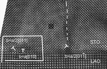
Figure 2 is a high-magnification image along the [100] zone axis. Both perfect and partial dislocations are observed at the interface; furthermore, there is an interfacial stacking fault between the partial dislocations. The relative shift in the stacking fault is 1/2a[011], consistent with an atomic shift from the oxygen atom to the neighboring strontium atom. The interfacial stacking fault might reflect the dissociation of perfect misfit dislocations during growth, as observed by others previously.Reference Qin, Jia, Urban, Hao and Xi13, Reference Lu14 Above the partial dislocations, two other stacking faults extend into the STO film. In the two-step-grown thin films, we have observed a high density of the partial dislocation and stacking faults compared with single-step-grown STO films, where most interfacial dislocations are perfect-edge dislocations with Burgers vector a<100> and with only a few stacking faults.Reference Su, Yamada, Sherman, Tagantsev, Muralt and Setter12, Reference Qin, Jia, Urban, Hao and Xi13
A cross-sectional high-resolution image on the STO/LAO interface along the [100] zone axis. Partial and perfect dislocations are marked. The stacking fault in the STO film is denoted by a dashed line.

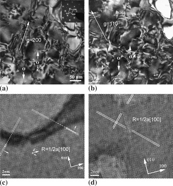
Figures 3(a) and 3(b) are plane-view BF images without substrates. The columnar-shaped grains are observed with a grain size of 50–100 nm, which is close to the distance between the stacking faults in Fig. 1. Some grain boundaries are curved, but most of them lie along the {100} planes. Inside the grains, there are only a few threading dislocations apparent in the film. However, the planar defects are not always closed; some of them are open and end at the dislocations. The corresponding SAED patterns proved that all these grains are epitaxially [001] orientated to the LAO substrate (not shown). The findings from the plane-view, bright-field images suggest that the contrasts in Figs. 1(b)–1(d) arise from the high density of the grain boundaries. To investigate the details of the boundary, we acquired high-resolution images in the plane view, as shown in Figs. 3(c) and 3(d). The former reveals an amorphous/void boundary separating two grains, whose width ranges from 0.6 to 6 nm. The upper part of the image displays a relative in-plane shift R = 1/2a[100] to the lower part. Figure 3(d) shows another type of boundary from same sample, in which the central segment is a stacking fault with in-plane shift R = 1/2a[100], whereas the other parts of boundary are voids. Altogether, we identified two kinds of grain boundaries/planar defects in terms of boundary width: a stacking fault grain boundary and a void/amorphous grain boundary. The former is a few atomic layers wide, whereas the latter is about several nanometers wide. Although similar void boundaries were reported in the (Ba, Sr)TiO3/LAO system,Reference Zhu, Chan, Wong and Hesse15 we cannot exclude the possibility of void formation during ion milling as we prepare our sample. On the other hand, amorphous-type planar defects were reported in BaTiO3 deposited on SrRuO3/SrTiO3 systems; therein, amorphization was explained by the nonstoichiometric Ti/Ba ratios in the boundary.Reference He, Vasco, Dittmann and Wang16 However, we did not detect any compositional fluctuations in our thin films. In addition, as high-resolution imaging along the [001] zone axis did not distinguish any atomic shift along this orientation, we observed only a relative in-plane shift R = 1/2a[100] or 1/2a[010], which is a projection of R = 1/2a[101] or R = 1/2a[011] observed in Fig. 2.
(a) and (b) BF plane-view images of two-step-grown STO thin films, using g vectors 020 and 110, respectively. The dislocations inside the grains are indicated by “O”. The inset of (a) shows the corresponding selected area diffraction pattern. (c) and (d) are the plane-view high-resolution images of two-step-grown STO thin films along [001].

Although partial dislocations and stacking faults with shift vectors along 1/2a<110> were observed in one-step-grown STO film, their density was low; perfect dislocation half loops were the major defects.Reference Su, Yamada, Sherman, Tagantsev, Muralt and Setter12, Reference Qin, Jia, Urban, Hao and Xi13 However, the density of the planar defects (including stacking faults and grain boundaries) was much higher in the two-step-grown film than in one-step-grown films. The grain boundary should make a major contribution to relaxing the misfit strain because it has an in-plane component of shift and a high density.Reference Yamada, Astafiev, Sherman, Tagantsev, Su, Muralt and Setter9 The different features of the two-step-grown films and conventional ones can be understood from their growth modes; we compare them next.
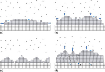
For single-step-grown films, the growth mode is that of a 2D–3D island on a layer, as illustrated in Fig. 4(a). The initial STO monolayers grow coherently on the (001) LAO substrate via a layer-by-layer process. After the film’s thickness reaches a critical value, the coherency of growth is partially broken by the appearance of dislocations that relax the misfit strain, and island nucleation occurs as illustrated in Fig. 4(b). Dislocation half-loops that form from the film’s surface are seemingly the main source for misfit dislocations.Reference Suzuki, Nishi and Fujimoto17, Reference Sun, Pan, Haeni and Schlom18
Schematic models for the growth stages of STO films. (a) and (b) One-step-grown films: (a) completely coherent growth mode of the initial stage (layer-on-layer) and (b) layer-on-island growth after the thickness exceeds the critical thickness. (c) and (d) depict two-step-grown films: (c) after annealing the first layer and (d) 3D growth of the second layer. A, B, and C indicate the interface of grain boundaries. (color online)

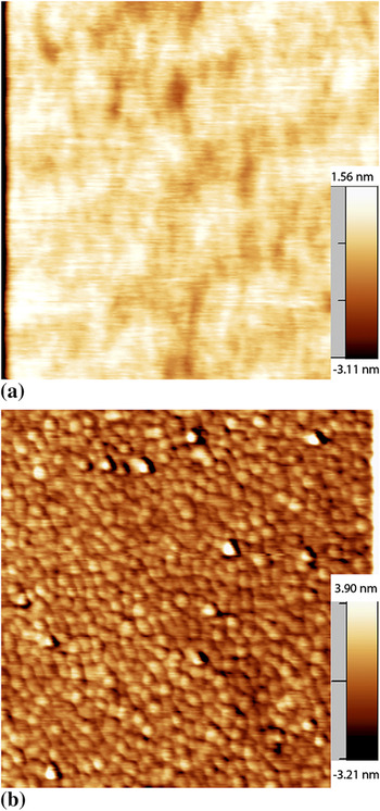
For two-step thin films, the STO FL was deposited as an amorphous film on the LAO single crystal at room temperature. It was then crystallized during annealing at 750 °C. At this temperature, the STO crystal clusters nucleate inside the amorphous STO, and most probably also on the interface of LAO, with higher nucleation intensity than during conventional deposition at high temperature. Because of boundary mismatches or diffusion barriers, these clusters may not easily merge with each other, and consequently, a poly-grain layer is formed after annealing [Fig. 4(c)]. Our assumption is supported by the surface morphology of the FL, as evidenced by AFM. Figure 5(b) is an AFM image of 10-nm FL after annealing at 750 °C wherein STO grains are apparent; surface roughness slightly increases to about 0.8–0.9 nm, from average roughness of 0.3–0.4 nm of LAO substrate [Fig. 5(a)]. In addition, the size of these STO grain is about 40–75 nm, consistent with those shown in Fig. 3. At the following stage, the growth of STO follows a 3D mode, as illustrated in Fig. 4(d), because of the existence of the multigrain surface.Reference Sanchez, Herranz, Infante, Fontcuberta, Garcia-Cuenca, Ferrater and Varela19, Reference Goh, Xu, Wang and Ong20 Grain boundaries are formed during the crystallization of FL, which are the major defects that relax the misfit strain. Growth is accompanied with the formation of stacking faults and amorphous- and void-like grain boundaries, depending on the surface mobility of the atoms relative to the deposition rate and by the substrate temperature relative to the melting temperature of the film.Reference Freund and Suresh11 During the deposition of the second layer, only a few misfit dislocations are generated by the half-loop mechanism. We note that the growth mode can be determined by the actual experimental conditions, such as oxygen partial pressure, growth temperature, deposition rate, and the surface condition of the substrate, and 3D growth have been reported for other systems.Reference He, Vasco, Dittmann and Wang16, Reference Sanchez, Herranz, Infante, Fontcuberta, Garcia-Cuenca, Ferrater and Varela19–Reference Shin, Kalinin, Borisevich, Plummer and Baddorf23
Atomic force microscope images of (a) LAO substrate before deposition and (b) the first layer of STO after annealing at 750 °C. The scan size for both images was 1 × 1 μm2. (color online)

IV. CONCLUSIONS
We investigated with TEM the microstructures of two-step-grown STO thin films deposited on LAO using PLD. In comparison to the perfect misfit dislocations and the threading dislocations found in single-step-grown films, the major defects in the two-step-grown films were partial misfit dislocations and planar defects. The annealed FL of the latter has a multigrain nature. Thereafter, the second STO layer grows on this multigrain template via 3D island growth. We suggest that grain boundaries and interfacial dislocations primarily are responsible for the relaxation of misfit strain.
ACKNOWLEDGMENTS
This work was supported in part by the Swiss National Science Foundation. N. Jiang gratefully acknowledges the financial support from National Science Foundation (NSF), DMR-0603993.