I. INTRODUCTION
Ultra low-power short-range transmitter is very challenging for its circuit design, especially when combined with the miniaturized wearable and implantable (such as intraocular signal monitoring used as post-stimulation biofeedback of visual prosthesis) devices for sensor networks. The transmitter, as such, can be implemented in the conventional I/Q modulators [Reference Lee1], which results in high circuit complexity, large area, and considerable power dissipation. binary frequency shift keying (BFSK) modulation utilizing fractional phase-locked loop (PLL) with Sigma-Delta Modulator provides a viable way of reducing area and power consumption [Reference Khalil2]. Its data rate is, however, compromised by the PLL loop bandwidth. As an alternative, BFSK modulation utilizing open-loop frequency synthesizer has a unique feature that upon phase locking, the loop of the PLL involved can be broken, thus achieving PLL-loop-bandwidth-independent modulation with high data rate. The open-loop modulation scheme also allows minimization to power as it could disable not only the frequency synthesizer from it (except the voltage-controlled oscillator (VCO) involved), but also the potential downstream circuits such as the power amplifier when the loop is formed [Reference Karam3]. We showcase here a BFSK modulator, a 1.5 V 400 MHz 1 Mbps 0.18 µm complementary mental-oxide semiconductor (CMOS) design achieving only 3.1 mW, typifying such open-loop circuitry.
II. DESIGN
A) Architecture
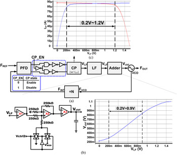
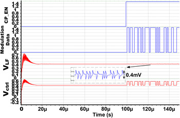
The architecture of the analog adder technique (AAT)-based BFSK modulator is shown in Fig. 1(a). It has two unique circuits termed CP_EN and Adder. The CP_EN circuit renders the modulator functional for two operating modes: the “Close-loop Frequency Synthesis (CFS)” mode and the “Open-loop BFSK Modulation (OBM)” mode, which can be selected by the control input CP_EN. When CP_EN is logic LOW, modulation is OFF and the modulator behaves as a frequency synthesizer (the CFS mode). By contrast, the CP circuit is disconnected from the supply and referred ground to break the loop for modulation when CP_EN is logic HIGH (the OBM mode). Entering the OBM mode, modulation can be performed by utilizing V ctrl2 as a binary digit and V MOD . To reduce the VCO frequency drift caused by the floating V LF nature of the open-loop schemes, an Adder circuit is first introduced to treat the problem. A1 functions as a buffer to ensure that V LF is properly isolated. Simulation results, shown in Fig. 2, provide evidence of how V LF can be protected from disturbance of modulation (only 0.4 mV voltage variation). The VCO circuit determines the input and output linear ranges of the Adder circuit. In this work, V ctrl is set from 0.28 to 0.83 V to achieve a KVCO of 18.4 MHz/V, thus obtaining an input range of 0.2–0.9 V for Adder and its A1 (Fig. 1(b)). The output range of the CP circuit is selected as 0.2–1.2 V with a match between its current source and the current sink (ICP is about 90 µA), which can be seen from the results shown in Fig. 1(c).
Proposed BFSK modulation architecture and its block diagrams.

Evidence showing that V LF can be protected from disturbance of modulation.

The proposed architecture, which is based on frequency synthesis, features three advantages. The first is its low-power consumption at in open-loop mode. In the open-loop operation, the PFD, CP, and Divider circuits stay asleep, thereby reducing the overall power dissipation. The second is that its open-loop architecture possesses low design complexity. The third is that the data rate does not have to be limited to the loop bandwidth. V ctrl2 represents the binary data stream used to enable modulation. V ctrl can be decided by V ctrl2 and its voltage will be either V LF or V LF + V MOD , where V MOD is a voltage used to produce frequency shifting. The BFSK output F OUT is the sum of the frequency shift, the product of V MOD and the VCO gain, and the quiescent frequency of the oscillator.
The proposed analog adder between the LPF and the VCO should be simple. However, the adder circuit results in a pole. In the time domain, the pole causes a group delay (loading effect). If the delay is too long, the locking time of the PLL will be affected, resulting in instability. Nevertheless, the pole should not affect the stability of the system at open-loop operation because only local feedback instability is possible in PLL open-loop and it can be easily avoided using e.g. miller feedback in the operational amplifier (op amp). We added the circuits A1, A2, and A3 into the analog adder to minimize the loading effect. A3 can be used to isolate Adder from VCO in order to reject the noise stemming from Adder that affects the oscillation frequency. The unity-gain bandwidths of A1, A2, and A3 should be 10 times higher than the loop bandwidth of the system.
B) Circuits
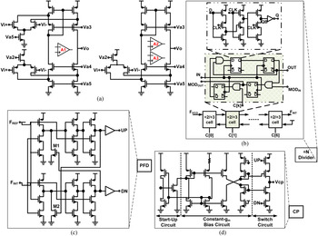
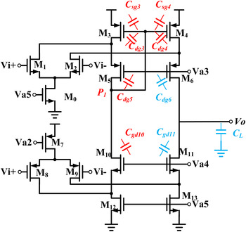
Implementations of A1, A2, and A3 are shown in Fig. 3(a). A complementary folded-cascode op amp is chosen for A1 to accommodate the input linear range of 0.2–0.9 V as compared with A2 requiring only the P-type mental-oxide semiconductor (PMOS) input pair. A1 has been designed in the unity gain structure as the input buffer. A2 consists of the addition stage and unity gain buffer stage. Because they exist between the LPF and VCO, they do not need wide unity-gain bandwidth, due to the lower signal frequency at the LPF output. As a result, it is sufficient that they are designed in first-order amplifier structure. The first-order amplifier design gets rid of the instability. Pole positions can be illustrated with Fig. 4. For our design, the output of the amplifier V o possesses largest capacitive load. This means C L ≫ C dg6, C gd11 and the dominant pole will occur at the node V o . The angular frequency of dominant pole can be written as
 $$\omega _{Vo} = \displaystyle{1 \over {R_{out} (C_L + Cdg_6 + Cgd_{11} )}},$$
where,
 $$\eqalign{& Rout = Rop//Ron \cr & Ron \approx gm_{11} ro_{11} (ro_{13} //ro_9 ) \cr & Rop \approx gm_6 ro_6 (ro_4 //ro_2 ).} $$
Schematics of the circuits constructing the open-loop frequency synthesizer.

Circuit schematic of A1 showing capacitive loads.

The node P 1 should be carefully checked, due to its significant parasitic capacitance. The angular frequency of pole at the node P 1 can be written as
 $$\omega _{P1} = \displaystyle{1 \over {R_{out} (Csg_3 + Cdg_3 + Csg_4 + Cdg_4 + Cdg_5 + Cgd_{10} )}}.$$
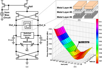
As a result, care must be taken to properly size the transistors to keep ω P1 far away from ω Vo in order to have sufficient phase margin. Note that the Adder circuit has a gain of approximately 1 in practice. The unity gain bandwidths (UGBWs) of A1, A2, and A3 should be respectively, higher than the PLL loop bandwidth (80 kHz in this work) and the maximum data rate (1 Mbps in this work) as far as their designs are concerned. Here, the UGBWs are 12.8 and 10.7 MHz for A1 and A2 (A3), respectively. Thanks to the bandwidths (≫80 kHz loop bandwidth of the system), the proposed analog adder does not affect the open-loop frequency response of system. A divide-by-157 dual-modulus prescaler (Fig. 3(b)) is employed to have a F OUT of 401.92 MHz at F REF = 2.56 MHz (chosen for a neural recording application according to [Reference Chen4]). The dynamic PFD circuit shown in Fig. 3(c) has M1 and M2 to avoid erroneous operation for UP and DN. The CP circuit shown in Fig. 3(d) is with switching-charge-injection-immune characteristic on VCP. VCO dominates the power consumption and phase noise (PN) of the synthesizer. In view of this, the VCO is implemented in the structure shown in Fig. 5(a) wherein it is with a 3-bit switched capacitor array and its inductor quality factor (Q) is improved by a selective metal parallel shunting technique shown in Fig. 5(b) [Reference Wu5] to achieve low-PN (Q is improved from 6 to 14.5 at about 400 MHz). To make better compromise between low-PN and low-power consumption, the plot shown in Fig. 5(c) has been made, thereby optimizing the VCO at a supply (VDD) of 1.5 V and a tail current (Itail) of 1 mA.
Circuit of VCO with 3-bit switched capacitor array and the Q-improved inductor.

III. EXPERIMENTAL RESULTS
To understand, if our design is fully functional, we have implemented different measurement switches in the circuits. In the VCO, we used a spectrum analyzer (Agilent 4395A) to measure its spectrum and output power. The time domain signal of the synthesizer was monitored by an oscilloscope (Agilent DSO9064A). Their PNs were obtained by a signal source analyzer (Agilent E5052B). In the proposed analog adder, the same oscilloscope was used to record its input–output linearity. The modulation data stream was generated from an arbitrary waveform generator (Agilent N6032A). In the layout of the printed circuit board of fabricated chip, we allocated spaces and pins to decoupling capacitors for supply voltage ripple reduction. In addition, we have also allocated spaces and pins to choke inductors used to block higher-frequency signals. The inductors were placed between the external power supply and the fabricated chip to generate the high-quality internal DC supply voltage.
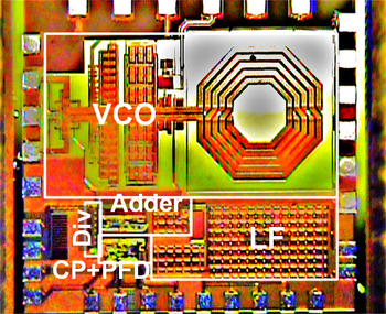
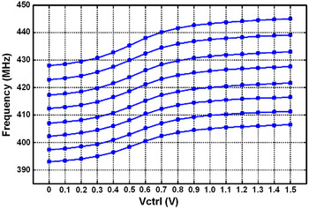
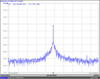
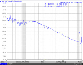
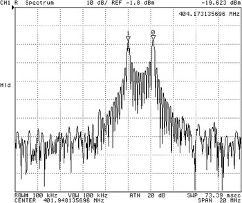
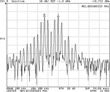
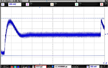
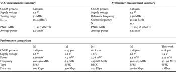
Figure 6 shows the prototype whose die size is 1.5 × 1.33 mm2. Measured results illustrating the operation of the proposed modulator are shown in Figs 7–12. Figure 7 shows the VCO tuning range wherein it is tunable from 393 to 445 MHz at KVCO of 18.4 MHz/V. The VCO circuit has a measured central frequency of 402 MHz. The measured VCO PN is −111.7 dBc (at 1 MHz offset). Figure 8 shows that the synthesizer can be successfully locked at the VCO central frequency. Figure 9 shows the PN of the synthesizer. In comparison with the integrated VCO, the synthesizer has better PN than that of the VCO circuit within the PLL loop bandwidth (80 kHz). Figures 10 and 11 show the proposed design working at the OBM mode wherein the (b) and (c) demonstrate a data rate of 200 Kbps and a data rate of 1 Mbps, respectively. It can be discovered that, at higher data rate, the harmonic distortion increases. Higher data rate means higher input frequency. It means higher slew rate is required, resulting in higher UGBW required. As a result, insufficient UGBW or slew rate causes increased harmonic distortion at higher data rate. Figure 12 shows a <30 µs lock for the synthesizer. The average bit error rate of the modulator is about 0.1% at 200 Kbps with a pseudo-random bit pattern where a power supply variation of 10% was imposed in the measurement. The measurement summary results and the comparison of the performance metrics with the state-of-the-art are given in Table 1. The proposed modulator is fully functional for its two operating modes, suggesting a promising solution for the wireless systems.
Die photo of proposed AAT-based modulator.

Measured VCO tuning range.

Measured synthesizer spectrum.

Measured results of the synthesizer (PN).

Measured spectrum of BFSK modulation (200 Kbps).

Measured spectrum of BFSK modulation (1 Mbps).

Measured waveform demonstrating a <30 µs locking time of the synthesizer.

Measurement summary results and the comparison of the performance metrics with the state-of-the-art.

The constant-gm bias circuit used in the proposed modulator is chosen for simplicity. However, it suffers from bad power supply rejection capability (line sensitivity). In a general top-down design of system on chip the final layout should contain a regulator specifically developed for automatically maintaining several constant voltage levels and providing a regulated power supply voltage. It is used in the circuits, which includes the proposed design with the constant-gm bias circuit, requiring sufficient power supply rejection capability. With regards to the performance affected by the line sensitivity, power supply variation can produce an unwanted component of output frequency change. The sensitivity of the VCO to power supply variation results in a fraction of the wanted gain of the error voltage from the phase detector into an output frequency. For a high-gain VCO, the effect becomes larger, and the noise contribution from the supply becomes more remarkable. Motivated by this, a measurement has been conducted by applying tunable DC bias to the fabricated chip and varying the supply voltage, followed by measuring the frequency change. The sensitivity (gain variation) of about 3.7 MHz/V is obtained by means of the ratio of frequency change to voltage change. This means power supply rejection ratio still has room to improve.
For the CP, the current offset between up and down stages will affect the V cp , which directly affects the V ctrl of VCO. This results in oscillation frequency deviation. To avoid the offset, we have designed the circuit to have a V cp wider than the input range of Adder (0.2–0.9 V). Normally, operation of the system falls within the input range of Adder. Frequency deviation occurs if offset happens. As suggested, a compensation mechanism is required to carry out offset cancellation. Nevertheless, the current IC is mainly for the purpose proving that our design is functional in terms of the proposed open-loop modulation. Efforts are underway to include a compensation scheme in the next version.
IV. CONCLUSION
Transmitting sensed physiological data in a wireless way with a low-power, light-weight, and portable device is essential for new-generation bio-implants, healthcare delivery systems, and information and communications technology (ICT)-based service of diagnosis and treatment. Our brand new 1.5 V 400 MHz 1 Mbps BFSK Modulator achieving 3.1 mW suggests that it provides a promising tool whenever applied to the applications. Our work is ideal for biomedical sensor network systems including distributed wearable body area network.
ACKNOWLEDGEMENTS
The authors would like to thank Chip Implementation Center, Taiwan. This study was supported by National Science Council, Taiwan, and Ministry of Science and Technology, Taiwan, under Grants MOST 104-2221-E-182-044 – and MOST 104-2815-C-182-052-E. It is also supported in part by the Chang Gung University and Chang Gung Memorial Hospital under Contracts UERPD2E0031 and CMRPD2E0021.
STATEMENT OF INTEREST
The authors declare that there is no conflict of interests in this paper with any trademark or software mentioned.
 Kai-Wen Yao was born in Pingtung, Taiwan, in 1981. He received his B.E. degree in Biomedical Engineering from Chung Yuan Christian University in 2004, the M.S. degree in Biomedical Engineering from the Division of Bioelectronics, National Yang-Ming University, Taipei, Taiwan, in 2006, and the Ph.D. degree in Electrical Engineering from National Central University, Jhongli, Taiwan, in 2015. Dr., Yao's research interests include biosignal measurement systems and front-end circuitries for neural recording systems.
 Cihun-Siyong Alex Gong has been involved in biomedical circuits and systems since he started his M.S. program. He received his B.S. degree in Civil Engineering, the M.S. degree in Biomedical Engineering, and the Ph.D. degree in Electrical Engineering, in 2002, 2005, and 2008, respectively. In 2009, he joined the Industrial Technology Research Institute, Hsinchu, Taiwan, as one of the Research and Development Staff Members and has become an IEEE Member since then. He held Adjunct Assistant Professor position at National Taiwan Normal University, Taipei, Taiwan, and National United University, Miaoli, Taiwan, in 2012 and 2013, respectively. He joined the Department of Electrical Engineering, School of Electrical and Computer Engineering, College of Engineering, Chang Gung University, Taoyuan, Taiwan, in 2013, where he is presently an Assistant Professor and with the Portable Energy System Group, Green Technology Research Center. His research interests are in electronics for medicine and healthcare, including interfacing-associated solid-state circuits and their physiological issues. He chaired the sessions on Advanced Circuit and System on Green and Biomedical Applications, Information and Communication Technology for Translational Medicine and Green Applications, and RF and Wireless for the IEEE ISCE 2013, IEEE ICCE-TW 2014, IEEE ICCE-TW 2015, and IEEE ICCE 2015, respectively. Dr., Gong has been Technical Program Committee member of the above mentioned conferences including also the IEEE GCCE 2015 and IEEE ICCE 2016. He has been Technical Program Co-chair of the 2016 Symposium on Engineering, Medicine and Biology Applications (SEMBA), Taiwan, and Publicity Chair of the IEEE ICCE-TW 2015. Alex was a recipient of the 2004 Domestic Annual Symposium on Biomedical Engineering Excellent Paper Awards, the 2005 NYMU Honours Student Awards in memory of the Yin, Syun-Ruo, the 2008 NCU Outstanding Graduate Student Awards, the Best Student Paper Contest Awards in the 2008 IEEE International Conference on Electron Devices and Solid-State Circuits, the 2009 Best Design Awards of the CIC, Taiwan, the 2009 Taipei International Invention Show and Technomart Gold Medal Awards, the 2012 Best Paper Awards of the CCL Technical Journal, the Honorable Mention Awards at the 2013 Biomedical Engineering Symposium on 4B, Taiwan, and the Honorable Mention Awards at the IEEE ICCE-TW 2014. Prof. Gong founded MIX studio, Taiwan, and was working for Merry Monarc(h) studio, Taiwan, prior to his academic career.
 Yu-Ting Hsueh received his M.S. degree in Electrical Engineering from National Central University, Taiwan, in 2011. He is presently a Senior IC Design Engineer.
 Yu Lin Tsou received his M.S. degree in Electrical Engineering from National Central University, Zhongli, Taiwan, in 2004 and 2006, respectively. He earned his Ph.D. degree in Communication Engineering at National Chiao Tung University, Hsinchu, in 2015, with a focus on ultra low-power RF system for wireless sensor network applications. He was with the Department of Low Power Mixed Signal, Industrial Technology Research Institute, Hsinchu, Taiwan, where he was involved in designing ultra low-power analog and RF ICs. Dr., Tsou is presently working for the MediaTek Inc.
 Muh-Tian Shiue was born in Taichung, Taiwan, in 1963. He received his B.S. degree in Industry Education from National Taiwan Normal University in 1986, the M.S. degree in Control Engineering from National Chiao Tung University, Hsinchu, Taiwan, in 1988, and the Ph.D. degree in Electrical Engineering from National Central University, Jhongli, Taiwan, in 1998. From 1988 to 1996, Dr., Shiue was with the Transmission Technology Laboratory of Telecommunication Laboratories, Ministry of Transportation Communications, Taiwan, where he was involved in the digital subscriber loop technologies. From 1998 to 2000, he was with the Computer and Communications Research Laboratories, Industrial Technology Research Institute, Hsinchu, Taiwan, where he was involved in the development of ADSL chip-set. He joined IC Plus Corp. corresponding to the digital baseband chip design for ADSL transceiver in 2000. From 2001 to 2003, he was the CTO of Trendchip Technologies Corp. Presently he is with the Department of Electrical Engineering, National Central University, where he is an Associate Professor. Prof. Shiue's research interests include local access technologies, digital subscriber loop technologies, wireless communication systems, biomedical engineering, digital signal processing, VLSI techniques, and control systems.
 Jian-Chiun Liou received the Ph.D. degree from Institute of NanoEngineering and MicroSystems, National Tsing Hua University, Taiwan. Dr., Liou is presently an Assistant Professor with National Kaohsiung University of Applied Sciences. Prof. Liou focuses on the research field of Nano Microelectromechanical Systems integration with ASIC.
 Yih-Shiou Hwang is presently a Medical Doctor with Department of Ophthalmology, Chang Gung Memorial Hospital, Taiwan. Dr., Hwang is also an Assistant Professor of Graduate Institute of Clinical Medical Sciences, Chang Gung University, Taiwan.