I. INTRODUCTION
Ion irradiation of materials is known to introduce defects and affect phase transformation by driving the system toward nonequilibrium.Reference Varichenko, Zaitsev, Kazutchits, Chelyadinskii, Penina, Martinovich, Latushko and Fahrner1–Reference Utsunomiya, Wang, Yudintsev and Ewing7 Technically, it has exciting potential for surface modification and doping of the thin films. In addition to implantation, ion irradiation enhances the diffusion processes through the creation of defects in the material being irradiated. Therefore, depending upon the free energy and chemical potential landscapes, it can promote either mixing or phase separation processes. A significant amount of work has already been carried out using inert gas ion irradiation and implantation, using Xe ionsReference Templier, Gaboriaud and Garem8–Reference Mitsuishi, Song, Furuya, Birtcher, Allen and Donnelly12 in particular. The implanted Xe bubbles become crystalline at small sizes. If embedded in fcc materials such as aluminum, the structure of crystalline Xe is fcc and exhibits an epitaxial cube on cube relation with the matrix.Reference Templier, Gaboriaud and Garem8 The observed shape of the crystalline Xe is cuboctahedral,Reference Allen, Birtcher, Donnelly, Song, Mitsuishi, Furuya and Dahmen9 conforming to the expected equilibrium shape.
Recently, coatings of materials showing superior mechanical properties, high temperature stability, excellent corrosion resistance, and good thermal conductivity have attracted great research interest for various applications in advanced nuclear reactors.Reference Wang, Araoujo, Swadener, Wang, Zhang, Fu and Cagin13–Reference Uglov, Rusalski, Zlotski, Sevriuk, Abadias, Kislitsin, Kadyrzhanov, Gorlachev and Dub15 The intermetallic compound Ti5Si3 shows such excellent properties, and hence coatings of this intermetallic composition have the potential to find application in nuclear reactors. Therefore, it is important to study the effect of ion irradiation on the microstructure and phase evolution in these thin film coatings, since the properties of the coating depend on its microstructure and constituent phases as well as the distribution of phase and the implanted species, if any.
We report in this paper the effect of irradiation of Xe ions on both amorphous and crystalline films of Ti-Si alloy close to the composition of intermetallic Ti5Si3 compound. We show that ion irradiation not only promotes a composite of nanocrystalline and amorphous phases for both types of films, but also yields embedded Xe nanoparticles having an amorphous structure. Our results suggest that Xe irradiation leads to similar microstructures in both amorphous and crystallized films of Ti5Si3 alloy. However, the nature of interaction of the Xe ion beam with the samples is different for the two cases. In case of the amorphous Ti-Si film, the ion-irradiation promotes partial nanocrystallization of the amorphous phase yielding a metastable phase having fcc structure. On the other hand, in the case of the crystalline film, ion irradiation tends to amorphize the sample with the dissolution of the equilibrium Ti5Si3 phase and simultaneous formation of metastable fcc nanocrystals. Thus, our results suggest that under driven conditions (due to ion irradiation) partial nanocrystallization of the Ti-Si film stabilizes the amorphous phase. The most significant of the present results, however, is the formation of nanosized implanted Xe with an amorphous structure.
II. EXPERIMENTAL
Amorphous thin films of about 50 nm thickness and a composition close to Ti62.5Si37.5 were deposited at room temperature on NaCl substrates by laser ablation of a target of Ti5Si3 intermetallic compound. The details of the deposition experiments have already been described in a previous publication.Reference Bysakh, Das and Chattopadhyay16 The films on NaCl substrates were scratched with a diamond pen into square fragmented areas of about 3 mm size each. These film fragments were floated in distilled water by slowly immersing the NaCl substrate and allowing it to dissolve in water. The floating film fragments were subsequently collected on 300 mesh TEM grids. The collected TEM samples were washed repeatedly in distilled water to ensure complete removal of any residual NaCl. Some of the deposited films on TEM grids were heated to 800 °C inside the TEM column to induce crystallization under the high vacuum condition. Both the as-received and crystallized films were irradiated with 100 keV Xe ion beam using a custom-built ion-irradiation facility attached to the high-voltage high-resolution transmission electron microscope (TEM) JEOL ARM1000 at the Nanomaterials Laboratory, National Institute for Materials Science, Tsukuba, Japan. The irradiation experiments were carried out in situ inside the TEM column for 30 min with an ion beam induced current of about 8 × 10⁻⁹ A to obtain an ion fluence of about 1016 ion·cm−2. A custom-built Faraday cup detector of 2.5 mm diameter mounted in a TEM specimen holder was used to measure the ion current on the actual specimen to be irradiated. Following the irradiation, the structural characterization of samples was carried out in the same microscope using its high resolution imaging capability. Energy dispersive spectroscopic composition analysis of the films was carried out using the analyzer available in the same microscope. Further composition analyses of the samples were carried out using a JEOL JEM 2010F TEM (JEOL Ltd., Tokyo, Japan) equipped with a Thermo Noran EDS analyzer (Thermo Noran, Middleton WI). Nanoprobe EDS composition mapping was obtained by using a Tecnai G2 30ST analytical scanning transmission microscope (FEI Company, Eindhoven, The Netherlands) equipped with LaB6 thermionic electron source and EDS manufactured by EDAX (EDAX Inc., Mahwah NJ).
III. RESULTS
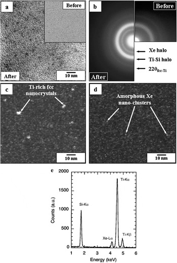
In the inset of Fig. 1(a), we present a typical bright field TEM micrograph of the as deposited film. No features other than the granular contrast typical of amorphous films can be observed. The bright field TEM image of the amorphous film after 100 keV Xe+ ion irradiation is shown in Fig. 1(a), which reveals a distribution of fine nanocrystals in an amorphous matrix. The selected area diffraction patterns (SAD) obtained from the deposited films before and after irradiation are compared in Fig. 1(b). The SAD of the as-deposited film shows a prominent diffuse halo indicating the amorphous nature of the film. In contrast, the SAD pattern from the irradiated film reveals two additional features. The first one is an additional diffuse halo which could be seen at a low angle. The scattering vector Q, corresponding to the maximum of the extra halo ring was determined from the measurement of the diameter, D, of halo maxima and applying the formula:

(a) The BF TEM micrograph of the Xe-ion irradiated Ti62.5Si37.5 film revealing dispersion of nanosized crystalline particles in the amorphous matrix. Inset shows the microstructure of the film before irradiation. (b) The SAD pattern of the film before irradiation (right) and after irradiation (left). The indexing of the additional rings after irradiation is indicated. (c) DF micrograph using the 220 fcc ring. (d) DF using the additional diffuse halo at low angle due to Xe. Note diffuse intensity of the fine domains. (e) Representative EDS spectrum obtained from the film showing the characteristic XeLα peak at an energy value of 4.15 keV.

where d is the real space distance corresponding to the scattering vector, L is the camera length used in the TEM to form the electron diffraction pattern, λ is the wavelength of the beam electron, and D is the measured diameter of the halo maximum.
The magnitude of the scattering vector thus obtained was 18.85 nm−1. The significance of this value of the scattering vector for the extra-halo maximum will be discussed in Section IV.
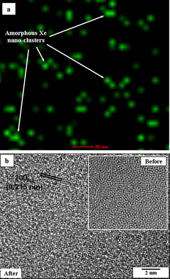
The second additional feature in the electron diffraction pattern of the irradiated film is a sharper outer ring typical of a crystalline phase. This ring can be indexed as a 220 reflection of a previously reported metastable fcc phase of Ti-Si alloys.Reference Bysakh, Das and Chattopadhyay16 Both the 111 and 200 reflections of this phase merge with the halo of the amorphous Ti-Si phase, as can be understood from the crystallographic data listed in Table I and Table II. A dark field image of a portion of this ring indicates the presence of nanocrystals [Fig. 1(c)]. The dark field image taken from the additional low angle diffuse halo reveals uniformly distributed diffracting nanodomains with relatively weak intensities [Fig. 1(d)]. Energy-dispersive x-ray analysis available with the microscope indicated the presence of about 5 at.% Xe in the irradiated sample. The experimental EDS spectrum is presented in Fig. 1(e), which clearly shows the characteristic XeLα peak at an energy value of 4.15 keV in agreement with earlier work.Reference Michell, Donnelly, Glanvill, Miller and Rossouw17 It was possible to obtain the distribution of the Xe by elemental mapping using EDS composition analyzer with nanoprobe electron beam scanned over the thin film sample in the TEM. Figure 2 shows the result of the mapping revealing finely dispersed nanodomains containing implanted Xe. Note that the nanoprobe EDS mapping image only shows the locations of nanodomains of high Xe concentrations in the implanted film sample, and may not represent the exact size or shape of Xe-rich nanodomains. This is primarily because the EDS mapping image was obtained by scanning an electron beam of about 5 nm probe size available with our TEM equipped with thermionic LaB6 electron gun. In addition, since the 3D information within the specimen thickness is being represented in a 2D image, some of the Xe nanoclusters on top of the other may appear as a cluster of size larger than the actual. Nevertheless, the observed domains are at similar locations to that observed in the dark field image of Fig. 1(d). High resolution imaging of the irradiated film, however, only revealed crystalline domains of fcc Ti(Si) phase [Fig. 2(c)]. The Xe clusters could not be identified separately in the amorphous matrix while high-resolution imaging of the matrix yields typical granular contrast associated with an amorphous structure.
(a) Nanoprobe EDS mapping of implanted Xe domains in the irradiated sample. (b) High resolution TEM image of the irradiated sample revealing crystalline domains of fcc metastable phase. Inset shows the as deposited amorphous film with granular contrast for comparison.

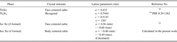
List of crystal structures and lattice parameters of fcc Ti(Si), Ti5Si3, fcc Xe, bcc Xe, and real-space distances corresponding to the diffraction halo maxima from amorphous Ti(Si) and amorphous Xe in the as implanted and heat treated Ti62.5Si37.5 films.

List of the interplanar spacings (d-spacing) corresponding to the strong diffraction rings from fcc Ti(Si), Ti5Si3, fcc Xe, bcc Xe and real space distance corresponding to the diffraction halo maxima from amorphous Xe in the as implanted and heat treated Ti62.5Si37.5 films.

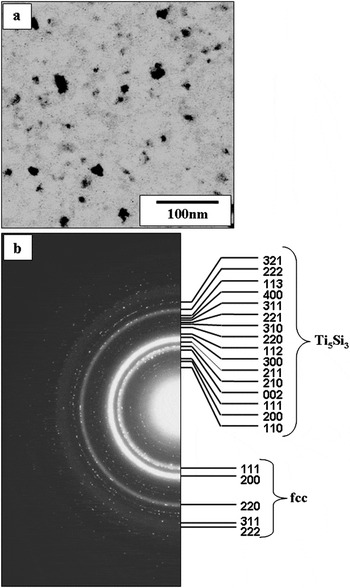
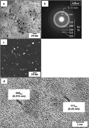
In a second set of experiments, we heated the as deposited amorphous films inside the microscope column. We observed partial crystallization of the films with the formation of fine Ti5Si3 crystals having a hexagonal crystal structure (a = 0.7444 nm, c = 0.5143 nm) in addition to the fcc phase when the sample was heated above 700 °C. A typical bright field microstructure of a sample heated at 800 °C for 1 h is shown in Fig. 3(a) revealing these crystallites. The corresponding SAD pattern is shown in Fig. 3(b). Note the spotty crystalline rings of the Ti5Si3 phase. The indexing of the pattern is given in the right half of the pattern. The same sample is again irradiated with Xe inside the microscope under the identical condition as used for the as deposited case. Figure 4(a) shows the bright field micrograph while the selected area diffraction pattern with indexing is shown in Fig. 4(b). The diffraction pattern is marked by the disappearance of the Ti5Si3 phase and the retention of the metastable fcc Ti(Si) phase. Figure 4(c) shows a dark field TEM image using a portion of the crystalline fcc ring. A high resolution image of the same area showing crystallites of fcc phase in an amorphous matrix is presented in Fig. 4(d). The diffraction pattern [Fig. 4(b)] also reveals a diffuse halo, characteristic of the implanted amorphous Xe, in addition to the diffuse intensity from the residual Ti(Si) amorphous regions still existing in the film. The crystal structures and lattice parameter values of the crystalline phases fcc-Ti(Si), h-Ti5Si3, fcc-Xe, and bcc-Xe are listed in Table I. The interplanar spacing values corresponding to the strong reflections of these crystalline phases, along with the real-space distances corresponding to the maxima of diffraction halos from amorphous Xe and amorphous Ti-Si, are listed in Table II.
(a) A bright field TEM micrograph of the laser ablation deposited Ti-Si thin film sample after heat treatment at 800 °C for 1 h. (b) SAD pattern of the above. The indexing of the rings is given in the right half.

Nanostructure of crystallized Ti62.5Si37.5 film irradiated with 100 kV Xe ion beam. (a) Bright-field image showing the presence of fine nanocrystals (≤10 nm) and the larger Ti5Si3 nanocrystals (20–50 nm) are absent. (b) SADP of the irradiated film showing the Xe halo, the Ti-Si halo, and the sharp fcc-Ti(Si) rings. Note the disappearance of Ti5Si3 spotty rings. (c) Dark field image formed with the first two sharp rings illuminates the fcc nanocrystals. (d) HREM image of the irradiated film showing the presence of mainly fine fcc nanocrystals and amorphous matrix.

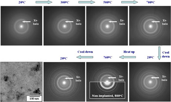
To establish whether the structure of implanted amorphous Xe changes with heating, the as deposited sample implanted with Xe was heated in the microscope. The evolution of the diffraction patterns during heating up to 760 °C is presented in Fig. 5. The diffuse Xe peak remains unaltered while spotty rings of Ti5Si3 reappear at higher temperatures, indicating the stability of amorphous Xe domains.
Amorphous xenon remains implanted even after heating the irradiated sample up to 760 °C, when significant diffusion allows Ti5Si3 nanocrystals to grow up to a few tens of nanometers. Neither heating nor subsequent cooling to room temperature result in crystallization of implanted Xe, hence there was no obvious sharpening of the Xe halo. The bright field TEM image at the end of the experiment shows no observable Xe bubble formation.

IV. DISCUSSION
The results presented above provide us an insight into the effect of 100 keV Xe ion irradiation on the evolution of metastable nanostructure in the intermetallic film. The amorphous nature of the as deposited film due to the drastic quenching involved in the pulsed laser deposition process and the evolution of film nanostructure consisting of fine fcc and coarser Ti5Si3 nanocrystals during heating up to 800 °C have already been dealt with in an earlier publication.Reference Bysakh, Das and Chattopadhyay16 The EDS spectra of the irradiated films show a small extra peak due to XeLα as direct evidence of the presence of a significant amount of Xe implanted in the film and quantified to be about 5 at.%. The EDS analyses of both the amorphous and nanocrystallized films before and after irradiation indicate that the binary Ti-Si composition of the films did not change significantly during irradiation except for the implantation of the Xe atoms.
As indicated in Sec. III, the broad and smooth nature of the extra halo in the electron diffraction pattern from the xenon implanted film indicates the noncrystalline nature of the implanted Xe. The maximum of the extra halo ring occurred at a scattering vector (Q = 4 πsinθ/λ) value of 18.85 nm−1. This value corresponds to a real space distance of ~0.333 nm. It is important to note that a similar Q value (18.7 nm−1) was reported in an earlier work on fluid Xe implanted in amorphous Si.Reference Zontone, D’Acapito, Faraci and Pennisi18 A greater scattering vector for amorphous Xe in our case means a smaller real-space distance (~0.333 nm) between the adjacent Xe atoms compared to the distance of ~0.336 nm calculated from the Q value reported for fluid Xe implanted in Si. This in turn means a slightly greater density of the xenon in our study and therefore hints at the possibility that the noncrystalline xenon nanoclusters observed in our case are under a slightly higher pressure compared to the implanted fluid Xe reported in the literature. We note here that otherwise, there is little difference between the terms of fluid Xe used in an earlier reference and amorphous Xe used by us.
The dark field images formed by using the extra Xe halo ring showed a uniform distribution of weakly illuminated ultrafine nanodomains of about one nanometer size. Therefore, our results suggest the formation of small Xe-Xe clusters, with short range order similar to that of the fluid Xe implanted in Si.Reference Zontone, D’Acapito, Faraci and Pennisi18, Reference Faraci, Pennisi and Zontone19 Note further that larger (5–20 nm size) Xe bubbles, both crystalline and amorphous, have already been observed in other implanted crystalline materials.Reference Michell, Donnelly, Glanvill, Miller and Rossouw17, Reference Zontone, D’Acapito, Faraci and Pennisi18 In our case, the total absence of such embedded Xe nanocrystals or any larger bubbles suggest noncoalescence of the implanted Xe atoms. This is most likely due to the constrained atomic movement or diffusion at room temperature owing to the high melting point (2130 °C) of the material of our film. It may also be worth mentioning that several publications based on molecular dynamics simulation of ordering and phase transition of implanted Xe predicted a bcc structureReference Donnelly, Birtcher, Allen, Morrison, Furuya, Song, Mitsuishi and Dahmen20 for a tiny volume of ~8 nm3 and fcc to bcc phase transitionReference Desgranges and Delhommelle21, Reference Belonoshko, Lebacq, Ahuja and Johansson22 under extremely high pressure. However, the electron diffraction evidence in our case of nanometer size Xe clusters suggests only amorphous xenon and the halo-ring maxima could not be correlated to either fcc or bcc structure. Therefore, our findings suggest that the implanted nanometer size Xe clusters have neither undergone structural ordering nor are they under the high pressure necessary for their crystallization into either bcc or fcc structure. Our results indicate that the effect of Xe irradiation on Ti-Si intermetallic films has a close similarity to that observed for Si.Reference Zontone, D’Acapito, Faraci and Pennisi18, Reference Barberi, Landers, de Oliviera, Alvarez and Marques23
The evolution of the nanocrystalline fcc Ti(Si)-solid solution phase in both amorphous and nanocrystallized films during ion irradiation as well as during heating the amorphous phase, indicates that this phase certainly has a competitive driving force for nucleation. The nucleation of the fine fcc-Ti(Si) nanocrystals due to irradiation can be explained as the result of two opposing processes taking place during ion irradiation. On one hand, the atomic shuffling due to the bombardments of energetic heavy ions induces atomic movements similar to those during thermal annealing and hence helps the atomic species in overcoming the nucleation barrier for the kinetically favored crystalline phase. On the other hand, the disordering effect of bombardments tends to induce randomness into the atomic arrangements in the irradiated material as is manifested in the dissolution of the large Ti5Si3 nanocrystals into the amorphous matrix. The competition between these two opposing processes has resulted in the nucleation of tiny fcc-Ti(Si) nanocrystals in an amorphous matrix under the influence of high-energy xenon ion irradiation. It may be worth mentioning that our case is similar to the case of ion irradiation of NiAl2 reported in the literature. However, in our case, the implanted Xe remains in the form of noncrystalline nanoclusters, clearly indicating the role of the embedding matrix in the crystallization process of implanted Xe. The amorphous Ti-Si matrix does not provide a heterogeneous site for the fcc Xe crystal nucleation, thus constraining it to have a noncrystalline structure.
Reheating the Xe-implanted film composed of fcc-Ti(Si) and an amorphous matrix results in the reappearance of the larger Ti5Si3 nanocrystals. However, the implanted amorphous Xe is retained in the form of noncrystalline nanoclusters. According to our experimental results, and as discussed above, the regrown Ti5Si3 nanocrystals are expected to disappear again upon Xe ion irradiation.
V. CONCLUSIONS
(i) Xe was implanted into both amorphous and nanocrystallized pulsed laser deposited Ti-Si films without a change in relative amounts of Ti and Si.
(ii) The implanted Xe exists in an amorphous state in the Ti-Si films in the form of nanoclusters.
(iii) The fine nanocrystalline fcc-Ti(Si) phase has a nucleation advantage during precipitation from the disordered amorphous phase in the Ti-Si system under conditions of irradiation by 100 kV Xe ion beam.
ACKNOWLEDGMENTS
The authors gratefully acknowledge the financial support of the Aeronautical Research and Development Board, India, and Japan Science and Technology to carry out this work. The authors also acknowledge Professor P.K. Das of the Department of Inorganic and Physical Chemistry, Indian Institute of Science, Bangalore, India, for extending the use of the Q-switched nanosecond pulsed laser facility for carrying out thin film deposition experiments. One of the authors (S.B.) gratefully acknowledges Japan Science and Technology for awarding the COE research fellowship. The first author (S.B.) would like to thank the Director of the Central Glass and Ceramic Research Institute, Calcutta, India, for permission to publish this work.