I. INTRODUCTION
Because of the worldwide environmental concerns about Pb toxicity, the electronics industry is moving to the adoption of Pb-free solders as substitutes for Pb-bearing solders.Reference Choi, Lee, Kim, Kwon, Tseng, Duh and Choe1–Reference Ye, Xue, Zhang, Ji and Dai4 Many promising Sn-rich alloys have been recommended to replace traditional Sn–Pb solders. For instance, Sn–Zn solder has a lower cost, better mechanical properties, and a melting point (about 198 °C) that is quite close to that of Sn–Pb eutectic alloy, demonstrating that it has qualities fit for Pb-free solders.Reference Chen, Hung, Lin and Su5–Reference Wei, Huang, Zhou, Zhang and Liu7 While many alternative Pb-free solders are available, none of them can thoroughly replace Sn–Pb solders. Further research needs to be performed on the microstructural evolution, physical, and chemical properties of the Pb-free solders.Reference Lai, Tong and Tu8, Reference Zeng and Tu9
The adoption of high-Sn content Pb-free solders has also created a reliability concern pertaining to the formation of Sn whiskers from both academia and technologists.Reference Shibutani, Wu, Yu and Pecht10, Reference Fukuda, Osterman and Pecht11 Sn whiskers are typically single crystals with hundreds of microns in length and several microns in diameter, which are capable of causing current shortage and other failures in electronic packages.Reference Cheng, Vianco, Zhang and Li12, Reference Xian and Liu13 In past several decades, Pb has been extensively applied in solder alloys to mitigate whisker growth since ArnoldReference Arnold14 initially reported the inhibition effect of Pb in 1959, though the details of whisker growth are still unclear. However, there should be a renewed concern about the risk of whisker growth owing to the use of Pb-free solders in electronic industry.
Increasing efforts have been made to further improve the properties and reliability of Pb-free solders. One useful approach to improve solder performance is to add suitable alloying elements.Reference Yu, Kim, Lee and Kim15–Reference Lin, Yang, Wu and Chen20 For example, Ga has several valuable physical properties, including a low melting point (29.78 °C), and high thermal and electrical conductivity. Also, Ga has the characteristic of wetting most metals and oxides without using flux, which can be a very attractive feature for Sn–Zn solder.Reference Bhattacharya and Baldwin21, Reference Chen and Lin22 Therefore, it has been selected by many researchers including our team to add into Sn–9Zn solder and an optimized composition of Sn–9Zn–0.5Ga (SZG) has been obtained.Reference Chen and Lin22–Reference Chen, Cheng, Wu and Lin26 In addition, rare earth (RE) elements are called the ‘‘vitamin’’ of metals, they have been widely used for metals and alloys to improve their properties.Reference Choi, Kim, Choi, Kim and Rohatgi27–Reference Golmakaniyoon and Mahmudi29 Current studies on RE-contained solders, such as Sn–Ag–Cu, Sn–Zn, and Sn–Cu systems, reported many beneficial effects on solder performance.Reference Zhang, Xue, Gao, Zeng, Sheng, Chen and Yu16, Reference Wu and Wong30, Reference Wu, Yu, Law and Wang31 For example, the addition of REs La and Ce into Sn–9Zn solders resulted in great improvement in wetting properties and tensile strength.Reference Wu, Yu, Law and Wang32, Reference Wu, Law, Yu and Wang33 RE La was reported to significantly refine solder microstructure and increase ductility for Sn–3.9Ag–0.7Cu solders.Reference Dudek, Sidhu and Chawla34, Reference Dudek, Sidhu, Chawla and Renavikar35 RE Pr was also recommended to add into Sn–0.7Cu solders to improve wettability and mechanical properties.Reference Zeng, Xue, Zhang, Gao, Lai and Luo36 However, recently, there are few researchers found that some RE-containing solders show a strong propensity to grow Sn whiskers. For instance, Dudek et al.Reference Dudek and Chawla37–Reference Dudek and Chawla39 reported the spontaneous whisker growth in Sn–Ag–Cu solders when doped with REs (La and Y). Hao et al.Reference Hao, Shi, Xia, Leiand and Guo40 also found the whiskering phenomenon in Sn–3.8Ag–0.7Cu–1.0Er alloy.
In this study, effect of RE Pr addition on the microstructure of SZG solder was studied. The phenomenon of spontaneous Sn whisker growth induced by RE addition in the solders was discovered and discussed. The relationships between solder microstructure, RE-rich intermetallic compound (IMC), cooling rate, and whisker growth were investigated. As REs have been suggested by many researchers for the improvement of solder properties, our results showed a renewed understanding on the effects of REs on Pb-free solders.
II. MATERIALS AND METHODS
Pure Sn, Zn, and Ga metals with 99.9 wt% purity and Pr powder with 99.99 wt% purity were used as raw materials to melt and cast into ingots. To reduce the burning loss of RE Pr, Sn–5Pr master alloys were initially prepared by melting Sn and Pr at 900 °C in quartz tube under a nitrogen atmosphere and then remelting them with the addition of high purity Sn, Zn, and Ga under the same conditions to obtain the needed SZG–xPr (x = 0.02, 0.04, 0.08, 0.12, 0.25. 0.5, and 0.7 wt%) alloys. During the process, KCl + LiCl molten salt with the mass ratio of 1.3:1 covering the surface of the molten alloys served as a barrier layer to prevent oxidation. After melting, the molten alloys were held at 350 °C for 4 h with constant stirring for homogenization and then cast into plates. Prior to the experiment, all as-casted alloys were tested by atomic emission spectroscopy to confirm their compositions, as listed in Table I. To investigate the effect of the cooling rate on solder microstructure and whisker growth, the as-casted SZG–0.7Pr samples were remelted with a peak temperature of 235 °C for 3 min and then cooled under two different cooling conditions to simulate the reflow process. One was cooled with a furnace (slow cooled) and the other was cooled in air (fast cooled), with measured cooling rates of 0.16 and 10 °C/s, respectively.
Compositions of SZG–xPr solders.

For the observation of solder microstructures, all samples were carefully polished with sandpapers and diamond paste to remove surface scratches, washed with CH3OH and dried, and then exposed under ambient conditions for different periods. Optical microscopy and scanning electron microscopy (SEM) were conducted to confirm the microstructural characterizations. Image J software was used to measure the distribution of IMCs and whisker length from 10 randomly selected sites for each sample. Energy dispersive x-ray (EDS) was used to determine the element composition at selected areas.
III. RESULTS AND DISCUSSION
A. Microstructures of as-casted solders and formation of Pr–Sn IMCs
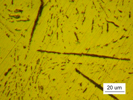
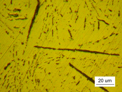
Changes in solder microstructure can influence the performance of alloys, a more uniform and fine microstructure usually means optimal solder properties. Figure 1(a)–1(f) shows the optical microstructures of as-casted SZG–xPr solders. For the SZG base alloy, the microstructure mainly consisted of β-Sn matrix and Zn-rich phases, which is the typical feature of Sn–Zn eutectic solder,Reference Chen, Hung, Lin and Su5–Reference Wei, Huang, Zhou, Zhang and Liu7 and the 0.5 wt% Ga contained in the alloy, which was hard to detect by EDS, is uniformly distributed in the matrix and grain boundaries according to previous reports.Reference Chen and Lin22–Reference Chen, Xue, Wang, Wang and Han24 When added a low content, 0.02 wt%, of Pr into the ternary alloy, it seems that the microstructure was almost the same as SZG base alloy [Fig. 1(a)]. With the increase of Pr content from 0.02 to 0.08 wt% Pr, it was found that the solder microstructures showed significant changes. The initial coarse Zn-rich phases tended to be refined as their size and volume fraction gradually decreased, as seen in Fig. 1(a)–1(c). When the Pr content reached at 0.08 wt%, the Zn-rich phases became the most homogenize and fine; a refined and uniform solder microstructure was optimized as compared to other Pr-contents solders and Sn–Zn eutectic solder (Fig. 2).
Microstructures of as-casted Sn–9Zn–0.5Ga–xPr solders: (a) SZG–0.02Pr, (b) SZG–0.04 Pr, (c) SZG–0.08Pr, (d) SZG–0.12Pr, (e) SZG–0.25Pr, (f) SZG–0.7 Pr.

Microstructure of as-casted Sn–9Zn solder.
This optimized effect can be attributed to the unique properties of RE elements. As active elements, REs tend to adsorb at the surfaces of crystal planes and grain boundaries during solidification process. According to the theory of “adsorption effect of RE” by Wu,Reference Wu and Wong30, Reference Wu, Yu, Law and Wang31 the surface free energy of the whole crystal is:
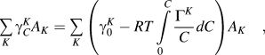
where  is the surface tension of plane K after adsorption of active materials,
 is the surface tension of plane K before adsorption,
 is the area of plane K,
 is the amount of surface-active material adsorbed at plane K, C is the concentration of surface-active material, R is the universal gas constant, and T is the absolute temperature. In order to minimize the surface free energy,
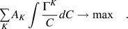
The above relationship indicates that the adsorption at crystals planes ( ) considerably affect the surface free energy of crystals. The more surface-active materials are absorbed at the interfaces, the lower surface free energy can be obtained. As a surface-active element, RE Pr prefers to accumulate at the grain boundaries and interfaces when add it to the SZG alloys. This high amount of adsorption can effectively decrease the free energy of the entire interfaces and the energy differences among crystal planes, which can prevent crystals from further growth and result in uniform and refined microstructures.Reference Wu, Yu, Law and Wang31 This is the reason why the sizes of Zn-rich phases and β-Sn grains were much finer and the whole microstructure was more homogenous in the RE-contained SZG–0.08Pr solder than that in the base alloy. The optimized microstructure then can enhance the mechanical properties according to the Hall–Petch Relationship.
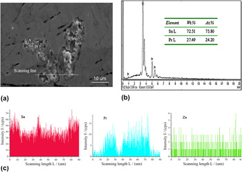
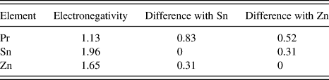
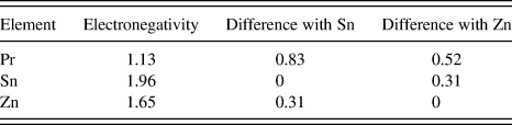
When the content of Pr was over 0.12 wt%, new dark phases formed in the Sn matrix compared, the quantity of these new phases increased with the increasing Pr content, as seen in Fig. 1(d)–1(f). Figure 3(a) shows high magnification SEM morphology of the new phase. The EDS elemental analysis implemented by point scanning [Fig. 3(b)] and line scanning [Fig. 3(c)] revealed that these phases are composed of Sn and Pr and the atomic ratio between them is approximately 3:1. Pr is not soluble in β-Sn and Zn-rich phases according to the Pr–Sn and Pr–Zn phase diagramsReference Baker and Okamoto41 and tends to accumulate at the interfaces because of its active characteristics. From the phase diagrams, Pr can react with both Sn and Zn to form IMCs, but the reaction temperature for Pr–Sn (PrSn3 IMC) is about 235 °C, which is much lower than that for Pr–Zn (above 700 °C for PrZn11), so Pr is more likely to react with Sn than Zn. In addition, the compound forming ability between two elements can be explained by the difference in their electronegativities; the greater the difference, the higher the binding force between the two elements. As shown in Table II, which lists the electronegativities of Sn, Zn, and Pr and their differences, the electronegativity difference between Sn and Pr is the greatest. This means that the formation of Pr–Sn IMCs required the lowest driving force for the solidification process; therefore, RE Pr tends to react more readily with Sn to form Sn–Pr IMCs compared to Zn. Based on above analysis and discussion, it can be confirmed that the newly formed RE-rich phases are PrSn3 IMCs. It is known that IMCs are hard brittle phases in metals and alloys, which are harmful for mechanical properties. Therefore, the content of Pr in SZG solders should be controlled to be trace amount. Otherwise, quantities of Pr–Sn IMCs would form in the microstructure, which can cause the degradation of solder properties.
Morphology of RE-rich phase in SZG–0.7Pr solder and related EDS analysis: (a) SEM image, (b) EDS analysis with point scanning, (c) EDS analysis with line scanning.

Electronegativity values of Sn, Zn, Pr, and their differences.
B. Sn whisker growth on the surface of Pr–Sn IMCs
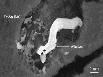
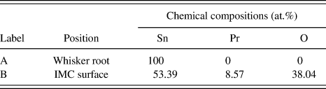
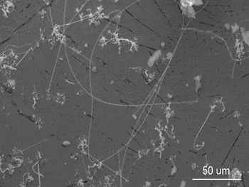
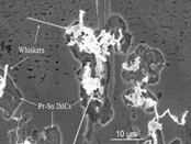
It has been documented that the application of Pb-free solder would result in the risk of Sn whisker growth on Sn-based plating finishes due to the absence of Pb in these alloys.Reference Zeng and Tu9, Reference Fukuda, Osterman and Pecht11 The present study found that the addition of RE Pr can cause a spontaneous and rapid growth of Sn whiskers in the bulk solders. As seen in Fig. 4,Reference Ye, Xue, Zhang, Xiao, Hu, Lai and Zhu42 which shows the SEM image of as-casted SZG–0.7Pr solder after exposure to ambient conditions for only half a day, it was found that a needle-like whisker appeared on the IMC surface in the solder, and related elemental analysis revealed that it was Sn whisker (Table III). Figure 5 shows the morphology of whisker growth in the solder after exposure for 30 days, numbers of varied lengths of Sn whiskers exclusively developed on the IMC surfaces. Traditionally, the observations of Sn whisker growth have been reported mainly on Sn-based thin films.Reference Shibutani, Wu, Yu and Pecht10–Reference Xian and Liu13 Some researches further concluded that the thin-film structure is a contributing factor for whisker formation, and that Sn whisker cannot be initiated on bulk lead-free solders.Reference Nychka, Li, Yangand and Chen43, Reference Tu and Li44 However, in the work described here, varying-length Sn whiskers extruded directly from the bulk solder surfaces.
Whisker growth from Pr–Sn IMC in as-casted SZG–0.7Pr solder after exposure for 12 h.Reference Ye, Xue, Zhang, Xiao, Hu, Lai and Zhu42

Whisker growth in as-casted SZG–0.7Pr solder after exposure for 30 days.

Chemical compositions at different positions of Pr–Sn IMC showed in Fig. 4 (via EDS point-scanning analysis).
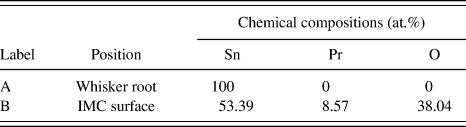
From the figures, it is worth noting that Sn whiskers only originated from the regions of Pr–Sn IMCs rather than from the entire matrix. This fact indicates that whisker growth is related to the existence of Pr–Sn compounds in the solders. Figure 3(b) and Table III show the chemical compositions of Pr–Sn IMCs before [Fig. 3(b)] and after (Table III) growing whiskers. The dramatic increase of the concentration of O implied that the Pr–Sn IMCs experienced an oxidation process during the whisker growth. As noted previously, RE Pr is an active element, thus the RE-rich PrSn3 IMCs are prone to oxide even under ambient conditions. For the possible oxide products, the Gibbs free energy of formation of Pr2O3 phase is about −1000 kJ/mol, which is much lower than that of SnO (−251.9 kJ/mol) and SnO2 (−515.8 kJ/mol) phases.Reference Speight45 Therefore, it can be stated that Pr contained in the PrSn3 phases is thermodynamically reactive and easy to react with O2 compared to Sn atoms. The oxidation reaction may take place as:

This reaction could result in a volumetric increase within Pr–Sn IMC due to the diffusion of O atoms. Since the IMCs are surrounded by Sn matrix, which constrains the IMCs from expansion, a state of local compression could result in the oxidized region. Meanwhile, according to reaction Eq. (3), fresh tin atoms would be released during the oxidation. These newly released tin atoms have a high chemical potential and can rapidly move and diffuse at room temperature.Reference Xian and Liu13, Reference Ye, Xue, Zhang, Xiao, Hu, Lai and Zhu42 It is widely accepted that the compressive stress is a necessary factor for whisker growth. Compressive stress can be induced by mechanical, thermal, and/or chemical effects.Reference Shibutani, Wu, Yu and Pecht10, Reference Dudek and Chawla39 Here, it is believed that the compressive stress generated by IMC oxidation, combined with the high chemical potential of Sn served as a driving force to squeeze tin atoms out of the oxide surface of PrSn3 phases, thus forming the tin whiskers in the solders. A deep study will be conducted on the details of driving force generation in our future study.
C. Effect of cooling rate on solder microstructures and whisker growth
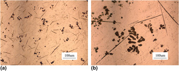
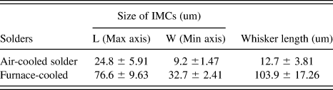
It is well known that solder microstructures are greatly affected by cooling rate.Reference Wu and Wong30, Reference Wu, Yu, Law and Wang31 The microstructures of SZG–0.7Pr solder at different cooling rates are shown in Fig. 6. In the case of fast cooling, the solder exhibited a fine and uniform microstructure with small need-like Zn-rich phases in the Sn matrix. There were also many finely dispersed small Pr–Sn IMC particles, as shown in Fig. 6(a). In contrast, the microstructural morphology showed noticeable changes in the slow-cooled solder [Fig. 6(b)]. Many coarse Zn-rich needles with over 200 microns in length appeared randomly in the matrix. The distribution of Pr–Sn IMCs was quite nonuniform and the sizes of these IMC particles were much larger compared to that in the fast-cooled solder. The distribution differences are demonstrated by the quantitative measurements shown in Table IV, which concluded the particle sizes of Pr–Sn IMCs and whisker length in SZG–0.7Pr solders under different cooling conditions. It was found that the lengths and widths of the IMCs in the slow-cooled solder were much longer and the total IMC size is approximately 11 times larger than that in the air-cooled solder.
Microstructures of SZG–0.7Pr solders at different cooling rates: (a) fast-cooled solder; (b) slow-cooled solder.

IMC and whisker distributions in SZG–0.7 Pr solders under different cooling rates (via Image J).
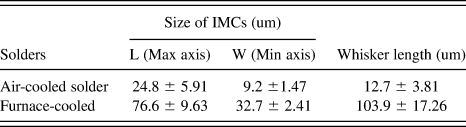
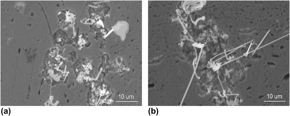
Figure 7 shows the SEM morphologies of Sn whisker growth from the Pr–Sn IMCs in SZG–0.7Pr solders under different cooling conditions after exposure to ambient conditions for 30 days. It was found that there were some noticeable features for Sn whiskers grew in these two kinds of solders. A dramatic amount of long whiskers appeared on the surfaces of large IMC particles in slow-cooled solders. In contrast to only some short whiskers formed in the fast-cooled solders, where the IMC size was correspondingly smaller than that in the slow-cooled solders. In addition, the whisker growth behaviors were also varied even in the same solder due to the nonuniform distribution of Pr–Sn IMCs. As seen in Fig. 7(b), though both large and small Pr–Sn phases coexisted in the slow-cooled solders, long and coarse whiskers appeared mainly on the surfaces of large IMCs, while it is apparently that less and shorter whiskers formed on the small IMCs. These observations reveal that there is a positive correlation between whisker growth and the size of RE-rich IMCs formed in the solder. We previously showed that whisker growth is attributed to the oxidation of Pr–Sn IMCs. The size and distribution of RE-rich IMCs is a considerable factor for the oxidation process because the IMC size can directly determine the exposed and oxidation areas.Reference Dudek and Chawla38, Reference Dudek and Chawla46 A larger IMC size means a larger exposed area and more oxidation of Pr–Sn particles, which would result in more tin atoms being released and higher compressive stress accumulated within the Pr–Sn IMCs, based on reaction Eq. (3). From Figs. 6 and 7 and the related quantitative image analysis (Table IV), it is evident that Pr–Sn phases contained in the slow-cooled solder were much larger and more closely distributed than in the fast-cooled solder. The larger IMC particles provided larger driving force and more Sn sources for whisker growth in the slow-cooled solder during exposure because of the more oxidation. As a result, whiskers grew in slow-cooled solder were much longer and more prolific than that in fast-cooled solder, where there were less Sn atoms and smaller driving force to feed whisker growth due to the smaller volume expansion during oxidation.
SEM image showing IMC distribution and Sn whisker growth in SZG-0.7Pr solders at different cooling rates: (a) small IMCs with short whiskers in fast-cooled solder; (b) large IMCs with long whiskers in slow-cooled solder.
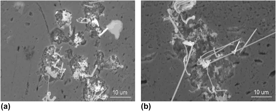
With the increasing of exposure time, Sn whiskers kept forming and developing on the solder surface. Figure 8 shows the morphology of whisker growth in slow-cooled solder after exposure for 2 mo. A significant amount of long whiskers was observed covering the entire surface. Based on above discussion, as long as oxidation continued, the compressive stress and Sn sources would be continuously provided. Thus, whiskers can form and grow until the driving force or Sn atoms are exhausted. As seen in Fig. 8, some long whiskers grew to a length of over 200 μm after 2 months exposure. It is known that the typical growth rate for Sn whisker on Sn-plating finish is 0.01–0.1 Å/s.Reference Dudek and Chawla46, Reference Ellis, Gibbons, Treuting, Doremus, Roberts and Turnbull47 This abnormal whisker growth would lead to a serious reliability concern on solder alloys.
Sn whisker growth in SZG–0.7Pr solder after exposure to ambient conditions for 2 mo.

IV. CONCLUSIONS
The effects of RE Pr on the microstructure of Sn–Zn–Ga Pb-free solder were analyzed. It was found that trace amount of RE addition can effectively refine the solder microstructure. However, the addition of RE also caused the spontaneous growth of Sn whiskers in the solder. The relationships between solder microstructure, Pr–Sn IMC, cooling rate, and whisker growth were investigated. Following conclusions were drawn from the results:
(i) The microstructure of Sn–Zn–Ga solder can be improved by adding an appropriate amount of RE Pr. However, an excessive content of Pr can lead to the formation of new RE-rich PrSn3 IMCs in the solder and thus worsen the microstructure.
(ii) Abnormal growth of Sn whiskers spontaneously takes place on the surface of PrSn3 IMCs in high Pr-content SZG–0.7Pr solder under ambient conditions. The whiskers can grow to a length of over 200 μm after 2-mo exposure. It is believed that this abnormal whisker growth is related to the oxidation of PrSn3 IMCs, which provides driving force and Sn sources to feed the whisker growth.
(iii) Cooling rate affects the solder microstructure and IMC distribution significantly as well as Sn whisker growth. The microstructure of fast-cooled solder is more uniform and finer than that of slow-cooled solder, in which the distribution of Pr–Sn IMCs is nonuniform and their size is large. Correspondingly, whisker growth in slow-cooled solder is much longer and more prolific than that in fast-cooled solder. The difference in whisker growth is attributed to the size effect of RE-rich IMCs, which affects the oxidation behaviors of IMC in different cooled solders, resulting in varied compressive stress generation and whisker growth.
(iv) Though the addition of RE Pr can greatly improve the solder microstructures, the comprehensive effects of Pr on Pb-free solders should be carefully reevaluated in case of the risk of whisker growth.
ACKNOWLEDGMENTS
This work was supported by Funding for Outstanding Doctoral Dissertation in NUAA (Project No. BCXJ11-08), and Funding of Jiangsu Innovation Program for Graduate Education (Project No. 8CXZZ11-0208). The first author also thanks the China Scholarship Council for financial support and Arvind Sai Sarathi Vasan for language help.