I. INTRODUCTION
Gallium oxide (Ga2O3) is a promising widegap semiconductor for applications including phosphors,Reference Minami1 transparent electronic devices,Reference Ueda, Hosono, Waseda and Kawazoe2–Reference Matsuzaki, Yanagi, Kamiya, Hiramatsu, Nomura, Hirano and Hosono5 deep ultraviolet photodetectors,Reference Oshima, Okuno and Fujita6, Reference Kokubun, Miura, Endo and Nakagomi7 gas sensors,Reference Ogita, Higo, Nakanishi and Hatanaka8 and spintronics devices.Reference Hayashi, Huang, Ikeno, Oba, Yoshioka, Tanaka and Sonoda9 Five polymorphs of Ga2O3, α, β, γ, δ, and ε phases, are known thus far.Reference Roy, Hill and Osborn10 Among them, the β phase with a monoclinic structure is commonly observed in Ga2O3 after firing at elevated temperatures. Although thin films of Ga2O3 typically exhibit the β phase, there are a few reports on the formation of other phases.Reference Matsuzaki, Yanagi, Kamiya, Hiramatsu, Nomura, Hirano and Hosono5, Reference Hayashi, Huang, Ikeno, Oba, Yoshioka, Tanaka and Sonoda9, Reference Shinohara and Fujita11 α-Ga2O3 with a corundum structure has been deposited on sapphire substrates by mist chemical vapor deposition.Reference Shinohara and Fujita11 Sn-doped Ga2O3 thin films on sapphire substrates fabricated by pulsed laser deposition (PLD) have been characterized as ε phase with an orthorhombic structure.Reference Matsuzaki, Yanagi, Kamiya, Hiramatsu, Nomura, Hirano and Hosono5 A recent first-principles study on the energetics of the Ga2O3 polymorphs suggested that the differences in free energy between α, β, and ε phases are small and, therefore, the polymorph of Ga2O3 is sensitively selected depending upon the preparation conditions.Reference Yoshioka, Hayashi, Kuwabara, Oba, Matsunaga and Tanaka12 In addition, doping may stabilize phases other than β.
Recently, we have demonstrated the fabrication of Mn-doped γ-Ga2O3 thin films with a defective spinel structure.Reference Hayashi, Huang, Ikeno, Oba, Yoshioka, Tanaka and Sonoda9, Reference Huang, Hayashi, Oba and Tanaka13 The films show ferromagnetism at room temperature.Reference Hayashi, Huang, Ikeno, Oba, Yoshioka, Tanaka and Sonoda9 They were grown on sapphire (0001) substrates, and two types of domain are present, each of which has an orientation relationship of γ-Ga2O3 (111) ‖ Al2O3 (0001) and either  or
 . For further understanding of the physical properties of Mn-doped γ-Ga2O3, it is important to reduce the domain boundaries and improve the crystal quality. In this paper, we report the epitaxial growth of γ-Ga2O3 thin films with a single domain on spinel (100) substrates by PLD. High crystal quality is attained by carefully optimizing the growth conditions, in particular the laser energy density. As shown in Section III-A, the films deposited under the optimized conditions show rocking curves of x-ray diffraction (XRD) peaks as narrow as those of the substrate.
II. EXPERIMENTAL PROCEDURES
The thin films were prepared by PLD using a KrF* excimer laser source (λ = 248 nm, τ = 25 ns, Lambda Physik COMPex205, Santa Clara, CA). The laser energy at the target surface was carefully controlled to be a value between 110 and 200 mJ with a standard deviation of less than 4 mJ. The laser spot size was fixed at 6.0 mm2. MgAl2O4 (100) single crystals (Shinkosha Co., Ltd., Kanagawa, Japan) were used for the substrates, which were kept at a temperature ranging from 473 to 773 K with 100 K increments. The oxygen partial pressure was set at 0.05 Pa. After the deposition, it was increased to 130 Pa and maintained at this value during cooling to room temperature. The pulsed laser with a frequency of 1 Hz was irradiated with a target-substrate distance of 65 mm. PLD targets for undoped and Mn-doped Ga2O3 with Mn concentrations of 0, 1, 2.5, 5, 7.5, 10, and 20 cation% were fabricated by mixing commercially available high-purity powders of Ga2O3 and MnO2, followed by sintering in air at 1623 K for 24 h. Powder XRD analyses found that undoped and Mn-doped targets with Mn concentrations of less than 2.5 cation% are composed of β-Ga2O3 and that Mn-doped targets with higher than 5 cation% are β-Ga2O3 and MnGa2O4. The crystal structure, crystallinity, and microstructure of the films were investigated by means of high-resolution five-axes XRD on a Rigaku SmartLab (Tokyo, Japan) (Cu-Kα, 40 kV, 30 mA), and transmission electron microscopy (TEM) and electron diffraction on a JEOL JEM3000F (Tokyo, Japan) (300 kV). The concentration of Mn in the doped films was measured by x-ray energy-dispersive spectroscopy (EDS) on the transmission electron microscope and a scanning electron microscope, JEOL JSM-6060V. To investigate the surface roughness of the films, atomic force microscopy (AFM) using a Shimadzu SPM-9500 (Kyoto, Japan) and x-ray reflectivity analysis were used.
III. RESULTS AND DISCUSSION
A. Crystal structure and crystallinity
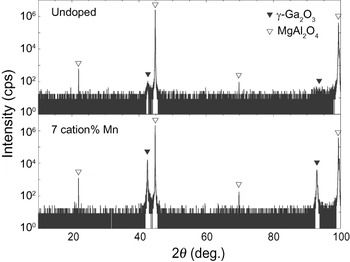
The crystal structure and crystallinity of the films were found to be sensitive to growth conditions, particularly the substrate temperature and laser energy, as well as Mn concentration. The γ-Ga2O3 films of best quality were obtained with a substrate temperature of 773 K, a laser energy of 180 mJ with a 6.0 mm2 spot size (3.0 J/cm2), and a Mn concentration of 7 cation%. Note that we were also able to obtain undoped γ-Ga2O3 films on spinel substrates under these growth conditions. The 2θ-θ XRD profiles of undoped and Mn-doped films deposited with 2000 laser pulses are shown in Fig. 1. The film thicknesses were estimated to be 65 and 70 nm through x-ray reflectivity analyses, respectively. Both 2θ-θ XRD profiles exclusively exhibit the peaks of γ-Ga2O3 and the spinel substrate. However, the crystallinity of the undoped γ-Ga2O3 film is much worse, implying that the Mn doping contributes to improving the crystal quality. Systematic XRD and TEM analyses consistently indicated that the Mn-doped films form in γ single phase and have a cube-on-cube orientation relationship with spinel substrates. As an example, the results of detailed XRD scans for the 70-nm-thick Mn-doped film deposited under the optimized conditions with 2000 laser pulses are shown in Figs. 2 and 3.
2θ-θ XRD profiles obtained using Cu-Kα1 radiation for undoped and Mn-doped films grown on spinel (100) substrates under the optimized conditions.

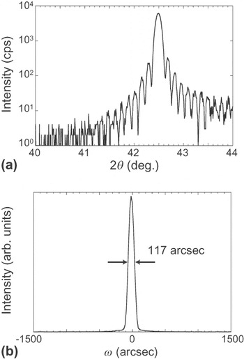
(a) 2θ-θ XRD profile around the (400) diffraction peak of the 70-nm-thick Mn-doped film. (b) Rocking curve for the (400) diffraction.

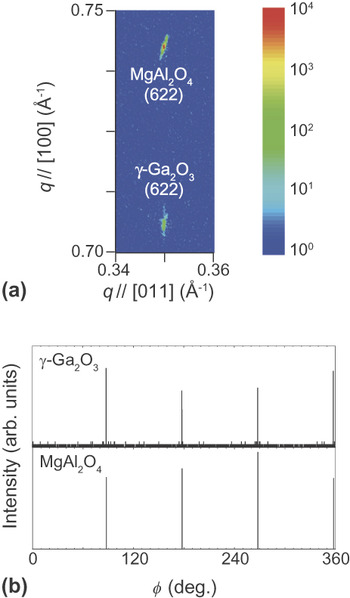
(a) Reciprocal space map around the (622) diffraction spots of the 70-nm-thick Mn-doped film and substrate. (b) φ scans of the film (upper) and substrate (lower).

A fine 2θ-θ scan around the γ-Ga2O3 (400) peak located at 42.5° is given in Fig. 2(a). It exhibits a narrow single peak accompanied by a fringe structure, which demonstrates high crystal quality of the film and uniform thickness. The film thickness estimated from the oscillation cycle of the fringe is 67 nm. The rocking curve for the (400) diffraction of the film is presented in Fig. 2(b). The full width at half maximum (FWHM) of the rocking curve is only 117 arcsec, which is close to that of the substrate (44 arcsec). Figure 3(a) shows a reciprocal space map around the (622) diffraction spots of this film and substrate. The finding that the in-plane reciprocal coordinates of the film and substrate are nearly the same indicates similarity in their in-plane lattice constants. The estimated value of the in-plane lattice constant of the film of 0.809 nm is indeed close to that of the spinel of 0.808 nm. The in-plane lattice constant is smaller than that for the out-of-plane lattice constant of 0.850 nm, corresponding to a tetragonality of 1.05. The narrow diffraction spot in the in-plane direction demonstrates that the crystal is constrained by the substrate in this direction throughout the film. As shown in Fig. 3(b), four peaks of  are placed on those of
 in the XRD φ scan, indicating the single-domain structure of the film and the cube-on-cube orientation relationship with the spinel substrate. The film and substrate show narrow peaks in the φ scan with FWHMs of 230 and 65 arcsec, respectively. We note that such high crystal quality was obtained only when the Mn concentration was varied within a range of 5 to 9 cation%. The FWHM of the rocking curves for the film decreased with increasing substrate temperature up to 773 K. Additional peaks, some of which were assigned to those from β-Ga2O3, appeared in the 2θ-θ XRD profiles of the films deposited above 873 K.
B. Microstructure
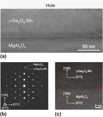
A typical cross-sectional TEM bright-field image taken from the Mn-doped film is shown in Fig. 4(a). The viewing direction is along the  zone axis for both the film and the substrate. The image contrast of the film is rather uniform and no domain boundary is observed. In addition, the film surface is flat. The film thickness estimated from the TEM image is approximately 70 nm, which agrees with the XRD result. A selected-area electron diffraction pattern obtained from an interfacial region along the
 zone axis for both the film and the substrate is shown in Fig. 4(b). The cube-on-cube orientation relationship is identified. The electron diffraction spots of the γ-Ga2O3 film along the [100] direction are clearly separated from that of the MgAl2O4 spinel substrate along the same direction, in contrast to the overlap of the two sets of diffraction spots along the [011] direction. This indicates that the Mn-doped γ-Ga2O3 film is tetragonally distorted. The diffraction patterns for regions away from the interface were found almost the same as those close to the interface, which confirms a uniform tetragonal distortion throughout the film suggested from the XRD results. A high-resolution TEM image of the interface shown in Fig. 4(c) reveals that the γ-Ga2O3 and MgAl2O4 crystals are in direct contact with each other without any interfacial layers or precipitates. To measure the concentration and distribution of Mn in the Mn-doped film, EDS analyses were performed on the TEM with a probe size of 1 nm. The results indicated a uniform distribution of Mn in the film with a concentration of 7.0 ± 0.5 cation%. The systematic TEM investigations thus confirm that the Mn-doped film is composed of the tetragonally-distorted single domain of γ-Ga2O3 without any precipitates.
(a) Cross-sectional TEM bright-field image of a region near the interface between the 70-nm-thick Mn-doped film and substrate. (b) Selected-area electron-diffraction pattern from a region containing both film and substrate. (c) High-resolution TEM image. The zone axis is  for both film and substrate. The interface is indicated by arrows.

C. Surface morphology
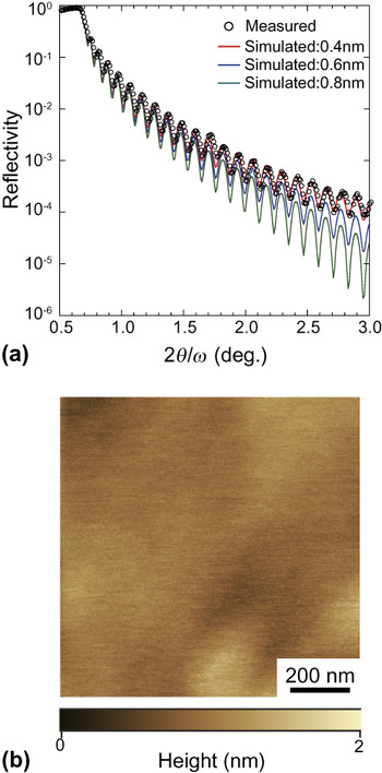
Figure 5(a) shows an x-ray reflectivity profile of the Mn-doped film, compared with simulated profiles using Parratt’s equation.Reference Parratt14 A film thickness of 70 nm, film density of 6.02 g/cm3, substrate surface root-mean-square (RMS) roughness of 0.6 nm, and film surface RMS roughness of 0.4, 0.6, or 0.8 nm are taken for the simulation. The film thickness of 70 nm was found to yield the best fit to the oscillation of the x-ray reflectivity. This value is almost the same as the thickness estimated from the fringe of the 2θ-θ XRD profile and the TEM bright-field image. Comparison with the experimental profile indicates that the RMS roughness of this film surface is approximately 0.4 nm, which is comparable to that of the spinel substrate. The flatness of the film surface was confirmed using AFM. A typical image is shown in Fig. 5(b). The RMS roughness of the film surface estimated using the AFM is approximately 0.8 nm. Thus, the film surface is rather flat.
(a) Experimental and simulated x-ray reflectivity profiles of the 70-nm-thick Mn-doped film. (b) AFM image of the film surface.

D. Preparation conditions
For the growth of high-quality γ-Ga2O3 films, we examined the effects of several parameters for PLD on the crystal structure and crystallinity. It was found that the oxygen partial pressure during deposition and pulse frequency do not affect the crystal structure and crystallinity significantly when they are varied within the ranges of 6.7 × 10⁻⁵ to 2.7 × 10⁻² Pa and 1 to 20 Hz, respectively. On the other hand, laser energy density appears to be a determinantal parameter, as well as deposition temperature and Mn concentration. The importance of the laser energy density in the PLD growth of SrTiO3 films has been recently reported by Ohnishi et al., who ascribed its effect to the change in the composition of the films.Reference Ohnishi, Koinuma and Lippmaa15, Reference Ohnishi, Lippmaa, Yamamoto, Meguro and Koinuma16 In addition, Hong et al. found that the laser energy density significantly affects the texture of ZnO films grown on Si, Kapton, and glass substrates.Reference Hong, Bae, Wang and Snyder17 These reports suggest that the laser energy density is related to both chemical and physical factors behind the crystal growth in the PLD.
In Fig. 6(a), the 2θ-θ XRD profiles for the (400) diffraction of the films deposited with three kinds of laser energy, that is, 110, 180, and 200 mJ, are compared. The number of pulses was fixed to be 2000, which yielded almost the same film thicknesses of 70 nm. The FWHMs of the rocking curves of the films deposited with laser energies of 110 and 200 mJ are 187 and 140 arcsec, respectively. These values are larger than that for the case of 180 mJ, 117 arcsec. In addition, the films deposited with laser energies of 110 and 200 mJ do not exhibit sharp fringe structures in their 2θ-θ XRD profiles, in contrast to the case of 180 mJ. The compositions of these films were found to be almost the same by the EDS analysis on the scanning electron microscope, unlike the results on SrTiO3 films reported by Ohnishi et al.Reference Ohnishi, Koinuma and Lippmaa15, Reference Ohnishi, Lippmaa, Yamamoto, Meguro and Koinuma16 We note that high crystal quality was obtained for Mn-doped γ-Ga2O3 films only when the laser energy was varied within a narrow range between 160 and 180 mJ.
(a) 2θ-θ XRD profiles obtained using Cu-Kα1 radiation for Mn-doped films grown with laser energies of 110, 180, and 200 mJ, and 2000 pulses. These films have almost the same thicknesses of 70 nm. (b) Profiles for films obtained with 180 and 200 mJ, and 10,000 pulses. The film thicknesses are 350 and 480 nm, respectively.

The 2θ-θ XRD profile of the film deposited with a laser energy of 180 mJ and 10,000 pulses is shown in Fig. 6(b). The thickness was estimated to be 350 nm by the stylus method. It exhibits a single-narrow (400) peak at 2θ = 42.53° with a FWHM of 184 arcsec, which is only approximately twice the value for the substrate, 91 arcsec. The corresponding out-of-plane lattice constant for Mn-doped γ-Ga2O3 is 0.850 nm. The narrowness of the peak indicates a small variation of the lattice constant throughout the film. For this film, the FWHM of the rocking curves is 85 arcsec. Thus, a high-quality film with a thickness of 350 nm has been grown, as well as the case of the 70 nm thickness. In contrast, when the film was deposited with a laser energy of 200 mJ and 10,000 pulses, two broad, overlapped peaks are observed in the 2θ-θ XRD profile, as shown in Fig. 6(b). The FWHMs of the rocking curves for these 2θ peaks are 440 and 1,540 arcsec, respectively. The position of the lower angle peak at 42.8° is close to that of the single peak for 180 mJ, and also to those for the 2000-pulse, 70-nm-thick films shown in Fig. 6(a). This peak is likely to originate from the region near the interface, in which the γ-Ga2O3 crystal is expected to be strongly constricted by the substrate. On the other hand, the higher angle peak can be attributed to a well-relaxed region near the film surface. For this region, the in-plane and out-of-plane lattice constants are estimated to be 0.820 and 0.826 nm, respectively, corresponding to a smaller tetragonality of 1.01. The thickness of the film deposited with 200 mJ was measured to be 480 nm by the stylus method, which is much larger than the value of 180 mJ (350 nm). This result implies that the growth rate is related to the crystallinity of the films. Our previous studies using x-ray absorption and electron energy-loss spectroscopy have suggested that most of the Mn ions are divalent and located at the tetrahedral site in γ-Ga2O3 with a defective spinel structure.Reference Hayashi, Huang, Ikeno, Oba, Yoshioka, Tanaka and Sonoda9, Reference Huang, Hayashi, Oba and Tanaka13 Its lattice constant can, therefore, be estimated by assuming Vegard’s Law between undoped γ-Ga2O3 (a = 0.824 nm)Reference Zinkevich, Morales, Nitsche, Ahrens, Rühle and Aldinger18 and spinel MnGa2O4 with Mn2+ ions at the tetrahedral site (a = 0.846 nm).Reference Boucher, Herpin and Oles19 When the Mn concentration is 7 cation%, a becomes 0.828 nm. This is close to the value obtained for the unconstrained region of the film. For a = 0.828 nm, the misfit with the spinel substrate is 2.5%. Regarding the film deposited with a laser energy of 180 mJ, a tetragonality of 1.05 is observed throughout the film with a thickness of 350 nm to reconcile the misfit, as mentioned above. It is known that the crystallinity of epitaxially-grown films is affected by the interfacial structures and energies as well as the lattice misfits between films and substrates.Reference Langjahr, Lange, Wagner and Rühle20–Reference Oba, Sugawara, Hasegawa, Izumi, Shiohara, Hirayama, Yamamoto and Ikuhara22 In addition, the behavior of the 350-nm-thick film may be related to its defective spinel structure containing intrinsically vacant Ga sites and to the presence of Mn dopants. Their arrangements can provide a large flexibility to tetragonal distortion and thereby stress relief.
IV. SUMMARY
We have demonstrated the fabrication of single-domain Mn-doped γ-Ga2O3 films with a defective spinel structure by PLD. Undoped γ-Ga2O3 films can also be grown on the spinel substrates, but the crystal quality is significantly improved by the doping of Mn. High crystal quality of Mn-doped films is attained by carefully optimizing the growth conditions, in particular the laser energy density. The films deposited under the optimized conditions show XRD rocking-curve peaks as narrow as those of the substrate. A uniform tetragonal distortion is found to take place throughout the film.
ACKNOWLEDGMENTS
This work was supported by a Grant-in-Aid for Scientific Research on Priority Area “Atomic Scale Modification” (No. 474) and the Global COE Program, both from MEXT of Japan, and the Asahi Glass Foundation Research Grant Program. H. H. thanks JSPS for the research fellowship program. R.H. was supported in part by the National Natural Science Foundation of China (Grant No. 50902051).