Introduction
This article focuses on some representative project areas in biointegrated materials science that we have found to be interesting and productive during the last decade. Much of it involves thinking about materials and devices that can integrate with biological systems in ways that were previously impossible, and pursuing the consequences in terms of advances in human health—achieved either through reductions in cost or improvements in outcomes. The emphasis is, by necessity, on our own work, but we acknowledge, at the outset, that many other groups are active in this area, with numerous examples of impressive progress beyond those described here.
A couple of particular platforms are summarized where new ideas in materials have worked well for us, and some applications are also highlighted where we are gaining good traction in clinical translation. Much of this work is ultimately about having a positive effect on how we think about human healthcare and about building devices that can improve the lives of patients who are suffering from various kinds of disorders. Another area that represents a frontier in this broader space is three-dimensional (3D) open-network systems that integrate with biology through volumetric spaces, rather than surfaces, to enable new levels of functionality.
We think about the key challenges in the context of reformulating or reengineering the kinds of sophisticated electronic devices that form the backbone of consumer gadgetry, into systems that can support long-term, intimate integration with soft tissues of the human body. We focus on those kinds of interfaces and capabilities, in terms of their use for human health, neuroscience research, and discovery, as tools to improve our understanding of living systems and to improve human health as well.
In terms of various organ systems as points of integration, one obvious area of opportunity is the brain—biology’s most sophisticated form of electronics. If one wants to understand how the brain operates, or if one wants to deliver engineered therapies to address brain disorders, one might want to bring to bear on that problem man’s most sophisticated form of electronics—integrated circuits that incorporate high-performance transistor and logic functionality. Standard, wafer-based platforms that form the basis of cell phones and laptop computers do not work well in this context. New materials strategies and new device designs are required to render that type of functionality into biocompatible forms; for example, thin, soft membranes that gently laminate onto the textured surfaces of the brain, with capabilities also for integration with the heart and the skin. As an aspirational goal, one can think about materials approaches that can support a broad set of microsystems technologies, not just electronics but optoelectronics, microfluidics, microelectromechanical systems, and others, in architectures and with design principles that allow for interfaces with biology in ways that have not been possible in the past.
To think about this goal, one needs to step back and consider key design paradigms in biology, not necessarily with the idea of replicating those features, but for abstracting the essential characteristics to allow for a merging of technology and biology in ways that could have powerful consequences. One can think about biology as hierarchical, with a broad range of length scales, reconfigurable, transient, self-healing, heterogeneously integrated with combinations of hard and soft materials together, multifunctional and with 3D network architectures. Beyond the academic question of how one might build these materials systems, what kinds of key features could be adapted from biology for technologies that can interface with living organisms over long periods with new functional possibilities?
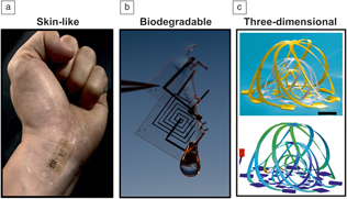
Three areas have been of interest to us in this broader context, as summarized in Figure 1. The first is in electronics that involve thin, skin-like architectures—soft membranes that reside on the surfaces of organsReference Kim, Lu, Ma, Kim, Kim, Wang, Wu, Won, Tao, Islam, Yu, Kim, Chowdhury, Ying, Xu, Li, Chung, Keum, McCormick, Liu, Zhang, Omenetto, Huang, Coleman and Rogers1–Reference Xu, Gutbrod, Bonifas, Su, Sulkin, Lu, Chung, Jang, Liu, Ying, Lu, Webb, Kim, Laughner, Cheng, Liu, Ameen, Jeong, Kim, Huang, Efimov and Rogers3 or cellular-scale filaments that penetrate into their depths.Reference Kim, McCall, Jung, Huang, Siuda, Li, Song, Song, Pao, Kim, Lu, Lee, Song, Shin, Al-Hasani, Kim, Tan, Huang, Omenetto, Rogers and Bruchas4–Reference Lu, Gutruf, Xia, Bhatti, Wang, Vazquez-Guardado, Ning, Shen, Sang, Ma, Pakeltis, Sobczak, Zhang, oh Seo, Xue, Yin, Chanda, Sheng, Bruchas and Rogers6 We and other groups have started to explore skin-like electronics not just for the skin, but for the brain and neural tissues,Reference Won, Song, Zhao, Li, Rivnay and Rogers7 the heart, the peripheral nervous system, the spinal cord, the bladder, and others. The second is a stream of work based around the idea of biodegradable or “transient” electronics—systems that operate in a time-coordinated fashion with a transient biological process such as wound healing, and then eliminate themselves through natural biological mechanisms into surrounding biofluids, thereby expelling the device load from the body in a natural way after the function is no longer needed.Reference Hwang, Tao, Kim, Cheng, Song, Rill, Brenckle, Panilaitis, Won, Kim, Song, Yu, Ameen, Li, Su, Yang, Kaplan, Zakin, Slepian, Huang, Omenetto and Rogers8–Reference Kang, Koo, Lee and Rogers12 The third area—a frontier, exploratory area—involves efforts to render electronics into controlled, deterministic 3D mesoscale frameworks that can serve as active electronic, optoelectronic scaffolds for growth of tissues and cells in fundamental studies or for interfaces to engineered organoids.Reference Xu, Yan, Jang, Huang, Fu, Kim, Wei, Flavin, McCracken, Wang, Badea, Liu, Xiao, Zhou, Lee, Chung, Cheng, Ren, Banks, Li, Paik, Nuzzo, Huang, Zhang and Rogers13–Reference Fu, Nan, Bai, Huang, Bai, Lu, Zhou, Liu, Liu, Wang, Han, Yan, Luan, Zhang, Zhang, Zhao, Cheng, Li, Lee, Liu, Fang, Li, Huang, Zhang and Rogers15
Images and illustrations of opportunities for materials in three areas of interest in biointegrated electronic/microfluidic systems. (a) Image of a “skin-like” electronic device on the wrist. (b) Biodegradable circuit partially dissolved by a drop of water. (c) Three-dimensional electronic framework. The upper image is a colorized scanning electron microscope image of a nested set of basket-shaped structures. The bottom image corresponds to computational results based on finite element modeling. Scale bar = 400 μm.

Materials approaches
In each of these three areas, the core challenges are in materials science. How do you begin to build such devices, and what kind of materials and architectures might be interesting? The first part of this question might address the semiconductor, the most daunting materials challenge in any kind of electronic or optoelectronic technology. One can consider many different classes of emergent materials—carbon nanotubes, semiconductor nanowires, graphene, two-dimensional (2D) materials, polymers, and small molecules. An alternative strategy might seek highly unconventional ways to exploit well-established materials, those that already serve as the bedrock of consumer electronic devices. Our greatest successes have followed from the latter, where, as an example, the use of monocrystalline silicon and other inorganic materials are formatted into micro-/nanostructured forms and combined with soft polymer supports and matrices in carefully engineered ways to achieve the overall shapes and mechanical properties that are necessary for chronic biointegration.
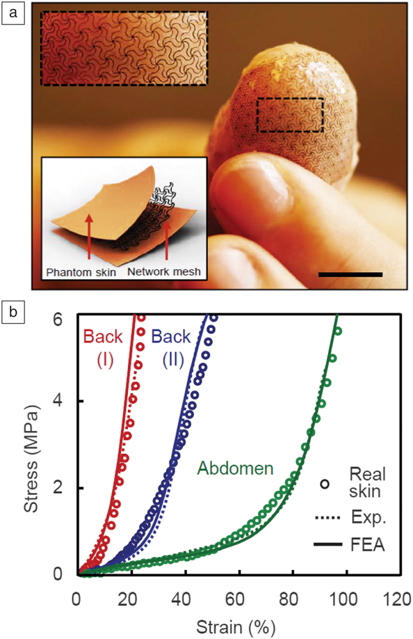
The strategies to deploy silicon, as an example, in this manner can be viewed as a form of composite engineering, in the sense of designing combinations of hard and soft materials with deterministic, optimized layouts to meet combined considerations in function, mechanics, and form.Reference Kim, Lu, Ma, Kim, Kim, Wang, Wu, Won, Tao, Islam, Yu, Kim, Chowdhury, Ying, Xu, Li, Chung, Keum, McCormick, Liu, Zhang, Omenetto, Huang, Coleman and Rogers1,Reference Rogers, Someya and Huang16–Reference Xu, Zhang, Jia, Mathewson, Jang, Kim, Fu, Huang, Chava, Wang, Bhole, Wang, Na, Guan, Flavin, Han, Huang and Rogers21 For instance, nanoscale, thin filamentary ribbons of silicon and other well-established electronic materials, configured into open, spider web networks with well-defined, optimized layouts and embedded in thin, soft silicone matrices yield systems with physical properties that can be controlled precisely. With quantitative attention to the details of the mechanics of such hard/soft constructs, these designer materials can support wide-ranging types of advanced high-performance electronic functionality with mechanical properties, as measured by equivalent stress–strain responses that quantitatively line up with those of targeted biological systems such as the skin.Reference Kim, Lu, Ma, Kim, Kim, Wang, Wu, Won, Tao, Islam, Yu, Kim, Chowdhury, Ying, Xu, Li, Chung, Keum, McCormick, Liu, Zhang, Omenetto, Huang, Coleman and Rogers1,Reference Jang, Chung, Xu, Lee, Luan, Jeong, Cheng, Kim, Han, Lee, Kim, Cho, Miao, Yang, Jung, Flavin, Liu, Kong, Yu, Rhee, Chung, Kim, Kwak, Yun, Kim, Song, Paik, Zhang, Huang and Rogers19 For instance, effective moduli of these composites can be tailored to reach 160 kPa, a value similar to that of human skin, but with silicon, a material that has a modulus of 150 GPa, as the active semiconductor. It is possible to create artificial systems that offer the kind of electronic functionality that one would want with the necessary mechanics and geometric conformality.
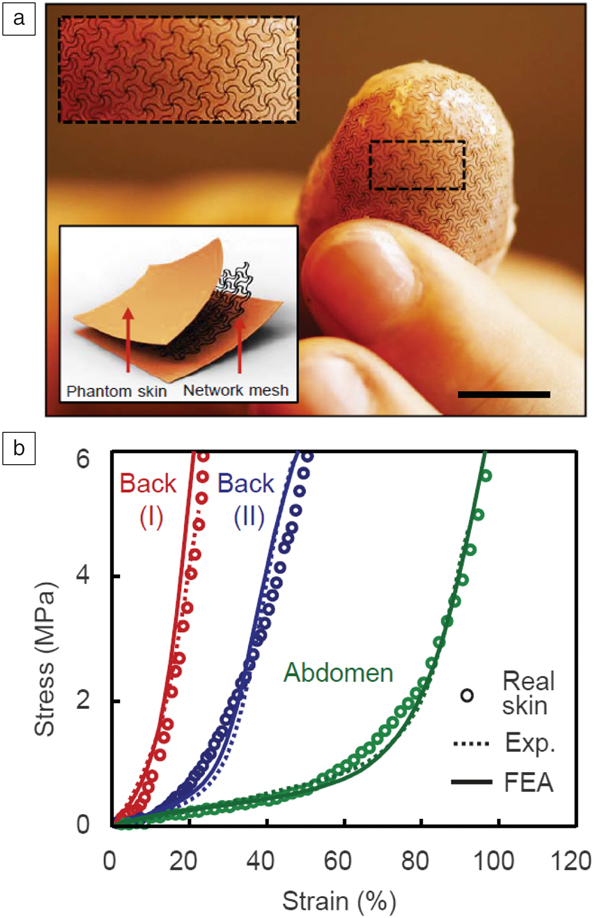
These general concepts provide frameworks for dropping in different types of materials and devices. With close attention to the finer details, guided by computational modeling, mesh-like architectures in these hard/soft composites can be designed to match not only the linear regime modulus of a soft biological tissue, but also the full J-shaped stress–strain responses.Reference Jang, Chung, Xu, Lee, Luan, Jeong, Cheng, Kim, Han, Lee, Kim, Cho, Miao, Yang, Jung, Flavin, Liu, Kong, Yu, Rhee, Chung, Kim, Kwak, Yun, Kim, Song, Paik, Zhang, Huang and Rogers19 Here, buckling mechanics and strain-limiting characteristics that flow from these kinds of open-network meshes, following from inverse design and computation, underpin the resultant effective mechanical characteristics.
As an example, we can achieve experimentally measured stress–strain responses in deterministic composites that match the full, nonlinear response of skin collected from different regions of the body—two spots on the back and one on the abdomen—quantitatively,Reference Jang, Chung, Xu, Lee, Luan, Jeong, Cheng, Kim, Han, Lee, Kim, Cho, Miao, Yang, Jung, Flavin, Liu, Kong, Yu, Rhee, Chung, Kim, Kwak, Yun, Kim, Song, Paik, Zhang, Huang and Rogers19 as shown in Figure 2. These results can be achieved even with simple geometric architectures in the mesh constructs.
(a) Images and schematic illustrations of a thin, deterministic hard/soft composite structure designed for integration with the skin. Computationally guided choices of the geometries of the mesh structures in such systems allows for quantitative matching of the effective mechanical properties of these materials to biological tissues. Scale bar = 1 cm. (Top inset) Magnified view of the dashed box. (Bottom inset) The schematic illustration shows the multilayer construction of this composite material. (b) Example of full nonlinear stress–strain responses tailored to match the properties of skin at different locations on the human body: two locations on the back and one on the abdomen. Note: Exp, experimental; FEA, finite element analysis.Reference Jang, Chung, Xu, Lee, Luan, Jeong, Cheng, Kim, Han, Lee, Kim, Cho, Miao, Yang, Jung, Flavin, Liu, Kong, Yu, Rhee, Chung, Kim, Kwak, Yun, Kim, Song, Paik, Zhang, Huang and Rogers19
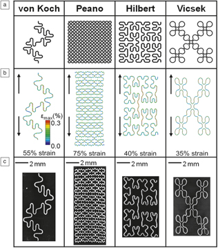
Additional sophistication in design follows from the use of fractal mathematics, where different basis sets serve for filling 2D spaces with thin filaments using systematic iterative rules. Important mechanics consequences follow from the inherent self-similarity of the fractal geometriesReference Fan, Yeo, Su, Hattori, Lee, Jung, Zhang, Liu, Cheng, Falgout, Bajema, Coleman, Gregoire, Larsen, Huang and Rogers20 (see Figure 3). Specifically, hierarchical arrays of interconnected springs associated with these layouts yield highly favorable mechanical properties. These generic, powerful schemes allow for construction of broad classes of active, electronic systems built into frameworks that act as mechanical metamaterials for purposes of biointegration, where the chemistry at the biointerface is chosen based on materials with known biocompatibility.
Fractal concepts in composite design. (a) Geometric forms where the top row identify the different fractal curves. (b) Computed mechanical responses; the arrows indicate the direction of uniaxial strain. (c) Experimental results for filamentary structures of silicon with several representative fractal layouts. The results highlight the mechanical responses of filamentary structures in various fractal curves. Note: εmax, maximum principal strain.Reference Fan, Yeo, Su, Hattori, Lee, Jung, Zhang, Liu, Cheng, Falgout, Bajema, Coleman, Gregoire, Larsen, Huang and Rogers20

Epidermal electronics
We developed systems for skin-integration initially back in 2011Reference Kim, Lu, Ma, Kim, Kim, Wang, Wu, Won, Tao, Islam, Yu, Kim, Chowdhury, Ying, Xu, Li, Chung, Keum, McCormick, Liu, Zhang, Omenetto, Huang, Coleman and Rogers1 and then improved on these in 2014,Reference Xu, Zhang, Jia, Mathewson, Jang, Kim, Fu, Huang, Chava, Wang, Bhole, Wang, Na, Guan, Flavin, Han, Huang and Rogers21 with the ability to build advanced wireless sensor devices in skin-like or tissue-like forms. Many other groups also contributed to this broader field through materials and mechanics innovations of their own.Reference Ray, Ghaffari, Bandodkar, Krishnan, Choi and Rogers22,Reference Heikenfeld, Jajack, Rogers, Gutruf, Tian, Pan, Li, Khine, Kim, Wang and Kim23 The kind of functionality one can now bring to bear on the skin, via these collective efforts of the broader community, opens up enormous possibilities in physiological monitoring and therapy. It is more than the mechanics that one is tailoring to the skin; structures that can conform to the irregular surfaces of the skin are also possible, with a collection of additional properties in thermal load, mass density, water transport, and others that support a stable biointerface.
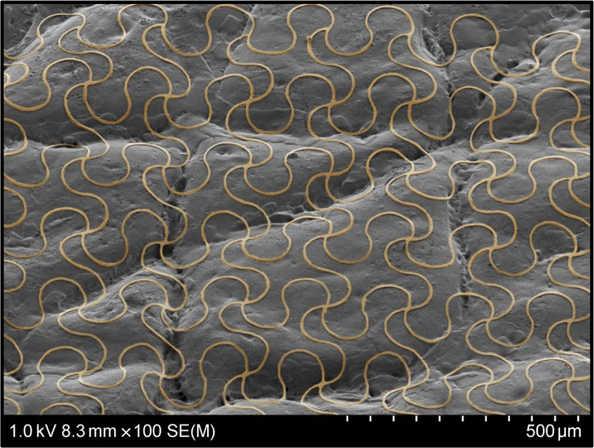
Colorized scanning electron micrographs of a representative mesh-like frameworks mounted on a polymer replica of human skin illustrate the way that this kind of filamentary serpentine structure can adapt to very complex contoured shapes (Figure 4). This feature is important not only because it facilitates adhesion to these soft, time-dynamic surfaces, but also because it minimizes thermal and electrical impedances for measurements that use the skin as a window for monitoring underlying physiological processes. These platforms are radically different from the technology approaches that support wearables currently available as consumer devices—wrist-mounted, rigid blocks of electronics loosely coupled to the body—because their form of integration allows for classes of clinical measurements that demand physical contact with the skin, but without the restrictions for use in a hospital or laboratory setting. They support, for example, continuous monitoring of electrocardiogram traces—not just heart rate but the full wave forms that cardiologists understand based on decades of experience.
Colorized scanning electron microscope image of a filamentary serpentine structure in contact with a polymer replica of human skin. The deformability of the mesh allows for intimate interfaces to the types of complex, textured surfaces often encountered in biology.

The pre-existing database and knowledge surrounding this type of measurement can support actionable recommendations based on detailed signatures. Other measurements that require physical contact with the skin are also possible in continuous modalities outside of labs and hospitals.Reference Rogers, Malliaras and Someya24 Examples include assessments of the hydration level of the skin, typically measured with a hand-held Corneometer device, and continuous pressure measurements using piezoelectric materials to capture the time dynamics of pulsatile blood flow through near-surface arteries to reproduce arterial tonometry, a clinical measurement of blood pressure in the arteries, are currently performed only in the hospital.Reference Ray, Ghaffari, Bandodkar, Krishnan, Choi and Rogers22,Reference Heikenfeld, Jajack, Rogers, Gutruf, Tian, Pan, Li, Khine, Kim, Wang and Kim23
One stream of work is to take these kinds of platforms and reproduce the sorts of measurements that are performed in the hospital. The other is to exploit them for purposes that are currently not possible (i.e., to go beyond what is done clinically). One example is the ability to perform extremely high-precision thermal measurements and thermal mapping of temperature distributions across the surfaces of the skin with milli-Kelvin precision.Reference Webb, Bonifas, Behnaz, Zhang, Yu, Cheng, Shi, Bian, Liu, Kim, Yeo, Park, Song, Li, Huang, Gorbach and Rogers25 Further engineering refinements allow for the ability to dose in very precise, tiny amounts of thermal power to allow for measurements of the time dynamics of heat flows through the skin. With such a device, configured with a central thermal actuator and a constellation of precision temperature sensors around it, positioned over a near-surface artery or vein, it is possible to quantify spatial asymmetries in temperature distributions that are suitable can, with the use of computational models, yield the determinations of the volumetric flow rates of blood through these macrovessels.Reference Webb, Ma, Krishnan, Li, Yoon, Guo, Feng, Shi, Seidel, Cho, Kurniawan, Ahad, Sheth, Kim, Taylor, Darlington, Chang, Huang, Ayers, Gruebele, Pielak, Slepian, Huang, Gorbach and Rogers26 Such flow measurements can be reproduced with a laser Doppler system, but they are not routinely performed clinically due to the cumbersome nature of the supporting hardware and the extreme sensitivity to motion artifacts. With a skin-like piece of electronics, configured with the thermal functionality outlined previously, the measurement is quite straightforward and can be performed continuously in a noninvasive way. Comparisons of laser Doppler measurements of occlusion, or blockage, and then reperfusion, or release, performed simultaneously with this kind of thermal approach using these skin-like devices, show quantitative agreement.Reference Webb, Ma, Krishnan, Li, Yoon, Guo, Feng, Shi, Seidel, Cho, Kurniawan, Ahad, Sheth, Kim, Taylor, Darlington, Chang, Huang, Ayers, Gruebele, Pielak, Slepian, Huang, Gorbach and Rogers26
These platforms can be used for various thermal and electrical, fluidic, mechanical, optical, and mechano-acoustic measurements of body processes,Reference Ray, Ghaffari, Bandodkar, Krishnan, Choi and Rogers22,Reference Heikenfeld, Jajack, Rogers, Gutruf, Tian, Pan, Li, Khine, Kim, Wang and Kim23 with many that are ready for scaled deployment.Reference Rogers, Malliaras and Someya24 There has been tremendous interest from the clinical community for devices of this type, and we are now involved in more than 20 different human clinical studies, ranging from devices that are used in the operating room for monitoring in the context of surgical interventions on the spine,Reference Liu, Tian, Raj, Cotton, Ma, Ma, McGrane, Pendharkar, Dahaleh, Olson, Luan, Block, Suleski, Zhou, Jayaraman, Koski, Aranyosi, Wright, Jayaraman, Huang, Ghaffari, Kliot and Rogers27 to those that deploy across multiple positions on patients who are suffering from Parkinson’s disease.Reference Lonini, Dai, Shawen, Simuni, Poon, Shimanovich, Daeschler, Ghaffari, Rogers and Jayaraman28 In this latter case, it is possible to pick up early signs of tremors by applying machine learning to full body kinematics captured in this way.Reference Lonini, Dai, Shawen, Simuni, Poon, Shimanovich, Daeschler, Ghaffari, Rogers and Jayaraman28 We are deployed on stroke patients as well, with collaborators at the AbilityLab in Chicago and we are especially interested in maternal, fetal, and neonatal health. (Video 1)Footnote *
Epidermal microfluidic analysis systems
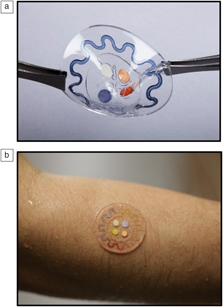
One interesting device platform is a microfluidic lab-on-a-chip technology rendered in materials such as silicones and elastomeric copolymers, that are skin-compatible: soft, conformal, and able to adhere tightly to the surface of the skin to allow for the capture of minute volumes of sweat as it emerges from the skin for biomarker detection in situ, in real time.Reference Koh, Kang, Xue, Lee, Pielak, Kim, Hwang, Min, Banks, Bastien, Manco, Wang, Ammann, Jang, Won, Han, Ghaffari, Paik, Slepian, Balooch, Huang and Rogers29 In this manner, we can expand the mode of operation of skin-interfaced devices from the biophysical into the realm of biochemical assays. These platforms are fully integrated systems, with arrays of microchannels and valving technologies, with small, self-contained reservoirs into which we load colorimetric chemical reagents that respond to a biomarker of interest through a color change. We can quantitatively capture sweat rate, sweat loss, and as well as electrolyte loss, glucose and lactate concentration, and pH. Related strategies from other groups can also provide access to these and other sorts of measurements using other schemes.Reference Choi, Ghaffari, Baker and Rogers30
Figure 5 shows an example of one of these devices, with serpentine channels that allow visualization of the filling front; the volume of sweat in the channel and the size of the inlet port through which sweat is being pumped into the system are known. As a result, we can determine the local sweat rate. The local sweat rate for an individual can be calibrated to full body sweat rate and sweat loss,Reference Choi, Ghaffari, Baker and Rogers30 which is important not only for clinical medicine but also for sports and other scenarios. The idea of using colorimetric approaches, without any electronics, allows for a cost structure that enables one-time use without the need for cleaning and sterilizing. The construction is simple—a molded piece of silicone with a biomedical adhesive on the backside along with embedded color-responsive chemistries. The example of Figure 5 has capabilities for measuring chloride, glucose, pH, and lactate levels, with additional temperature measurements via thermochromic liquid crystals.
Optical images of (a) a freestanding and (b) skin-integrated soft, microfluidic system designed for capture, storage, manipulation, and biomarker analysis of microliter volumes of sweat released from the surface of the skin.

In the context of patients who have suffered from a stroke, right-left body asymmetries appear in sweat rate because of the nature of the brain impairment. These asymmetries can serve as metrics to determine the progression of a patient through a rehabilitation routine, so that the protocols can be tailored to the individual. We have deployed these devices on approximately 50 stroke patients so far for measuring these asymmetries, not only for sweat rate but also for sweat chemistry. They can also be used for screening for cystic fibrosis, which is typically performed via measurements of electrolyte concentration in sweat with a hockey-puck-type device that is tightly strapped to the arms of infants. Our platform provides an attractive alternative. Sports and athletics are additional areas of opportunity, and these devices have been used on various professional athletes in American football and also on professional baseball players during games.
Monitoring of flow through shunts in patients with hydrocephalus
In terms of fluidics, as described previously, noninvasive quantitation of blood flow is possible using skin-interfaced thermal dilution-type approaches that rely on changes in distributions of temperature associated with flow effects. The work was originally performed in an open-ended, academic discovery mode, but later, we were alerted to the clinical utility of this type of platform. Specifically, we received inquiries from physicians about the possibility of measuring flow of cerebrospinal fluid through ventricular shunts used to treat hydrocephalus.
Approximately 1 million people in the United States suffer from hydrocephalus, a disorder that affects the ability of the body to regulate the pressure of the cerebrospinal fluid in the intracranial space. Shunts are tubes that pass from the ventricles in the brain down to a distal part of the body, sometimes the abdomen, such that flow through the shunt can relieve excessive pressures. The problem with shunts is they have a 100% failure rate—it is just a matter of time before they become clogged, kinked, or broken in a way that prevents flow and results in the potential for profound negative health consequences for the patient. Hydrocephalus can either be congenital or it can result from traumatic brain injury or other conditions. Shunts are the only solution, and the symptoms of failure are nonspecific. Due to the uncertainties, patients are typically forced to make trips to the hospital for computer tomography (CT) scans and x-rays, and sometimes surgical procedures, to determine the status of the shunt.
One of our patients is 26 years old and has already had nearly 190 surgical procedures and hundreds of CT and x-ray scans associated with malfunctioning shunts. Here, we were able to take our skin-interfaced blood flow measurement devices, adapt them, and deploy them for this particular application. We recently published a systematic study of the physics and materials science of these devices, along with a critical mass of clinical data based on their use with hydrocephalus patients.Reference Krishnan, Ray, Ayer, Ma, Gutruf, Lee, Lee, Wei, Feng, Ng, Abecassis, Murthy, Stankiewicz, Freudman, Stillman, Kim, Young, Goudeseune, Ciraldo, Tate, Huang, Potts and Rogers31 At the most basic level, the measurement signal provides a strong, unambiguous method to differentiate between flow and no flow; even this binary piece of information turns out to be extremely important. (Video 2)Footnote **
Assembly of 3D, open-mesh electronics
The devices discussed thus far take the form of thin membranes that interact with the surfaces of organ systems. In addition to skin, they can deploy onto the epicardium, the outer surface of the cardiac muscle, the surface of the brain, the bladder, or many other areas. The ability to laminate onto such surfaces and then for the devices to peel away allows for noninvasive or minimally invasive modes of operation, but ultimately, biology involves 3D architectures as a ubiquitous design paradigm; understanding biology requires more than measurements on surfaces. Open scaffolds of neural circuits, vasculature networks, and cytoskeletal meshes represent open 3D geometries of interest. For a number of years, we considered different strategies that would allow us to configure planar device technologies—electronics, optoelectronics, microfluidics—in a manner such that flipping a switch could induce a controlled transformation into a well-defined 3D network architecture with engineering precision and control. We almost concluded that such a scheme might not exist, but then we stumbled onto an approach that is both extremely effective and remarkably easy, with a set of concepts that apply naturally to the most advanced 2D microsystem technologies.Reference Xu, Yan, Jang, Huang, Fu, Kim, Wei, Flavin, McCracken, Wang, Badea, Liu, Xiao, Zhou, Lee, Chung, Cheng, Ren, Banks, Li, Paik, Nuzzo, Huang, Zhang and Rogers13–Reference Fu, Nan, Bai, Huang, Bai, Lu, Zhou, Liu, Liu, Wang, Han, Yan, Luan, Zhang, Zhang, Zhao, Cheng, Li, Lee, Liu, Fang, Li, Huang, Zhang and Rogers15 The results go well beyond anything that is possible with 3D printing, simply because it is currently not possible to print silicon transistors, for example, with nozzles or inkjets or stereolithographic setups.Reference Zhang, Zhang, Yan, Ma, Li, Huang and Rogers32
Here, wafers populated with fully integrated devices on their surfaces can be configured to allow liftoff of functional structures into thin, 2D open filamentary mesh geometries similar to those described previously for skin-integrated devices. These mesh constructs are bonded to a prestrained elastomer substrate, but only at select, lithographically defined locations, by appropriate tailoring of the surface chemistries. Relaxing the prestrain imparts in-plane stresses that induce a buckling process to geometrically transform these 2D platforms into 3D architectures in a deterministic, parallel way that provides access to a wide range of 3D geometries and length scales, from nanometers to centimeters and beyond, in nearly all classes of planar thin-film materials and device technologies.
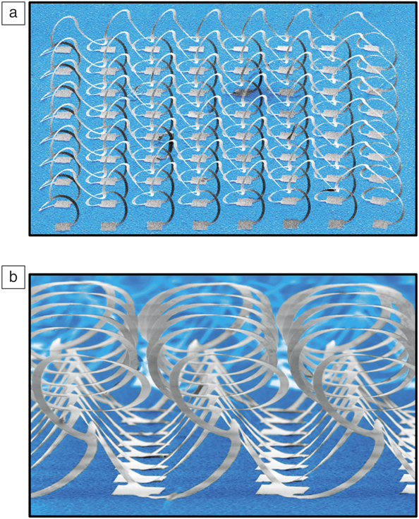
Finite element modeling captures the process quantitatively. Starting from a two-dimensional planar layout, release of strain in the substrate causes the structure to move—in parallel and across large areas in a simultaneous manner—into a 3D geometry by translating, buckling, rotating, and twisting in a coordinated manner. The 3D architecture that results has a layout that is predetermined by the 2D geometry of the precursor, the locations of the bonding sites, and the nature and magnitude of the prestrain. Although this scheme represents a powerful and simple idea, it allows access to all kinds of different geometries, in a manner that is compatible with the most advanced materials technologies. In the example shown in Figure 6, monocrystalline silicon microstructures transform into a 3D network-type design through application of this approach. This example is a thin-film, filamentary network structure; since it is silicon derived from a wafer source, it is straightforward to integrate silicon-based devices onto the surfaces to yield full 3D functional systems.
(a) Low and (b) high magnification colorized scanning electron micrographs of a representative 3D mesoscale framework of monocrystalline silicon ribbons (widths of 50 μm and thicknesses of 1.5 μm) on a silicone support. Mechanically guided assembly techniques transform planar precursors into these structures.Reference Xu, Yan, Jang, Huang, Fu, Kim, Wei, Flavin, McCracken, Wang, Badea, Liu, Xiao, Zhou, Lee, Chung, Cheng, Ren, Banks, Li, Paik, Nuzzo, Huang, Zhang and Rogers13

A natural next question is how can this be integrated with biology. One possibility is to use the structure as an open scaffold for growing tissues in and around the supporting filaments in a way that allows interaction with cells for monitoring and stimulating their proliferation, differentiation, and formation of network connections. We have explored this strategy with neurons extracted from the dorsal root ganglion, a region of the spinal cord, of rat models. Here, we are using 3D structures instrumented with electrodes for the types of multielectrode array analyses that have been completed previously in 2D, but in more naturalistic 3D geometries that accurately capture the way the cells are ultimately configured in real biological systems. We seed cells onto these types of devices and measure their activity at the individual cell level using instrumentation intrinsically embedded onto 3D basket-type structures.Reference Yan, Han, Shi, Badea, Yan, Kulkarni, Hanson, Kandel, Wen, Zhang, Luo, Lin, Zhang, Guo, Huang, Nan, Jia, Oraham, Mevis, Lim, Guo, Gao, Ryu, Yu, Nicolau, Petronico, Rubakhin, Lou, Ajayan, Thornton, Popescu, Fang, Sweedler, Braun, Zhang, Nuzzo, Huang, Zhang and Rogers14
This frontier area appears to be interesting for materials research at the intersection with medicine and biology. Modeling tools can be used for inverse design, thereby opening access to broad ranges of desired shapes and geometries matched to biological outcomes. Compatibility extends to the entire range of materials, from semiconductors and metals to dielectrics, hydrogels, silicon, 2D materials, and conducting polymers.
Conclusions
We conclude by returning to the three different areas that we feel are exciting for research in electronic materials at the interface with biology. The first is in biocompatible skins—soft laminates that can interface with the body. The second area—biodegradable electronics—was not covered extensively here, but it represents a significant, ongoing effort in our group. The third is 3D microsystems. Materials science plays a critical, foundational role in these areas, and emerging opportunities in both basic and applied research suggest a promising future for this field.
Acknowledgments
I am deeply honored and fortunate for our research to be recognized in this manner. The list of folks who have received the MRS Medal is amazing, but an award such as this is given for a body of work, not to an individual. For me, that means a very large collection of students, postdocs, and collaborators; they are the real winners here, and my name just happens to be attached to the award.

John A. Rogers is the Louis Simpson and Kimberly Querrey Professor of Materials Science and Engineering, Biomedical Engineering, and Neurological Surgery at Northwestern University, where he is also director of the Center for Bio-Integrated Electronics. He has published more than 650 papers, and his research has been recognized by many awards, including a MacArthur Fellowship, the Lemelson-MIT Prize, and the Smithsonian Award for American Ingenuity in the Physical Sciences. He is a member of the National Academy of Engineering, the National Academy of Sciences, and the American Academy of Arts & Sciences. Rogers can be contacted by email at jrogers@northwestern.edu.