I. INTRODUCTION
The next generation of wireless telecommunication and radar systems requires wideband high-power amplifiers (HPAs) to be able to handle multiple bands and operating standards. In addition, high efficiency and compact size will also be required if the HPAs are used in a mobile platform because HPAs are the most energy-consuming components in wireless telecommunication and radar transmitters. A single multi-band HPA will offer cost reduction and reduced inventory requirement.
Today, GaN devices address high power and high efficiency with wideband performances. It offers high breakdown voltage, which allows large drain voltages to be used, leading to high output impedance per watt of radio frequency (RF) power, resulting in easier matching and lower loss matching circuits compared to LDMOS technologies. United monolithic semiconductor (UMS) is a leading-edge European foundry developing GaN technologies and products since many years.
The generation of high-power, efficiency enhancement techniques and broadband amplifiers concept became an important topic over the last few years.
A common approach of efficiency enhancement is harmonic tuning [Reference Cripps1, Reference Cripps, Tasker, Clarke, Lees and Benedikt2]. However, such amplifiers are only used for narrowband applications with up to 10–20% fractional bandwidths. Moreover, for high-efficiency classes of operation, it is difficult to maintain appropriate higher harmonic loading conditions over more than one octave of bandwidth. Although the range can be somewhat extended by a balanced design, inevitably the highest fundamental frequencies will overlap the lowest second harmonic frequencies.
For the design of wideband amplifiers, one of the most popular techniques is the distributed [Reference Campovecchio, Obregon, Lajugie and Le Bras3] approach.
Analytic calculations we have performed show that, for maximum power added efficiency (PAE), the bandwidth of distributed amplifiers (without dummy load in the drain transmission line) is slightly wider than the one obtained in a reactive matched parallel configuration. Nevertheless, the out of band stability remains a problematic issue often leading to a limitation of the overall efficiency.
In this paper, the design, advanced realization, and characterization of highly efficient HPAs with more than one octave bandwidth are presented. On the other hand, time-domain measurements have been performed at very high sampling frequencies (80 GS/s) to show the experimental performances of the HPAs before and after application of simple linearization technique.
A design procedure is proposed in Section II. It is based on source-pull/load-pull simulation approaches. A theoretical study of the limitations in terms of trade-off between bandwidth and efficiency is applied to the 0.5 µm GaN GH50 technology from UMS foundry. A single-ended MIC externally matched, a single-ended and a balanced Quasi-MMIC internally matched amplifiers have been designed with this method. Experimental results in terms of bandwidth, P out, and PAE as well as time-domain linearity measurement are presented in Section III.
II. DESIGN PROCEDURE OF BROADBAND HIGH-EFFICIENCY PAS
The design procedure of wideband high-efficiency GaN amplifiers follows next steps:
– choice of the GaN technology;
– non-linear model of the unit-cell transistor;
– choice of the quiescent point and simulation of wideband multiharmonic source-pull/load-pull;
– calculation of bandwidth limitations of maximum obtainable PAE versus frequency: Bode–Fano limitations;
– constraint on the second harmonic (H2) frequency termination: Chalmers criterion;
– determination of the input/output matching networks at the fundamental frequency under H2 constraint termination:
○ lumped matching networks;
○ distributed matching networks;
○ mixed matching networks;
○ electromagnetic (EM) simulation and fine tuning of the input/output matching networks;
○ simulation of the whole amplifier stage: including bias circuits and input stabilization RC circuit;
○ optimization and fine tuning of the layout, and final EM simulation of the whole amplifier stage.
A) Choice of the GaN technology
Two GaN versions are available at UMS European foundry:
– GH50 is a discrete transistor technology dedicated to high-power/high-voltage applications up to C band.
– GH25 is a MMIC technology dedicated to medium power/medium voltage, applications, up to K U band.
The amplifiers considered in this paper are dedicated to communication and radar systems in the 1–4 GHz bandwidth. So the GH50 technology is a good candidate for such applications.
B) The GH50 technology
The transistors are realized on a 0.5 µm AlGaN/GaN technology [Reference Floriot4]. The GaN wafers are thinned down to 100 µm followed by a via hole process for source grounding and final back side metallization. The process has been qualified on a 3 inches substrate diameter and is now under transfer to 4 inches.
Epitaxy, overall process, and passivation have been optimized to find the best trade-off in terms of current density and thus power density. A low value of the ohmic contact participates to obtain the high-RF performances. The passivation sequence has been optimized to reduce the leakage current. The cleaning step after opening of the first passivation layer, the thickness of the metallization, and the topology of the gate foot were carefully optimized as being part of the key to define a highly reliable process.
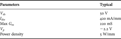
A gate pinch-off voltage V p (average value) of −2.2 V is characteristic of the Schottky contact. The breakdown limit voltage V BDs is above 200 V. The average power density is around 5 W/mm. Table 1 summarizes the main DC parameters of the recommended operating ratings of the technology.
Recommended operating ratings of GH50 technology.

Power bars have been manufactured based on the combination of unit-cell transistors. Thin film metallic resistors and active resistors based on the AlGaN sheet resistance are also used to stabilize transistors.
Based on all the previous work done up to now, the following quiescent bias point is used:
– V gs0 = −1.8 V (I dq = 25 mA/mm): deep class AB;
– V ds0 = 50 V.
C) Non-linear model of the transistor unit cell
The UMS GH50 non-linear transistor model is scalable and valid for multi-bias operation. The unit-cell transistor model represents eight fingers of 250 µm gate width. The non-linear model relies on both S parameter measurements and pulsed I(V) characteristic measurements. The non-linear elements considered in this model are the current sources as well as the gate-source and gate-drain capacitors. These elements are deduced from the pulsed I(V) and S parameter characteristics, obtained by excursion around the bias point using short voltage pulses. It includes also a dynamic thermal circuit. However, in order to alleviate the computation burden during the first steps of the amplifier design process, the dynamic thermal circuit can be deactivated and replaced by an isothermal model.
On the other hand, a power bar enables to reach the desired output power will be constructed by paralleling several unit-cell transistors with additional passive elements modeling the interconnections between all the transistors, and including the bonding wires.
D) Broadband multi-harmonic source-pull/load-pull simulations
Multi-harmonic (fundamental and second harmonic) source-pull and load-pull simulations have been performed in order to define the optimum source and load terminations to maximize PAE (PAE max) as a function of frequency. Constant PAE contours close to PAE max have been also extracted.
Figure 1 shows the optimum source impedance (Z S_UC_Opt) and the optimum load admittance (Y L_UC_Opt) to be presented to a unit-cell transistor in order to reach PAE max in the 1.0–4.5 GHz frequency range.
Optimum source generator impedance (a) and optimum load admittance. (b) for PAE max in the 1.0–4.5 GHz frequency range.

From Fig. 1, input and output equivalent circuits of a unit-cell transistor can be extracted at the fundamental frequency for the optimum operating point leading to PAE max.
Amazingly, these input and output equivalent circuits are very simple in the 1–4.5 GHz bandwidth.
– The input circuit results in a R in–C in series circuit, with R in = 3.5 Ω and C in = 6 pF;
– whereas the output circuit results in a R out–C out parallel circuit, with R out = 130 Ω and C out = 0.9 pF.
A detailed analysis of the simulations shows that the optimum source and load terminations at the fundamental frequency are not dependent, at least to first order, on the termination presented at the second harmonic.
In other words, the input and output matching circuit synthesis can be practically performed at the fundamental and second harmonic frequencies, independently.
E) Calculation of bandwidth limitation of maximum obtainable PAE: Bode–Fano limitations
For a given technology, optimum design of wideband and high-PAE amplifiers requires the knowledge of the limitation of the maximum obtainable PAE versus frequency. This theoretical limitation, calculated for a unit-cell transistor, is defined by the Bode and Fano theorems [Reference Bode5, Reference Fano6]. The application of these theorems consists, firstly in determining the equivalent electrical circuit of the transistor working in an optimized operating mode, as previously described in Section II.D.
Secondly, applying the integral limitations defined by Bode for a parallel RC circuit, and extended by Fano to more complex circuits, enables us to calculate the bandwidth limitations due to the input and output equivalent circuit of the unit-cell transistor.
In order to obtain closed forms of bandwidth limitations, Bode and Fano assumed constant reflection coefficients in the bandwidth of interest. The final relevant expressions are then the following:
– For the series R in–C in input circuit:
(1) $$\Delta f=\displaystyle{{2\pi ^2 R_{in} C_{in} f_0^2 } \over {{\rm ln}\left\vert {\displaystyle{1 \over {\Gamma _S }}} \right\vert }}\comma$$

where R in and C in are the elements of the input transistor circuit (Z in) extracted from source-pull measurements; f 0 is the central frequency of the operating bandwidth; ΓS is the reflection coefficient presented by the source impedance to the input transistor equivalent circuit Z in.
– For the parallel R out–C out output circuit:
(2)$$\Delta f=\displaystyle{{R_{out} C_{out} } \over {2\, {\rm ln}\left\vert {\displaystyle{1 \over {\Gamma _L }}} \right\vert }}\comma$$
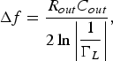
where R out and C out are the elements of the output transistor circuit (Z out) extracted from load-pull measurements; ΓL is the reflection coefficient presented by the impedance load Z L to Z out.
A comparison of the bandwidth limitations due to the input and output transistor circuits shows that the bandwidth is definitively limited by the output circuit.
In Fig. 1(b), constant PAE contours around PAE max extracted from the load-pull simulations show that in order to maintain PAE higher than 90% of PAE max, the magnitude of the load reflection coefficient ΓL(ω) is defined by
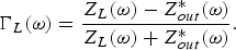 $$\Gamma _L \lpar \omega \rpar =\displaystyle{{Z_L \lpar \omega \rpar - Z_{out}^ \ast \lpar \omega \rpar } \over {Z_L \lpar \omega \rpar +Z_{out}^ \ast \lpar \omega \rpar }}.$$
On the other hand, Fano showed [Reference Fano6] that an optimized equal ripple Chebyshev matching circuit, with a finite number of lossless matching elements, can be designed as a function of the output time constant τ out = R outC out.
Figure 2 shows the reachable bandwidth plotted as a function of |ΓL|, parameterized by the element number of the lossless matching network.
Reachable bandwidth plotted for τ out=1.17 × 10⁻¹⁰ s, as a function of |ΓL|, parameterized by the element number of the lossless matching network.
It results that for τ out = 1.17 × 10⁻¹⁰ s, the maximum reachable bandwidth varies from 1.6 GHz (n = 2) to 2.7 GHz (n = ∞). It follows that to reach 90% of PAE max, the maximum theoretically attainable bandwidth is equal to 2.7 GHz.
Now, by taking into account output matching circuit losses, the magnitude of the load reflection coefficient must be lower than 0.2, in order to reach PAE higher than 90% of PAE max using a finite number of real elements.
During the synthesis of the output matching network with lossy elements, a trade-off has to be found between the insertion loss and the number of matching elements to maximize both bandwidth and PAE.
F) Constraint on the second harmonic frequency (H2) termination: Chalmers criterion
The Microtechnology and Nanoscience group of the University of Chalmers [Reference Saad, Fager, Cao, Zirath and Andersson7] proposed an efficient method to control carefully the second harmonic frequency (H2) termination in order to maintain a high overall PAE in wideband amplifiers.
While maintaining the optimum load impedance at the fundamental frequency, H2 impedance is varied across the periphery of the Smith Chart.
Figure 3 shows, for a unit-cell transistor, the simulation of the PAE as the function of the phase of the second harmonic reflection coefficient, while maintaining the optimum load impedance at the fundamental frequency.
Influence of the second harmonic ΓL(ω) on simulated PAE at 2, 3, and 4 GHz.
It can be noted that PAE is rather independent on the second harmonic phase except when it approaches the short-circuit region at the internal drain controlled-current source plane. This means that, during the design of the output matching network, no additional design efforts are needed for the second harmonic if the matching network does not approach the short-circuit region. Similarly, a critical H2 termination region must be avoided at the transistor input ports.
G) Determination of the input/output matching networks at the fundamental frequency under H2 constraint termination
A single-ended wideband (1–3 GHz) MIC and two wideband (2–4 GHz) Quasi-MMIC (single ended and balanced) HPAs GaN HEMT have been designed.
The first step consists in determining the source and load optimum impedances from unit-cell transistor source-pull (Z S_UC_Opt) and load-pull (Z L_UC_Opt) simulations.
Then, the output transformer-combiner of the power bar is synthesized in order to present to each unit-cell transistor the same optimized load impedances Z L_UC. Please note that Z S_UC and Z L_UC at the second harmonic frequency must fulfill the Chalmers criterion for high-PAE performance.
The third step consists in synthesizing the input transformer-divider of the power bar using the same method while the output of the power bar is loaded by the optimized output transformer-combiner.
Finally, a global EM fine tuning is performed before the layout realization. Non-linear stability analyses are realized at each design step.
1) WIDEBAND (1–3 GHZ) MIC HPA, EXTERNALLY MATCHED
A 12 mm GaN power bar device, made of six 8 × 250 µm GH50 unit-cell transistors, in ceramic package (CHK040A-SOA from UMS) has been used. The package transition has been simulated with 3D EM simulator. Input and output matching networks have been realized on Rogers RT6010 substrate (ε r = 10.2, h = 632 µm).
Figure 4 (top) shows the input and output distributed matching networks schematic. Figure 4 (bottom) shows photography of the realized 1–3 GHz MIC HPA.
Input and output distributed matching networks schematic (top) and photography of the fabricated wideband HPA (bottom).
Figure 5 shows the unit-cell transistor load impedances (Z L_UC) in the 1–6 GHz range (addressing fundamental and second harmonic frequencies) inside the HPA structure. It is compared with the unit-cell transistor optimum impedances (Z L_UC_Opt) obtained from load-pull simulations. In the 1–3 GHz range, the comparison shows that the results are very close to load-pull simulations. The resulting unit-cell transistor load impedances (Z L_UC) enable to obtain PAE higher than 90% of PAE max (as defined in Section II.D).
Optimum fundamental load impedance ZL_UC_Opt (black) and realized fundamental and H2 load impedance Z L_UC in simulation (green) of unit-cell transistor.
Figure 5 also presents the H2 impedance area to be avoided for a unit-cell transistor. Note that in the 2–6 GHz range, the unit-cell transistor load impedances (Z L_UC) are not in the H2 low PAE region.
Considering the previously defined PAE constraints, the input matching network has been designed to obtain a flat gain over the bandwidth. A low-frequency stabilizing circuit has also been added to the input matching network (Fig. 4) without damaging gain or PAE in the bandwidth.
The size of the amplifier prototype is 50 × 110 mm2 as shown in Fig. 4.
A comparison between measured and simulated performances of this MIC HPA will be presented in Section III.
2) WIDEBAND (2–4 GHZ) QUASI-MMIC SINGLE-ENDED HPA INTERNALLY MATCHED
A second single-ended amplifier, based on the same design methodology, has been realized with a passive GaAs MMIC circuit technology [Reference Camiade8]. Advantages of passive MMIC technology are high integration (low size of MMIC matching network) and high design flexibility (lumped and distributed elements). The last generation of this process called ULRC provides improved substrate isolation, higher MIM capacitor breakdown voltage (V bk_capacitor is higher than 200 V), and increased current density capability of the transmission lines.
A GaN power bar of 8 mm (4 × 8 × 250 µm) has been used for the design of this second single-ended PA. On top of providing compact solution, the integration of matching networks inside the package reduces the limitations due to the package transitions and eases the realization of wide band solutions. The output matching network has been designed by optimizing the PAE performances at both fundamental and second harmonic frequencies. It is synthesized in order to obtain a Chebychev band-pass response and implemented using lumped elements.
The input matching network design approach is similar to the first PA example; the main difference is the use of GaAs passive elements. It was designed as a 50 to 5 Ω Chebychev constant impedance transformer.
Thanks to the use of GaAs passive technology for matching; the integration of biasing network was possible and was introduced. This reduces significantly the overall size of the PA. The size of this internally matched amplifier is lower than 420 mm2.
Figure 6 shows the photography of the wideband single-ended Quasi-MMIC 25 W GaN power amplifier (PA).
Photography of single ended wideband Quasi-MMIC 25 W GaN HPA internally matched.
An output power higher than 25 W over 2–4 GHz bandwidth has been obtained. A comparison between measured and simulated performances of this Quasi-MMIC wideband single-ended PA will be presented in Section III.
3) WIDEBAND (2–4 GHZ) QUASI-MMIC BALANCED HPA, INTERNALLY MATCHED
A balanced wideband Quasi-MMIC HPA has also been designed based on two 25 W single-ended internally matched PAs. The design uses the same procedure as the one described previously.
The design of the balanced architecture is based on the use of Lange couplers (0°/90°) [Reference Arnous, Bathich, Preis and Boeck9]. These couplers are well known as very good matching power combiners/dividers over a large bandwidth due to the fact that the 0°/90° configuration makes naturally the return loss independent of both input and output reflection coefficients of the individual single-ended devices. The Lange couplers have been designed with microstrip line width and gap dimensions ensuring sufficient voltage and current handling capabilities. The Lange coupler length corresponds approximately to a quarter wavelength (λ/4) at the 3 GHz center frequency. Realized on GaAs substrate (ε r = 12.8), the microstrip line length of the optimized Lange couplers is very long (equal to 8652 µm), as shown in Fig. 7, and it was necessary to bend the structure. The unused port 4 is terminated with optimized 50 Ω resistor supporting maximum 1:2 standing wave ratio. The Lange couplers are connected to the input/output matching network with wires bonding.
Photography of the 0°/90° Lange coupler.
On wafer measurements of the test structure of the microstrip Lange coupler have been performed in a two-port 50 Ω environment with the unused port terminated by 50 Ω resistor. The simulated and measured through connection (S 31) and coupling factor (S 32) results of the coupler are compared in Fig. 8. Simulated and measured data show a good agreement.
Simulated and measured through connection (S 31) and coupling factor (S 32) of the Lange coupler.
Owing to the unequal S 31 and S 32 response of the wideband 0°/90° Lange coupler in the wide operating bandwidth, the upper and lower input (IMN1–IMN2)/output (OMN1–OMN2) matching networks (Fig. 9) are not identical in order to compensate this asymmetry. Note that the bounding wires have equal electrical length in the single-ended (25 W) and balanced PA (45 W).
Photography of the 45 W wideband (2–4 GHz) GaN balanced HPA.
Figure 9 shows the photography of the fully integrated 45 W wideband GaN balanced PA.
The wideband balanced internally matched HPA generates an output power higher than 45 W over the 2–4 GHz bandwidth. A more detailed comparison between measured and simulated performances of this wideband Quasi-MMIC balanced HPA will be presented in the next section.
III. COMPARISON BETWEEN SIMULATED AND MEASURED RESULTS
A) CW measurement results of the wideband (1–3 GHz) MIC HPA, externally matched
CW large signal measurements were performed at a drain voltage (V ds) of 50 V and quiescent current (I dq) of 300 mA. The measured and simulated results are presented in Fig. 10.
Simulated and measured large signal performances of the realized MIC HPA at V ds = 50 V, I dq = 300 mA for P av_generator = 36 dBm (PAEc Max).
The PA generates an output power higher than 45.8 dBm. The corresponding PAE is higher than 36% and the power gain (G P) is higher than 9.5 dB for an available power of the generator equal to 36 dBm. The measured and simulated results are in a good agreement in the 1–3 GHz frequency range.
B) CW measurement results of the wideband (2–4 GHz) Quasi-MMIC single-ended HPA internally matched
CW large signal measurements were performed at a drain voltage (V ds) of 50 V and quiescent current (I dq) of 200 mA. The measured and simulated results are presented in Fig. 11.
Large signal performances of the realized Quasi-MMIC single ended HPA at V ds = 50 V, I dq = 200 mA for P av_generator = 34.5 dBm (PAE Max).
The PA generates an output power higher than 44 dBm. The corresponding PAE (drain efficiency (DE)) ranges between 37 and 52% (40 and 55%) and the G P is higher than 9.8 dB for an available power of the generator equal to 34.5 dBm.
The measured and simulated results are in a good agreement in the 2–3.5 GHz frequency range. Above 3.5 GHz, a more accurate interconnections EM modeling analysis needs to be done.
C) Measurement results of the wideband (2–4 GHz) Quasi-MMIC balanced HPA, internally matched
This wideband balanced PA has been characterized in pulsed CW and with modulated signals.
1) PULSED CW MEASUREMENT RESULTS
The Quasi-MMIC balanced PA has been first characterized under CW small signal.
The measurements were performed at V ds = 50 V with V GS = −2 V and I dq = 400 mA. Figure 12 illustrates the comparison between the simulated and measured small signal gain, showing very good agreement over the frequency band.
Simulated (solid lines) and measured (dot lines) small-signal gain and input/output return losses versus frequency at V ds = 50 V and I dq = 400 mA.
Large signal measurements were also performed using a pulsed wave (250 µs/10%) input signal. Figure 13 reports the measured saturated output power, PAE, DE, and G P versus frequency.
Large signal performances of the realized HPA at V ds = 50 V, I dq = 400 mA for P av_generator = 37 dBm.
As shown in Fig. 13, a saturated output power ranging from 46.5 to 48.6 dBm over 2.0–4.0 GHz is obtained for an available power of the generator equal to 37 dBm. An associated minimum DE of 35% is achieved over the octave bandwidth.
The measured and simulated results are in a good agreement in the 2–3.5 GHz frequency range. Above 3.5 GHz, a more accurate interconnections EM modeling analysis needs to be done.
The performances of these wideband, high efficiency, HPAs, in the 1–4 GHz frequency range are among the best published results in terms of PAE, bandwidth, and output power trade-off.
2) TIME-DOMAIN LINEARITY MEASUREMENT RESULTS
In order to measure the linearity of GaN HPAs, a specific time-domain set-up has been developed. On the other hand, in order to improve the adjacent channel power ratio (ACPR), a simple first-order baseband digital predistortion (DPD) technique has been applied to the Quasi-MMIC balanced HPA.
Please note that our characterization set-up is not based on the measurement of the envelope of the modulated RF signal but on direct sampling of RF waveform acquisition.
A) Description of the wideband time-domain measurement set-up
A fully calibrated four-channel wideband time-domain measurement system is represented in Fig. 14 [Reference Ahmed, Neveux, Reveyrand, Barataud and Nebus10].
Block diagram of the four-channel wideband time-domain measurement set-up.
This wideband time-domain measurement system is based on track and hold amplifiers (THA). Broadband bidirectional couplers are used to simultaneously acquire voltage and current waveforms at both ports of the amplifier under modulated signal excitation. This sub-sampling RF measurement system enables to work with very high equivalent sampling frequencies and it allows a spectral resolution as high as 10 kHz over a 3 GHz instantaneous bandwidth.
Please note that the measurement set-up is configured to work at an 80 GS/s equivalent sampling frequency.
A 2.5 GHz carrier frequency is chosen. A 20 MSymb/s – 5.9 dB peak to average power ratio (PAPR) –0.35 roll-off – 16QAM modulation scheme has been applied to feed the device under test (DUT). The modulated signal is digitally calculated at a sampling frequency of 20 GS/s (a generator(t)). The digital data are then sent to the arbitrary waveform generator (AWG), working at a sampling rate of 20 GS/s. Owing to the 1 Vpeak–peak output voltage limitation of the AWG; the modulated RF signal is amplified with a linear driver whose output feeds the DUT.
B) Wideband multi-sine absolute calibration procedure
The set-up calibration procedure is detailed below since the validity of the linearity measurements is fully dependent on it.
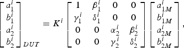
An accurate absolute calibration procedure for dense spectral components with a high resolution of 20 kHz is performed over a wide spectrum band (100 MHz) [Reference El-Akhdar, Ahmed, Neveux, Reveyrand, Barataud and Nebus11]. This wideband calibration procedure is based on the use of a multi-sine signal consisting of summation of sinusoids with constant amplitude and a Schroeder phase definition. This signal is then converted from digital to analog domain using the AWG. The first step of the calibration procedure, for connectorized DUT, consists in a relative error correction to compute the error coefficients described in equation (4). This relative calibration is performed using SOLT standards. To extract the error coefficients for all the spectral lines to be calibrated, a single measurement is made for each standard, reducing calibration time
 $$\left[{\matrix{ {a_1^i } \cr {b_1^i } \cr {a_2^i } \cr {b_2^i } \cr } } \right]_{DUT}=K^i \left[{\matrix{ 1 & {\beta _1^i } & 0 & 0 \cr {\gamma _1^i } & {\delta _1^i } & 0 & 0 \cr 0 & 0 & {\alpha _2^i } & {\beta _2^i } \cr 0 & 0 & {\gamma _2^i } & {\delta _2^i } \cr } } \right]\left[{\matrix{ {a_{1M}^i } \cr {b_{1M}^i } \cr {a_{2M}^i } \cr {b_{2M}^i } \cr } } \right]\comma$$
where i = 1, …, N and denotes the frequency index.
For absolute calibration the same signal measured by a calibrated digital sampling oscilloscope (DSO) is used as a reference leading to the set-up shown in Fig. 15.
Measurement set-up for absolute calibration.
The DSO that works on the coherent interleaved sampling principle is configured to acquire the signal at an equivalent high sampling rate. The acquired waveform is processed to de-embed the effect of the attenuator using their respective S-parameters.
Figure 16 describes the measurement results for the incident a 1(t) and transmitted b 2(t) voltage signals in through mode.
Calibrated incident a 1(t) and transmitted b 2(t) voltage waves at both reference planes for 20 MSymb/s 16QAM RF signal in through connection.
A very good coherence between the two signals is obtained. The amplitude and phase of the RF-modulated signal for the two waveforms, observed in the zoom of Fig. 15, is exactly the same validating the wideband multi-sine calibration procedure.
C) Linearity results
A simple first-order base band predistortion technique reported in [Reference Bacque12]. DPD is applied to the 50 W Quasi-MMIC balanced HPA. It is based on the linearization of the complex envelope  $\widetilde{b}_2 \lpar t\rpar $ extracted from the equivalent-time transmitted modulated RF voltage wave (real signal b 2(t)) over the digitally modulated and interpolated signal downloaded in AWG (real signal a generator(t)).
Figure 17(a) shows the equivalent-time incident (a 1(t)) and reflected (b 1(t)) modulated RF voltage waves and the associated magnitudes of the complex envelope  $\left\vert {\widetilde{a}_1 \lpar t\rpar } \right\vert $ and
 $\vert {\widetilde{b}_1 \lpar t\rpar } \vert $ calculated with Hilbert transform. It represents then the time-domain input reflection of the balanced Quasi-MMIC HPA. A zoom of these time-domain waveforms allows the visualization of the dynamic phase shift and the dynamic magnitude attenuation between a 1(t) and b 1(t).
Incident a 1(t), reflected b 1(t) (a) and transmitted b 2(t). (b) Voltage waves and associated envelope magnitudes at both ports of the HPA for an excitation with a 20 MSymb/s 16 QAM RF signal with DPD.
Figure 17(b) shows the equivalent-time incident (a 1(t)) and transmitted (b 2(t)) modulated RF voltage waves and the associated magnitudes of the envelope  $\left\vert {\widetilde{a}_1 \lpar t\rpar } \right\vert $ and
 $\left\vert {\widetilde{b}_2 \lpar t\rpar } \right\vert $. It represents then the time-domain dynamic transmission of the balanced Quasi-MMIC HPA. A zoom of this time-domain waveforms allows the estimation of the dynamic gain and group delay of this HPA.
Figure 18 shows the measurement results of the dynamic AM/AM and AM/PM characteristics of the HPA before and after digital memoryless predistortion for P av_generator = 31.4 dBm.
Measured dynamic AM/AM and AM/PM characteristics of the amplifier at V ds = 50 V, I dq = 400 mA for P av_generator = 31.4 dBm driven with a 20 MSymb/s 16QAM modulated signal with digital memoryless predistortion.
Please note that the output of the HPA follows a linear behavior when the DPD is applied.
Figure 19 shows the corresponding power spectrum (without any averaging process) at the output of the HPA before and after memoryless DPD. On the other hand, it can be shown that thanks to our direct sampling of RF waveform acquisition, a very high-resolution spectrum of the output voltage wave b 2(t) of the balanced Quasi-MMIC HPA is obtained. The measurement of this 20 MSymb/s 16QAM modulated signal requires at least a 100 MHz instantaneous bandwidth. This value is close to the instantaneous bandwidth limitation of commercially available vector signal analyzers. Higher instantaneous bandwidths (3 GHz with10 kHz resolution for instance) can be easily reached with the time-domain set-up based on THAs
Measured RF spectrum at the output of the HPA at V ds = 50 V, I dq = 400 mA driven with a 20 MSymb/s 16QAM modulated signal with and without digital memoryless predistortion.
Figure 19 demonstrates that a 10 dB improvement of ACPR is achieved. Same improvement results are also obtained at 3 and 3.5 GHz.
The results clearly show that the implemented HPA in cooperation with a simple linearization technique can linearly amplify the various modulated signals over the various operating frequencies.
IV. CONCLUSION
In this paper, the design procedure, advanced realization, and characterization of wideband, high efficiency, HPAs have been presented. The design approach is based on a theoretical study of the performance limitations of the “efficiency-bandwidth” trade-off derived from the Bode–Fano integrals, applied to actual lossy networks. The proposed method is validated through the implementation of three HPAs:
– a single-ended 1–3 GHz MIC externally matched HPA. It generates an output power greater than 40 W with a G P higher than 9.2 dB and a PAE higher than 36% over the bandwidth;
– a single-ended 2–4 GHz Quasi-MMIC internally matched HPA. It generates an output power greater than 25 W with a G P higher than 9.8 dB and PAE (DE) between 37 and 52% (40 and 55%);
– a balanced 2–4 GHz Quasi-MMIC internally matched HPA. The output power is greater than 45 W with a G P higher than 9.5 dB and PAE higher than 38% over the bandwidth.
These HPAs address the needs for current and future active phased-array radar applications, countermeasures, and warfare.
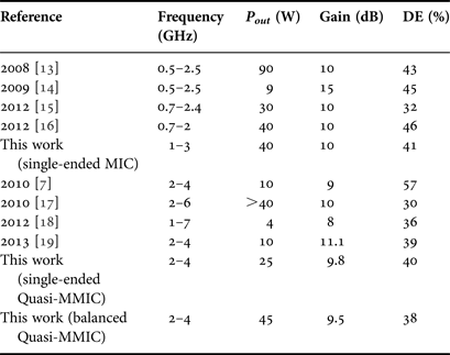
Table 2 summarizes some recently published performances of wideband GaN PAs working with a:
– 3 GHz maximum operating frequency (upper part),
– 4–7 GHz maximum operating frequency (bottom part).
As shown in Table 2, results presented are among the best results published in terms of trade-offs between output power and PAE performances for wideband HPAs in the 1–4 GHz frequency range.
Performances of wideband (higher than 1 octave) high PAE GaN PAs with a maximum operating frequency of 3 GHz (top table) and 7 GHz (bottom table).
ACKNOWLEDGEMENT
Professor Juan Obregon from Xlim Laboratory is gratefully acknowledged for helpful discussions.
Chamssedine Berrached was born in Angoulême, France, in 1986. He received the M.S. in Electrical, Electronics and Microwave Engineering from the University of Limoges, France, in 2009 and is currently working toward the Ph.D. degree at Xlim laboratory, Limoges, France in partnership with United Monolithic Semiconductors, Villebon-sur-Yvette, France. His research concerns the design of high efficiency and wideband HPAs.
 Kassem El-Akhdar was born in Nabatieh, Lebanon, in 1986. He received the master degree from the University of Limoges, France, in 2010. Currently, he is pursuing Ph.D. in Electronics at the University of Limoges. His research interests include the time-domain non-linear characterization of RF and microwave devices and systems.
 Diane BOUW received the M.S. degree in Microwave and Optic Communications in Engineering from the Research Institute of Microwave and Optical Communications of the University of Limoges (IRCOM, Limoges, France), in 2005. She joined UMS in 2005 as a Design Engineer of MMIC components, where she worked on high-power amplifier and non-linear stability for several applications. Since 2009, she is an Advanced Product Designer Engineer on the high-power transistor business line and participates in the development of the hybrid product based on GaN components for high power.
 Marc Camiade received the Dpl. Eng. degree in Physics and Electronic Engineering from the Institut National des Sciences Appliquées, Toulouse, France, in 1981. He joined Thomson-CSF in 1982 as a Design Engineer of hybrid circuits, where he participated in a variety of microwave and millimeter-wave circuits. Since 1988, he has been Application Group Manager in charge of new product development based on MIC and MMIC components. He joined United Monolithic Semiconductors in 1996, in charge of the development of MMIC components for Defense, Automotive, and Telecommunication applications. Since 2009, he is in charge of all the UMS advanced developments on new millimeter-waves and high-power technologies. He is also responsible for the new business line “GaN Power Transistors”.
 Denis Barataud was born in Saint-Junien, France, in 1970. He received the engineer's degree from the Ecole Nationale Supérieure de Télécommunications de Bretagne, Bretagne, France, in 1994, and the Ph.D. degree in Electronics from the University of Limoges, Limoges, France, in 1998. From 1998 to 1999, he was a Postdoctoral Scientist with the Microwave Laboratory, CNES, Toulouse, France. Since 2000, he has been with the XLIM (formerly IRCOM) Laboratory, University of Limoges, where in 2001 he became an Assistant Professor. His research interests include the development of time-domain equipment and techniques for the characterization of non-linear devices.
 Guillaume Neveux was born in Civray, France, in 1976. He received the Diplôme d'Etudes Approfondies (DEA) degree from the Université Paris 11, Orsay, France, in 2000 and the Ph.D. degree in Electronics and Communications from the National Superior Institute of Telecommunications (ENST), Paris, France, in 2003. Since 2004, he has been with the instrumentation group of the XLIM Laboratory at the University of Limoges (France). His research interests include the non-linear measurement with LSNA, and the study of RF sampling system.