Introduction
Dielectric thin films of high- and low-refractive index are the essential building blocks for optical coatings.[Reference Macleod1] Common low-refractive-index films are silicon oxide (SiO2, n ~ 1.54) and magnesium fluoride (MgF, n ~ 1.27); and high-refractive-index films include titanium oxide, zinc oxide, and silicon nitride (n ~ 2.0). Two sputtering techniques are widely used to deposit dielectric thin films.[Reference Pliskin2] For the highest density films, radio-frequency (RF) sputtering of pure oxide ceramic targets is normally preferred.[Reference Hanaizumi, Ono and Ogawa3–Reference Kitao, Imakita, Kawamura and Fujii9] For large area coating at high rates, reactive sputtering using element or alloy targets via direct current (DC) power supplies is the most common method.[Reference Rademacher, Bräuer, Fritz and Vergöhl10–Reference Pernice, Xiong and Tang12] Although RF sputtering results in high-quality films, it has the limitation of relatively low deposition rates. DC reactive sputtering from metallic targets has higher deposition rates but typically results in lower-quality films. In addition, there is a fundamental process stability problem due to oxide poisoning of the target surface when planar targets are used in DC reactive sputtering.[Reference Kuschel and von Keudell13–Reference Strnad, Jakab-Farkas, Papp, Fekete, Biro and Vida-Simiti17]
The ideal sputtering process of dielectric thin films would combine the high rates of reactive sputtering with the film quality and process stability of RF sputtered films. Toward this goal, the authors have developed novel conductive ZnO:Zn[Reference Zhou, Dubey, Simões, Fan and Neto18] and SiO2:Si composites to achieve high-rate sputtering deposition of high-quality dielectric films with high- and low-refractive index.
In this paper, the authors present the sputtering characteristics of the conductive SiO2:Si and ZnO:Zn composites in DC and RF plasma discharge. The optical properties of the resulting SiO2 and ZnO films are compared with RF sputtered films from the corresponding pure oxide targets. The SiO2:Si and ZnO:Zn composite targets are sputtered for a prolonged period to verify the process stability, i.e. whether or not the target poisoning occurs. The authors also discuss the mechanisms that enable much higher sputtering deposition rates from the SiO2:Si and ZnO:Zn composites than from quartz and pure ZnO targets.
Experimental details
Standard ceramic process was used to prepare the SiO2:Si and ZnO:Zn composite compacts. The process included mixing the oxide powder with corresponding element powder, high-pressure pressing of mixed raw materials into tablet, and sintering in Ar at temperatures from 500 to 1450 °C. Small size pellets with 10 mm diameter and 5 mm thickness were prepared at the initial materials investigation stage. Then composite targets with selected composition were prepared and used for the sputtering experiments. The targets were 50.8 mm in diameter and ~3.2 mm thick.
The SiO2:Si composite compacts were prepared using SiO2 and Si powders. Reagent SiO2 powder was from Alfa Aesar (99.5% in purity). The Si powder was prepared from crushing and then grinding doped Si bulk materials that had a resistivity of 1~5 Ω.cm. The compositions studied were expressed as (1−x)SiO2 + xSi, where x was a ratio in weight and varied from 0% to 100%. The ZnO:Zn composite compacts were prepared using reagent ZnO and metal Zn powders of 99.99% purity from Alfa Aesar. The compositions studied were expressed as (1−x)ZnO + xZn, where x was a ratio in weight.
The sputtering source was a circular planar magnetron of 50.8 mm diameter. Prior to each sputtering deposition, the vacuum chamber was pumped down to a base pressure lower than 5 × 10⁻⁶ Torr. High-purity argon and oxygen were used as process gases and their flow rates were regulated by mass flow controllers. When the oxygen ratio was varied, the Ar flow rate was changed accordingly to maintain a constant pressure of ~4 mTorr. Two types of sputtering power supplies were employed: an Advanced Energy MDX DC power supply and a Dressler 13.65 MHz RF power supply. The SiO2 films were deposited at room temperature and the ZnO films were deposited at 180 °C. The substrates were soda lime glass of 0.7 mm thickness. For comparison, commercial targets of the same dimensions (50.8 mm diameter and 3.2 mm thickness) were used for sputtering deposition of SiO2 and ZnO films. These targets included boron-doped silicon, quartz, metal Zn, and ceramic ZnO, which were purchased from Kurt J. Lesker.
The microstructures of the composites were characterized using a Rigaku ROTAFLEX rotating anode X-ray diffraction (XRD) system. Energy-disperse spectroscopy (EDS) equipped within a Hitachi S-3400N scanning electron microscope system was used to analyze the composition of the composites. The transmittance and film thickness were measured using a Filmetrics spectrophotometer and a Dektak 150 profiler, respectively.
Result and discussion
First, systematic studies were conducted to identify the proper sintering temperatures. For (1−x)ZnO + xZn in the composition range of x = 20% to 60%, the composite density increased with the sintering temperature, reaching a maximum value of ~85% of theoretical density at ~800 °C. Further increasing the sintering temperature led to a decrease in the composite density. This density variation at high temperatures was due to the vaporization of Zn. The percentage to the theoretical density is the ratio of measured density to the theoretical density of the composite. The theoretical density of 80%ZnO + 20%Zn was calculated by 80% × 5.6 g/cm3 + 20% × 7.14 g/cm3, where 5.6 and 7.14 g/cm3 are the theoretical density of ZnO and Zn, respectively.
The density of the sintered SiO2:Si compacts increased with the temperature and became almost saturated after 1300 °C. At 1300 °C, a density >92% of theoretical value was obtained for the compact with composition ranging from x = 20% to 50%. As will be shown later, both SiO2:Si and ZnO:Zn composites became conductive once the Si or Zn weight percent was higher than about 20%. The desired composite targets would have low concentration of silicon or zinc, but be sufficiently conductive. Therefore, the composites with composition in the range of x = 20%–50% were of particular interest.
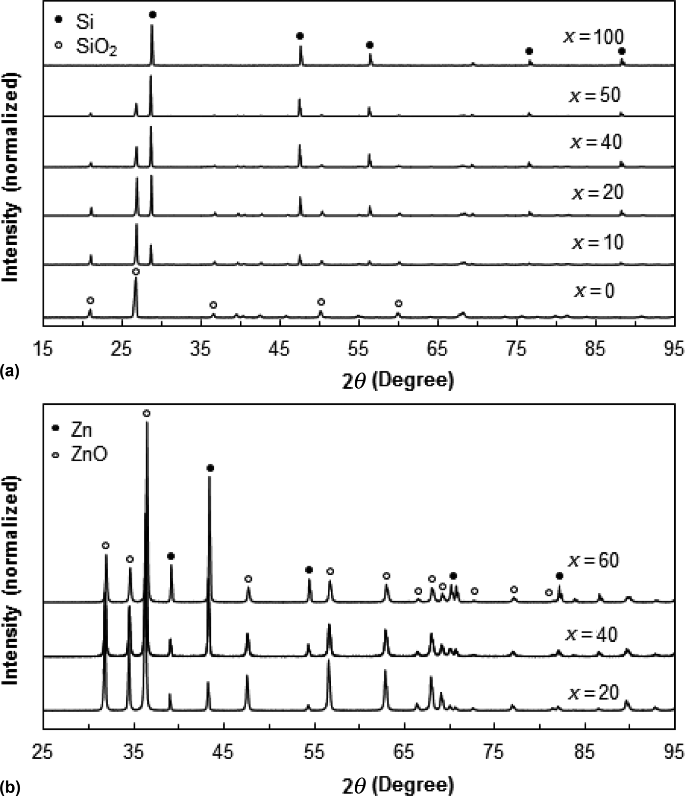
Figures 1(a) and 1(b) show XRD analysis results of the SiO2:Si and ZnO:Zn composites sintered at 1300 and 800 °C, respectively. Two primary phases co-existed in these composites: Si and SiO2, Zn, and ZnO. The amount of the Si or Zn phase increased with the x value, as expected. The results implied that the Si or Zn in the composition was not undergoing significant degree of oxidation during the sintering.
XRD patterns of sintered composites: (a) (1−x)SiO2 + xSi and (b) (1−x)ZnO + xZn.

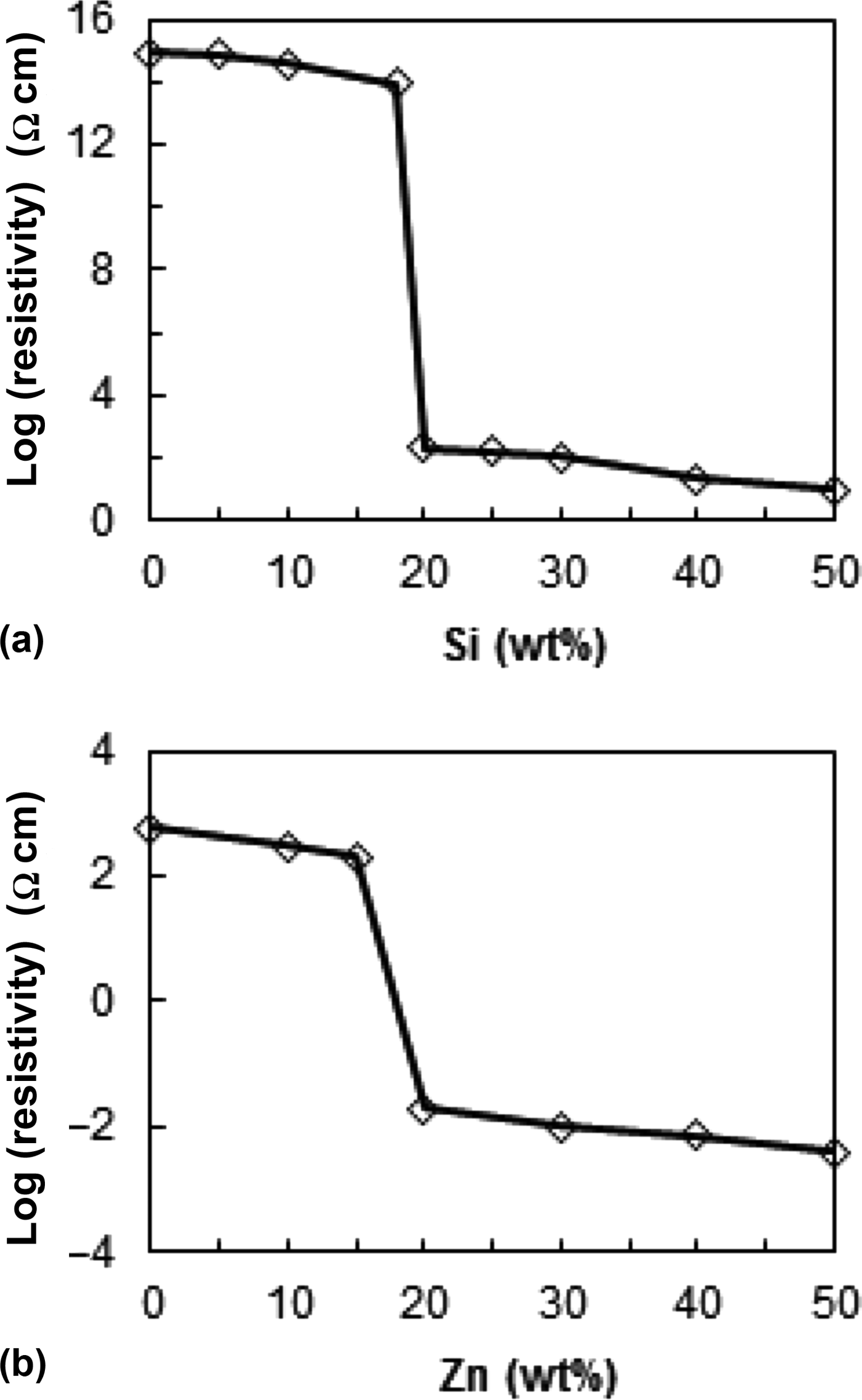
Figure 2 illustrates the room-temperature resistivity for the studied composites. The sintered ZnO appeared a semiconductor with resistivity of the order of 102 Ω.cm. For the ZnO:Zn composites, the resistivity decreased slightly as the x value increased from x = 0 to 0.2. A dramatic drop about four orders occurred at x ≥ 0.2 and then the resistivity decreased slightly with further increase in metal Zn concentration. Similar behavior was noted for the SiO2:Si composite. When the Si weight percent reached ~20%, the resistivity of the composite dropped suddenly from 9 × 10¹³ Ω.cm to about 200 Ω.cm. The abrupt change in the resistivity with increasing Zn or Si amount is believed to be caused by the formation of infinitive conductive path according to the percolation theory.[Reference McLachlan, Blaszkiewicz and Newnham19]
Resistivity dependence on x values for the sintered composites: (a) (1−x)SiO2 + xSi and (b) (1−x)ZnO + xZn.
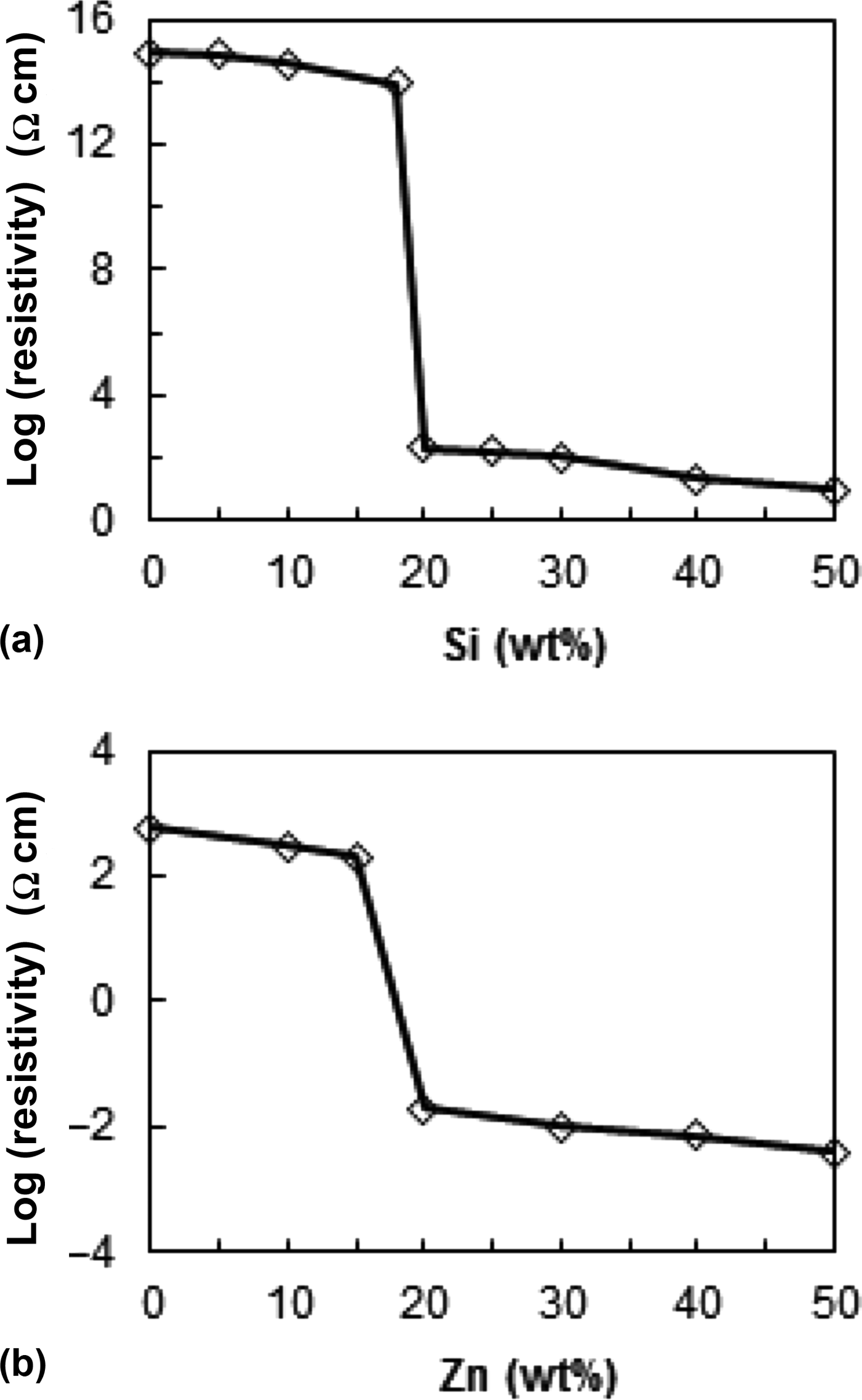
Based on the percolation theory, when the conductive particles are dispersed into a non-conductive matrix and the amount of the conductive phase increases from zero up to a critical volume fraction of percolation, one particle contact with neighbors and form finite conductive path where the host material is non-conductive. Near the critical volume, a conductive network is formed and the resistivity of the entire composite abruptly decreases. The obtained results appeared in good agreement with the percolation theory. The critical fraction of the conductive phase, doped-silicon, or metal zinc, was ~20% in weight in the current study.
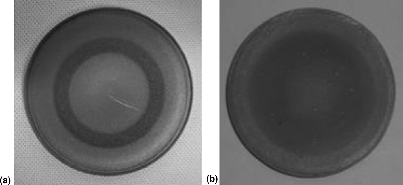
SiO2:Si and ZnO:Zn sputtering targets were fabricated with Si and Zn concentrations that made the composites sufficiently conductive. The results presented here were obtained from the SiO2:Si and ZnO:Zn targets with x = 40% Si or Zn, respectively. Other composition targets with x = 30% and 50% showed similar behaviors. Figure 3 are images of the SiO2:Si and ZnO:Zn targets after sputtering.
Images of sintered (a) SiO2:Si and (b) ZnO:Zn targets, which are ~50.8 mm diameter.
Figure 4 illustrates the dependence of the discharge voltage on the oxygen flow rates in DC sputtering of the composites and element targets. The silicon and metal Zn targets exhibited the typical sudden drop in the discharge voltage as the O2 flow increased to ~20% and ~30%, respectively. This was a typical effect in reactive sputtering due to the oxidation of the target surface, which led to stronger emission of secondary electrons than that from the element targets.
DC discharge voltage dependence on the O2 flow for (a) SiO2:Si and Si targets, and (b) ZnO:Zn and Zn targets. Note that the DC sputtering power was kept constant for each pair of targets. When the O2 flow was increased, the Ar flow was decreased to maintain the gas pressure at 4 mTorr.
On the other hand, increasing oxygen flow rates had only a little effect on the discharge voltage. The results indicated that the SiO2:Si and ZnO:Zn composite targets did not exhibit noticeable effect of target oxidation. Note that EDS analysis confirmed that the Si and Zn concentrations in the composites nearly did not change after the sintering. These results implied that the SiO2:Si and ZnO:Zn composite targets were not simply mixtures of SiO2 and Si or ZnO and Zn. In addition to forming infinitive conductive path, sub-oxides were likely formed, which need further confirmation.
The composite targets led to highly stable sputtering processes. With 30% oxygen flow, the SiO2:Si and ZnO:Zn targets were sputtered under DC power for over 240 min. No target-poisoning effect was observed, as the discharge voltage nearly did not change and no arcs were recorded from the power supply. Note that 30% oxygen flow was sufficient to produce fully oxidized films. Thus, using the composite targets effectively eliminated the stability issue of DC reactive sputtering.
In general, the quality of dielectric films produced by RF sputtering is superior to that produced by DC sputtering. The challenge is to increase the RF deposition rates. Figure 5 compares the deposition rates of SiO2 films RF sputtered from the SiO2:Si, Si, and quartz targets, and the deposition rates of ZnO films from the ZnO:Zn, Zn, and ZnO targets. Unexpected, the SiO2:Si target yielded a deposition rate about 4.9X and 1.9X higher than quartz and Si targets, respectively. The ZnO:Zn composite target also yielded ~40% and 18% higher deposition rates than ZnO and metal Zn targets, respectively. Similar increase in the deposition rates was also observed in DC sputtering. Thus, the composite targets are advantageous in terms of high-rate deposition.
Comparison of RF sputtering deposition rates of (a) SiO2 films from Si, quartz, and SiO2:Si targets, and (b) ZnO films from Zn, ZnO, and ZnO:Zn targets. The RF sputtering power was 40 W.
The high sputtering yields from the SiO2:Si and ZnO:Zn targets may be due to the difference in the kinetic-energy transfer that occurs in the composites compared with the pure oxide or element targets. The energy of ions striking the target surface of the pure oxides (quartz and ZnO) and elements (Si and Zn) can be effectively dissipated in materials that consist of uniform single phase (e.g., crystalline Si or quartz). In the case of the SiO2:Si and ZnO:Zn composites that consist of mixed phases, the interface between the two different phases may act as a barrier for energy dissipation. As a result, the kinetic energy of the sputtering ions is localized in a small region on the surface, leading to higher sputtering yield than that of single-phase target. Understanding the mechanisms of the high deposition rates of the composite targets is an interesting topic that needs further study.
High deposition rates and stable processes of dielectric films are very useful benefits for optical coatings and optoelectronic devices only if the resulting films have properties equivalent to those obtained from RF sputtering of the pure oxide targets. Figure 6(a) shows the transmittance spectra of the SiO2 films prepared from RF sputtering of SiO2:Si, Si, and quartz targets. The RF sputtering power was 40 W and the oxygen flow ratio was 20%. The SiO2 films were highly transparent and had nearly no difference in terms of optical transmittance. Analyzing the SiO2 films deposited on an accompanying wafer indicated that the film refractive index was about 1.44–1.49 at 550 nm. Figure 6(b) shows the transmittance spectra of the ZnO films prepared by RF sputtering from ZnO:Zn, Zn, and ZnO targets. The RF sputtering power was 40 W and the oxygen flow ratio was 30%. The ZnO films prepared from the ZnO:Zn target was as transparent as the film prepared from the pure ZnO. The high transmittance implied that these ZnO films were almost fully oxidized. Analyzing the films using Filmetrics indicated that the ZnO refractive index was in the range of 1.92–1.98 at 550 nm. The absorption edge was at ~378 nm, corresponding to an optical band gap ~3.28 eV, which is a common value for high-quality ZnO films.[Reference Bachari, Baud, Amor and Jacquet20–Reference Ellmer22] Note that, during the sputtering of the SiO2:Si and ZnO:Zn targets, sufficient oxygen flows were supplied and the deposition temperature was 180 °C. Under these conditions, oxygen vacancies in these films were suppressed to such a level that the SiO2 and ZnO films appeared highly transparent even without post-annealing. Of course, 180 °C was unlikely the optimum temperature and the oxygen flow ratio could be further reduced to obtain highly transparent ZnO films.
Optical transmittance spectra of RF sputtering deposited (a) SiO2 films from SiO2:Si, Si, and quartz targets, and (b) ZnO films from ZnO:Zn, Zn, and ZnO targets.
The results achieved through this research may be extended to other composite targets, e.g. Cr2O3:Cr and Al2O3:Al. Therefore, this study has the potential to significantly promote the manufacturing efficiency of optical coatings. In addition to optical coatings, SiO2 and ZnO thin films are widely used in optoelectronic and semiconductor devices, such as flat panel displays and field effect transistors. Similar to other sputtered ZnO films, the as-deposited polycrystalline ZnO films from the ZnO:Zn composite target were expected to be n-type. Clarifying the electrical properties of these ZnO films needs further research.
Conclusions
The SiO2:Si and ZnO:Zn composites become conductive once the doped silicon and metal Zn reach a critical ratio. Targets made of these composites can be sputtered using DC or RF power supplies to deposit low- and high-refractive index SiO2 and ZnO thin films. The target poisoning problem is eliminated in reactive sputtering of these composites. RF sputtering from the SiO2:Si and ZnO:Zn target yields deposition rates higher than sputtering from corresponding pure oxide and element targets. The quality of the RF sputtered SiO2 and ZnO films from the composite targets is comparable with the films obtained from RF sputtering of pure oxide targets in terms of optical transmittance. Using the composite targets has the potential to greatly promote the manufacturing efficiency of optical coatings.
Acknowledgments
The authors acknowledge support from FCT Portugal Grant No. PTDC/CTM-CER/121440/2010 and PEst-C/EME/UI0481/2013. This research was partly supported by National Science Foundation award no. 1462389 and South Dakota BOR PIF Grant.