Introduction
The focus of scientific research within the past decade has shifted to the investigation of the material behavior at the nanoscale. The proliferation of researchers studying materials on this length scale has resulted in the invention of the phrase “nanotechnology”. Meanwhile, studies of mechanical properties on this scale have led to the term “nanomechanics”, which is a subfield of mechanics characterizing the mechanical behavior of materials at atomic level subject to different types of boundary conditions.[ Reference Liu, Karpov and Park 1 ] As almost all mechanical properties of materials are temperature-dependent, small-scale characterization at high temperatures could lead to substantial opportunities in nanomechanics to understand material behavior at service temperatures and conditions relevant to industrial applications.[ Reference Beake and Smith 2 ] Accordingly, high-temperature nanomechanical testing techniques, predominantly high-temperature nanoindentation, are becoming increasingly popular among researchers within the nanomechanics community. The simplicity of the sample requirement, automated data collection and analysis, as well as the capability to probe small-scale physical phenomena in materials, such as dislocation nucleation, shear band activation, and phase transformations, have made high-temperature nanoindentation a powerful tool for small-scale materials characterization at elevated temperatures.[ Reference Wheeler, Armstrong, Heinz and Schwaiger 3 ] On the other hand, regardless of the specimen size, reliable high-temperature characterization calls for precise application and measurement of deformation (load or displacement) while concurrently controlling and measuring sample temperatures. Fundamentally, instrumented high-temperature nanoindentation requires additional instrumentation advances in two fields: (i) minimizing or eliminating oxidation and (ii) successful management of thermal drift and noise.[ Reference Kang, Merrill and Wheeler 4 , Reference Trenkle, Packard and Schuh 5 ] Procedures for satisfying these requirements have been discussed in the literature. These include works by Wheeler and co-workers[ Reference Wheeler, Armstrong, Heinz and Schwaiger 3 , Reference Wheeler, Brodard and Michler 6 , Reference Wheeler and Michler 7 ] and those brought forward by Schuh and his colleagues.[ Reference Trenkle, Packard and Schuh 5 , Reference Schuh, Packard and Lund 8 – Reference Schuh, Mason, Lund and Hodge 10 ] For the sake of brevity, they are not elaborated in this paper and interested readers are referred to relevant publications to comprehend the high-temperature nanoindentation instrumentations.
In this review, we systematically describe the influence of temperature on the mechanical behavior and corresponding plasticity mechanisms involved in nanoscale deformation of various materials subject to high-temperature nanoindentation loading. Our review provides an in-depth understanding of the mechanisms of surface plasticity at high temperatures where the interactions between thermal activation processes and surface stresses multiply the defect formation and nanoscale effects accompanied by the macroscopic mechanisms. In the remainder of this paper, thermally-activated deformation mechanisms in crystalline and non-crystalline materials under indenter, e.g., dislocation processes, shear transformation zone (STZ), and phase transformations, are elaborated; then the way to correctly measure mechanical properties of materials at high temperatures is explained and mechanical response of materials at elevated temperatures is discussed; research challenges and future directions in the field of high temperature nanoindentation are outlined in the last section of the paper.
Nanoscale deformation mechanisms
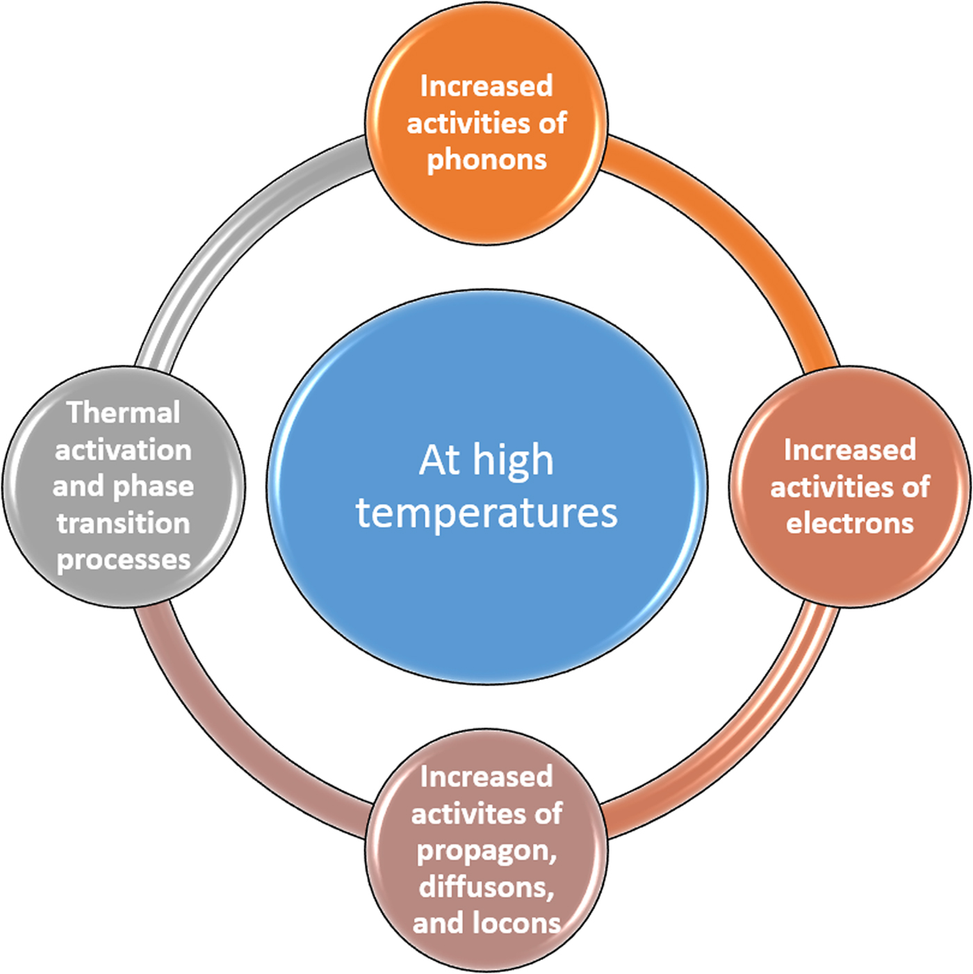
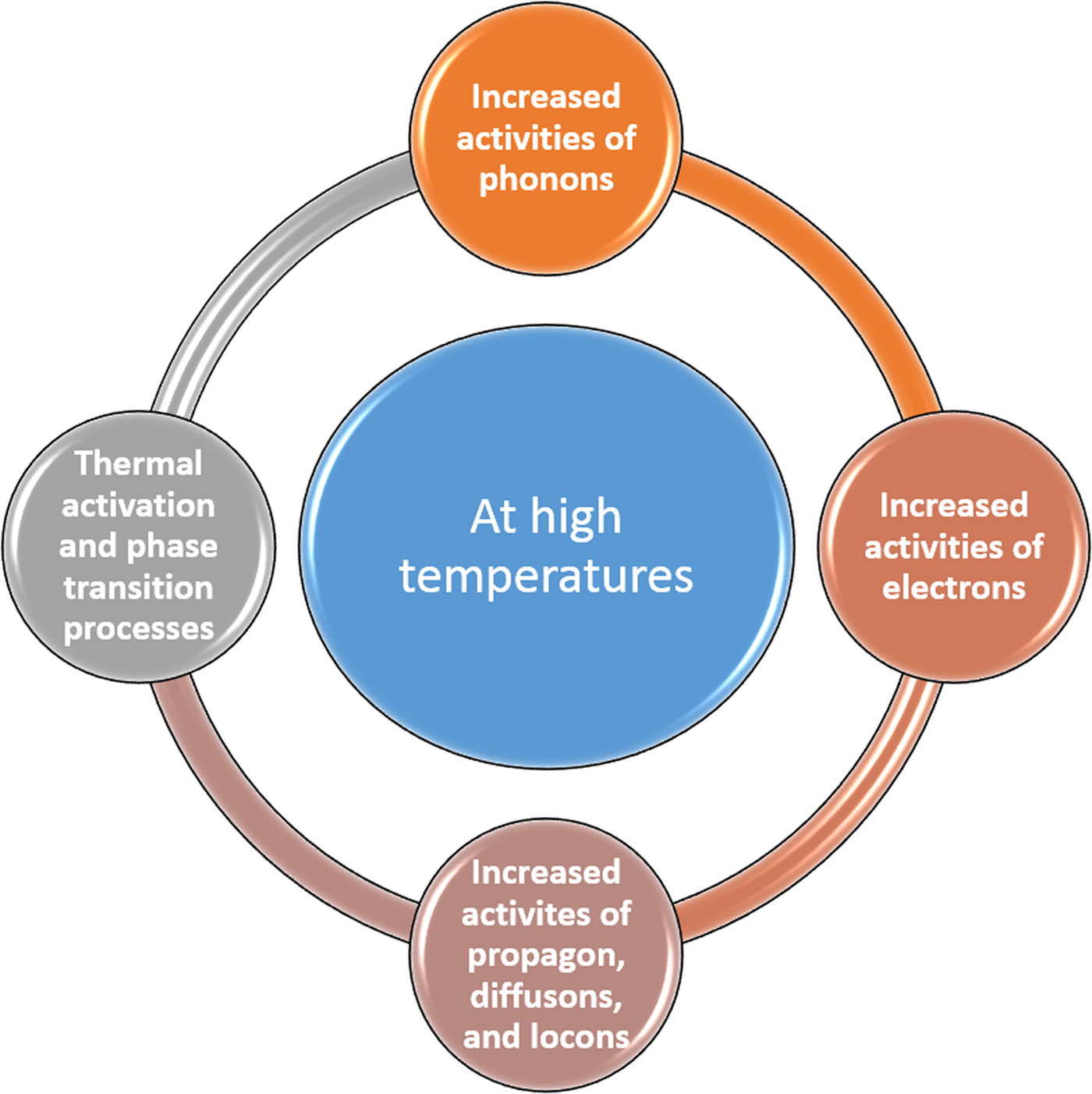
Heat content plays a crucial role in the deformation of microstructures and onset of nanoscale plasticity. As shown in Fig. 1, an increase in temperature leads to increased activities of phonons (in crystalline insulators and some semi-conductors), electrons (in metal and some semi-conductors), propagons, diffusons, and locons (in amorphous non-metallic materials),[ Reference Wingert, Zheng, Kwon and Chen 11 , Reference Hopkins, Ding and Poon 12 ] which in turn contribute to additional atomic displacements, an increase in the average interatomic distance, and a decrease in the restoring forces due to thermal expansion.[ Reference Chavoshi, Goel and Luo 13 – Reference Chavoshi and Luo 16 ] While increasing the dislocation mobility, a higher temperature lowers the minimum stresses required for homogeneous dislocation nucleation, dislocation gliding in a lattice, and breaking dislocation locks. As a result, thermal softening improves the plasticity of the material.[ Reference Chavoshi, Xu and Luo 17 , Reference Chavoshi and Luo 18 ]
Temperature-dependent phenomena in materials during high-temperature nanoindentation.
In the following, we focus on the insights provided by the high-temperature nanoindentation into the thermally-activated processes, activation energies, volumes, and the onset of plasticity. First, the plasticity of crystalline materials, primarily the thermally-activated dislocation processes, is discussed. Plasticity of non-crystalline materials is then covered, where the STZ mechanisms beneath the indenter at high temperatures are elaborated. Finally, a section is devoted to the phase transformation during nanoindentation at elevated temperatures.
Plasticity of crystalline materials
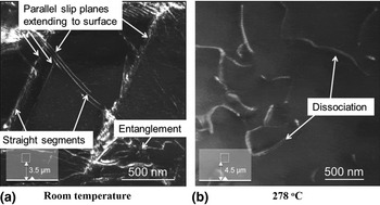
Thermally-activated dislocation plasticity in crystalline materials can be examined by high temperature nanoindentation experiments. Dark-field transmission electron microscopy (TEM) images of Mg17Al12 underneath the indentation shown in Fig. 2 indicate that at room temperature, dislocations are straight and mostly gliding on particular parallel slip planes extending to the surface with increasing dislocation entanglement towards the center of the plastic zone. At high temperatures, e.g., 278 °C, more homogeneous dislocation distribution is achieved, exhibiting a curved shape with some dissociation.[ Reference Mathur, Maier-Kiener and Korte-Kerzel 19 ]
Dark-field TEM of the indentation imprint on Mg17Al12. More homogeneous dislocation distribution exhibiting a curved shape with some dissociation is seen at the high temperature. Adopted with permission from Ref.[Reference Mathur, Maier-Kiener and Korte-Kerzel19] (Elsevier, 2016).

Nanoindentation tests of the two-phase eutectic Sn-Bi alloy up to 100 °C reveal that the dislocation climb controlled by core diffusion and power-law breakdown, in which the deformation is governed by dislocation glide-controlled flow, are the dominant creep and deformation mechanisms, respectively.[ Reference Shen, Wu, Wang and Chen 20 ] Dislocation climb motion controlled by the dislocation pipe mechanism is reported to be the creep mechanism of the bulks of low-Ag Cu/Sn-Ag-Cu-Bi-Ni/Cu microsolder joints up to 85 °C.[ Reference Kong, Kong, Sun, Sun, Yang, Yang, Liu and Liu 21 ]
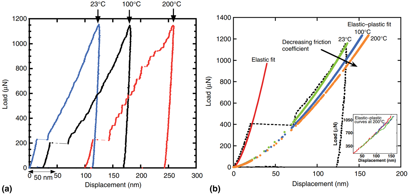
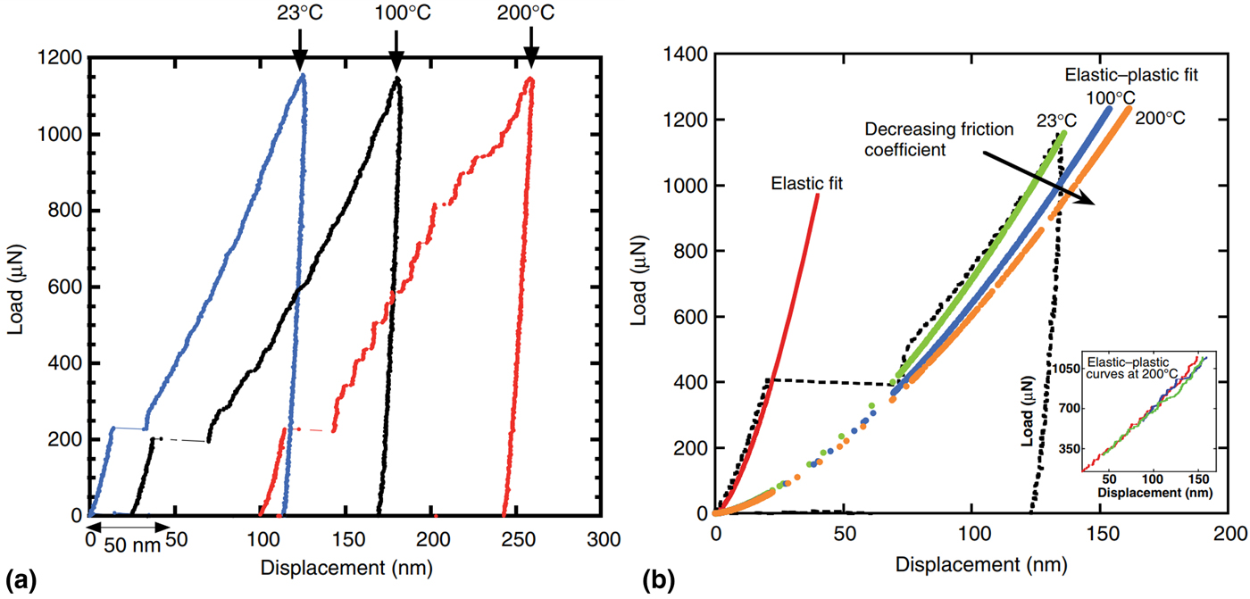
The occurrence of “pop-in” events in nanoindentation, i.e., sudden depth excursions under load control or sudden load drops under displacement control, is associated with the dislocation activity. As illustrated in Fig. 3(a), at room temperature, one large discontinuity is observed on the load-displacement (P-h) curves, whereas at 200 °C, multiple pop-ins separated by elastic reloading segments occur, resulting in a highly serrated P-h curve.[ Reference Rajulapati, Biener, Biener and Hodge 22 , Reference Franke, Alcalá, Dalmau, Duan, Biener, Biener and Hodge 23 ] The serrated flow behavior is a result of the defect evolution owing to the special quasi-elastic reloading. On the other hand, thermally-activated deformation processes, e.g., dislocation nucleation or abrupt release of dislocation entanglements causes the appearance of multiple pop-ins and discontinuity. Note that the Taylor dislocation model[ Reference Taylor 24 ] can be adopted to determine the temperature effects on the friction stress of screw dislocations.[ Reference Durst, Backes, Franke and Göken 25 – Reference Qiu, Huang, Nix, Hwang and Gao 27 ] Taylor dislocation model relates the shear flow stress to the dislocation density. It is also widely used to describe the indentation size effect (ISE). As shown in Fig. 3(b), the friction stress and friction coefficient decrease with increasing temperature, which is in agreement with the mobilization of screw dislocations at the critical temperature, T c = 177 °C, where screw dislocations become mobile.[ Reference Rajulapati, Biener, Biener and Hodge 22 ]
(a) P-h curves from the nanoindentation of Ta at a loading rate of 1000 µN/s at different temperatures, (b) Elastic-plastic and elastic fit; the dashed curve is from experiments at 23 °C. Friction coefficient decreases with temperature. Adopted with permission from Ref.[Reference Rajulapati, Biener, Biener and Hodge22] (Taylor & Francis, 2010).
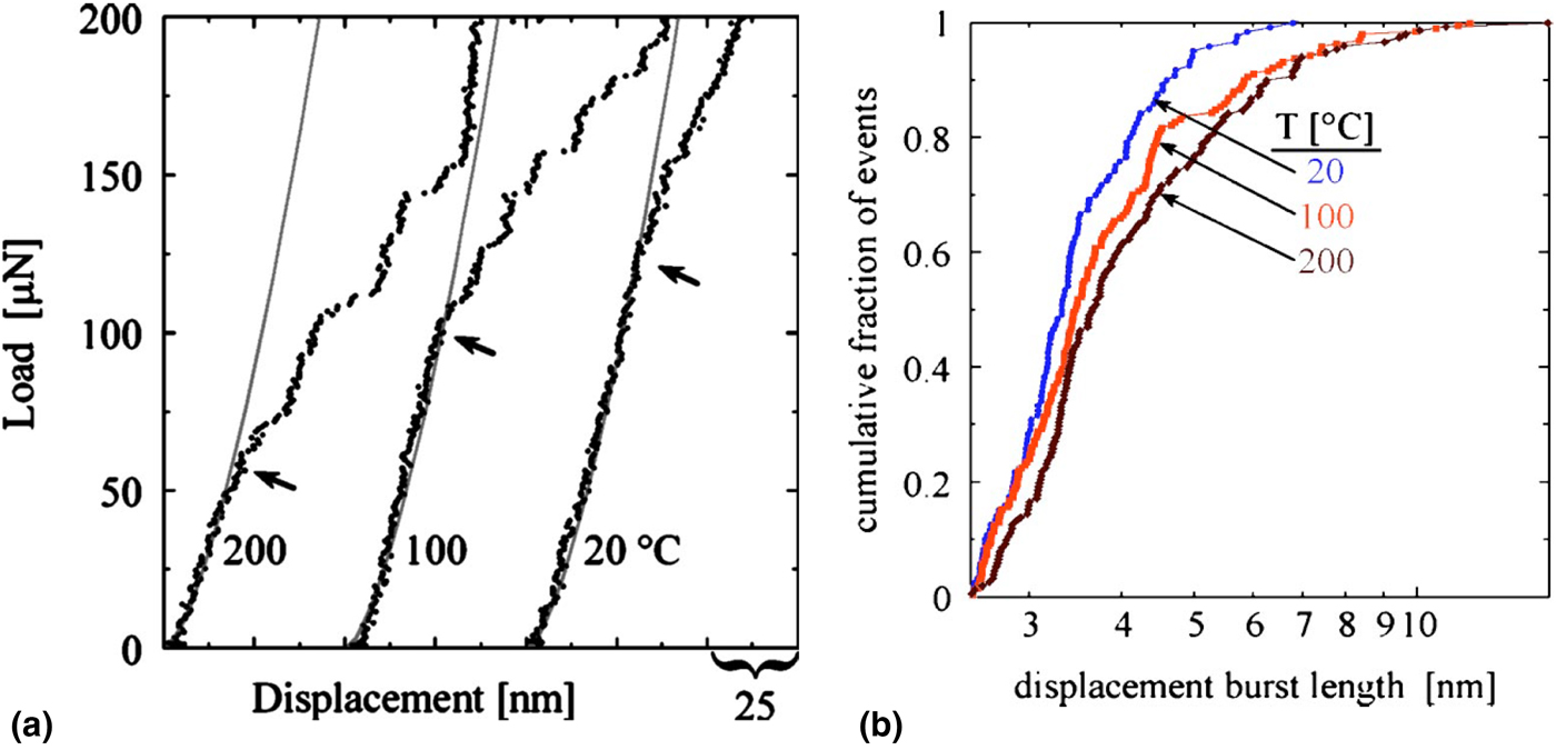
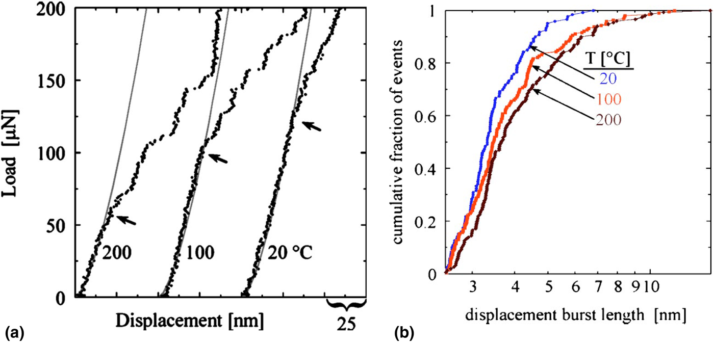
As seen in Figs. 4(a) and 4(b), indentation of pure Pt at high temperatures leads to the discretization of plasticity into sharp bursts of activity. Based on the complementary mathematical approaches,[ Reference Lund, Hodge and Schuh 28 , Reference Schuh, Mason and Lund 29 ] the onset of plasticity of Pt is explained by heterogeneous process of dislocation nucleation, with an atomic-scale, low-energy event as the rate limiter.[ Reference Mason, Lund and Schuh 30 ] An analysis based on the total activation energy and activation volume indicates that screw dislocation cross-slip governs the operative plastic deformation of Mg, regardless of the strain rate and temperature (<300 °C).[ Reference Haghshenas, Bhakhri, Oviasuyi and Klassen 31 ] Nanoindentation experiments of high-purity Cr have also revealed the existence of thermally-activated strength component superimposed on a temperature-/rate-independent strength contribution, attributable to the propagation of screw dislocations governed by thermally-activated kink-pair nucleation.[ Reference Choi, Brandl and Schwaiger 32 ] Similarly, indentation plastic deformation of ultrafine-grained (UFG) Cu-Nb composite with a randomly distributed oriented grain size ~100–200 nm up to 300 °C is controlled by dislocation glide and nucleation of kink pairs. However, the plasticity mechanism changes to thermally-activated processes at grain boundaries (GBs) at higher temperatures.[ Reference Primorac, Abad, Hosemann, Kreuzeder, Maier and Kiener 33 ] As for the UFG Al with a grain size of ~400 nm, when the temperature increases, the type of dislocation interaction with GBs changes from dislocation motion along GBs to dislocations emitted from GBs into the lattice and finally, at the highest temperatures, to diffusion of Al along the GBs. The onset of diffusion-based deformation is observed at lower temperatures for UFG Al than for conventional grained (CG) Al with grain size of ~80 µm, which is consistent with that the GB activity increases with decreasing grain size. Creep behavior during the indentation strain rate jumps, where several abrupt changes in the applied strain rate at defined indentation depths during one single indentation are used,[ Reference Maier, Durst, Mueller, Backes, Höppel and Göken 34 ] is thought to have masked any change in the activation volume at elevated temperatures.[ Reference Wheeler, Maier, Durst, Göken and Michler 35 ]
(a) P-h curves from the nanoindentation of Pt (100) at different temperatures, (b) cumulative fraction of pop-in events. Displacement bursts increase with temperature. Adopted with permission from Ref.[Reference Lund, Hodge and Schuh28] (American Institute of Physics, 2004).
Plasticity of non-crystalline materials
Bulk metallic glasses (BMGs) have recently attracted much interest, primarily due to their exclusive combination of mechanical and functional properties. One of the most momentous thermophysical properties of BMGs is the glass transition temperature (T g ), higher than which a transition from a hard and relatively brittle glassy state into a viscous or rubbery state occurs. If a BMG is heated to a considerable fraction of its T g , ~0.75 T g or higher, its strength decreases significantly as a result of delocalization of deformation as well as homogeneous occurrence of diffuse strain accommodation throughout the stressed material. High temperature nanoindentation studies in Au49Ag5.5Pd2.3Cu26.9Si16.3 BMG show that inhomogeneous-to-homogeneous flow transition and reverse ISE occurs when the temperature approaches T g = 130 °C,[ Reference Li, Liu, Chan, Chen and Pan 36 , Reference Yang, Wadsworth and Nieh 37 ] which can be explained in terms of the free volume theory.[ Reference Li, Liu, Chan, Chen and Pan 36 ] Notice that the free volume model[ Reference Argon 38 – Reference Zallen 40 ] can be adopted to calculate the volume of a basic shear flow unit STZ and the thermal activation energy of a metallic glass.
Amorphous Pd40Ni40P20 and Mg65Cu25Gd10 metallic glasses have demonstrated two different regimes of homogeneous flow under nanoindentation loading: the first one correlates with the onset of viscous deformation at high temperatures and low rates; the second one corresponds to the high rates at temperatures well below the glass transition, and arises when the deformation rate exceeds the characteristic rate for shear band nucleation, kinetically forcing strain distribution.[ Reference Schuh, Lund and Nieh 41 ]
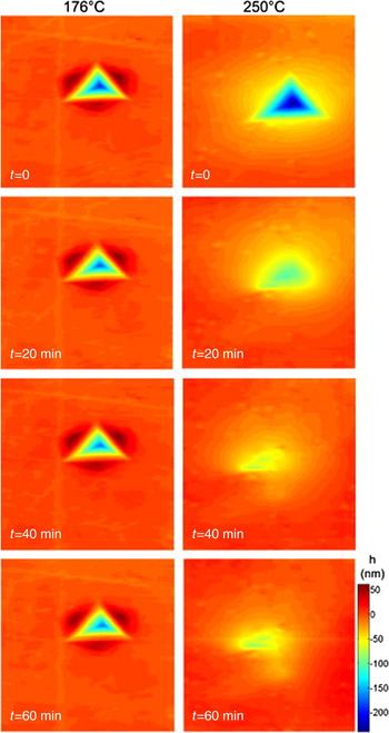
Figure 5 compares a time-series of topographical images of single indentations implemented at 176 and 250 °C on Pt57.5Cu14.7Ni5.3P22.5 metallic glass, where the viscous-plastic shape recovery at high temperatures is observed due to the surface-tension-driven viscous flow.[ Reference Packard, Schroers and Schuh 42 ] Such surface tension of metallic glasses in the supercooled liquid temperature range can be modeled by an elastic-viscoplastic constitutive theory developed by Henann and Anand.[ Reference Henann and Anand 43 ] Self-smoothing of metallic glass surfaces[ Reference Kumar and Schroers 44 ] is also witnessed at temperatures above T g.[ Reference Packard, Schroers and Schuh 42 ]
Topographic images of two indentations in Pt-based metallic glass at 176 and 250 °C after unloading, illustrating relative stability and substantial shape recovery, respectively. h in the legend indicates the surface roughness. Adopted with permission from Ref.[Reference Packard, Schroers and Schuh42] (Elsevier, 2009).

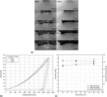
As seen in Fig. 6(a), for similar levels of penetration depth, the high-temperature indentations in Zr-based BMG demonstrate considerably fewer numbers of shear offset displacements than at room temperatures. Also, the onset of shear offsets transpires at higher depths of penetration, culminating in a lower total pile-up at the edge of the indentation. Temperature also affects the morphology of the shear offsets, i.e., at room temperature a pointed apex is seen while at 200 °C, a smooth semi-circular aspect is realized. P-h curves presented in Fig. 6(b) indicate the increase of serrated flow with temperature.[ Reference Wheeler, Raghavan and Michler 45 , Reference Bhattacharyya, Singh, Prasad, Narasimhan and Ramamurty 46 ] Fig. 6(c) demonstrates that hardness of Zr-based BMG increases linearly with temperature from an average of 7 GPa at 25 °C to 7.6 GPa at 200 °C, while the reduced Young's modulus marginally decreases from 105 GPa to 103 GPa. The increase of hardness with temperature is explained by the increase of friction and energy consumed by the progressively thermally favored formation/reactivation of shear band deformation, which is prevented from contributing to a total penetration depth in the form of pop-ins during the displacement-controlled indentation.[ Reference Wheeler, Raghavan and Michler 45 ]
(a) In-situ scanning electron microscopy (SEM) pile-up deformation of a Zr-based BMG at 25 °C and 200 °C, (b) P-h curves for indentations loaded at 1 mN/s at different temperatures, (c) Hardness and reduced modulus as a function of temperature. Adopted with permission from Ref.[Reference Wheeler, Raghavan and Michler45] (Elsevier, 2011).

Phase transformation
Indentation with a nanoscale tip is known to induce a phase transformation in Si at room temperature. Minomura and Drickamer[ Reference Minomura and Drickamer 47 ] were the first to discover the change of conductivity of Si under high-pressure loading, explained by a semiconductor–metal phase transition. Under room temperature condition, Si transforms to a metallic phase with β-Sn (Si-II) structure at a pressure of ~11–13 GPa, and further phase transforms (depending on unloading conditions) to amorphous silicon (a-Si) and/or the high-pressure crystalline phases Si-III (bc8, body-centered cubic (BCC) structure), and Si-XII (r8, the rhombohedral distortion of bc8) on unloading, which shows semi-metallic electronic behaviors.[ Reference Ge, Domnich and Gogotsi 48 – Reference Chavoshi, Gallo, Dong and Luo 51 ] In-situ high-temperature nanoindentation studies uncover that the Si-II phase is unstable in a pristine Si matrix at high temperatures. The nucleation of Si-III and Si-XII phases during unloading is intensified with the increase of temperature, however, the final phases depend on their thermal stability.
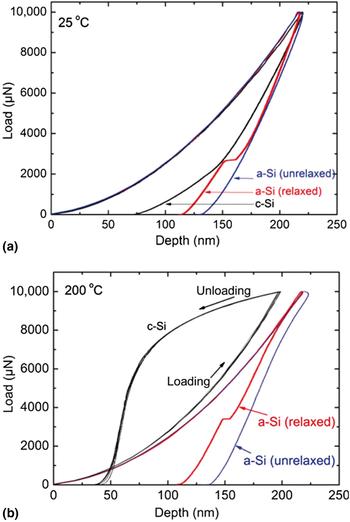
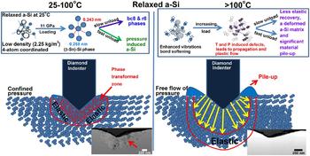
As shown in Fig. 7, an unusual “bowing” occurs on the P-h curve at 200 °C, which is attributed to the direct Si-II to Si-I transformation accompanied by rapid volume expansion. In fact, “bowing” phenomenon is detected for temperatures above ~125 °C. Furthermore, due to the rapid volume expansion as a result of the abrupt formation of Si-III/Si-XII during unloading of relaxed a-Si (relaxed by annealing), a pop-out event happens. However, no pop-out occurs for the unrelaxed a-Si.[ Reference Bhuyan, Bradby, Ruffell, Haberl, Saint, Williams and Munroe 52 , Reference Ruffell, Bradby, Williams, Munoz-Paniagua, Tadayyon, Coatsworth and Norton 53 ] Kiran et al.[ Reference Kiran, Haberl, Williams and Bradby 54 ] showed that relaxed a-Si undergoes a pressure-induced phase transformation, either crystalline (Si-III/Si-XII) end phases or pressure-induced a-Si, at temperatures below 100 °C, as illustrated in Fig. 8.
P-h curves of pristine Si (c-Si), relaxed and unrelaxed a-Si at (a) 25 °C and (b) 200 °C. Unusual “bowing” behavior of pristine Si at 200 °C is observable. Relaxed a-Si shows a “pop-out” event. Adopted with permission from Ref.[Reference Bhuyan, Bradby, Ruffell, Haberl, Saint, Williams and Munroe52] (Cambridge University Press, 2012).

Deformation of relaxed a-Si at different temperatures. Adopted with permission from Ref.[Reference Kiran, Haberl, Williams and Bradby54] (American Institute of Physics, 2014).

However, at higher temperatures, plastic flow dominates the mode of deformation. It can be postulated that synergy of pressure and temperature can cause bond softening and defect formation in relaxed a-Si, resulting in the inhibition of phase transformation owing to pressure-releasing plastic flow beneath the indenter. Interestingly, unrelaxed a-Si does not undergo phase transformation; rather it deforms completely via plastic flow up to 200 °C.[ Reference Kiran, Haberl, Williams and Bradby 54 ] Si-VIII phase has also been observed during unloading at 100–125 °C,[ Reference Singh, Munroe and Hoffman 55 ] whereas at temperatures above 350 °C, no phase transformation has been reported.[ Reference Domnich, Aratyn, Kriven and Gogotsi 56 ]
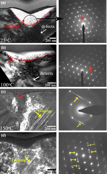
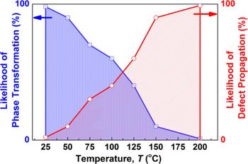
Figure 9 presents the cross-sectional TEM (XTEM) bright and dark-field images of residual Berkovich indents of Si at different temperatures, along with selected area diffraction (SAD) patterns from the regions directly underneath the residual indents. Indents made at 25 and 100 °C, Figs. 9(a) and 9(b), show the presence of phase transformed zones within the deformed volume. Apart from Si reflections, there are several extra diffraction spots which are known to be characteristic reflections from polycrystalline Si-III and/or Si-XII phases. At 150 and 200 °C, only a very small phase transformed volume can be noticed. However, twinning along {111} planes is dominant at these temperatures, as illustrated in Figs. 9(c) and 9(d). Figure 10 depicts the deformation processes in Si under a nanoscale Berkovich indenter in the temperature range 25–200 °C, signifying that both phase transformation and defect propagation occur but to different extents depending on the indentation temperature.[ Reference Kiran, Tran, Smillie, Haberl, Subianto, Williams and Bradby 57 ]
(a) and (b) Bright-field and (c) and (d) Dark-field XTEM images along with the SAD patterns of Berkovich indents indented on Si. Diffraction spots from bc8/r8 are pointed to by red arrows. The yellow arrows in (c) and (d) represent twinning and in their corresponding SAD patterns represent streaking and spot splitting due to twinning, respectively. For clarity, the red lines in (a), (b), and (c) illustrate the boundary between phase transformed and untransformed volumes under the indenter. Adopted with permission from Ref.[Reference Kiran, Tran, Smillie, Haberl, Subianto, Williams and Bradby57] (American Institute of Physics, 2015).

Schematic of the temperature dependence of the deformation mechanisms of diamond cubic Si under a nanoscale Berkovich indenter. Adopted with permission from Ref.[Reference Kiran, Tran, Smillie, Haberl, Subianto, Williams and Bradby57] (American Institute of Physics, 2015).

It is worthwhile to note that due to its technological importance, Si has remained an interesting material for high-temperature deformation mechanism studies and it is expected that, by using novel in-situ observation techniques, further issues will be uncovered in the following years. On the other hand, although Si and Ge are well-characterized materials in semiconductor section, other semiconductors, such as lithium niobate (LiNbO3 or LN), have not been explored as systematically. LN is also called the “silicon of photonics”, and is indispensable in advanced photonics and nonlinear optics. Furthermore, since these semiconductors should be cut and polished to produce a qualified wafer, they undergo several mechanical treatments which are directly associated with their deformation behavior at higher temperatures. These issues certainly point to the need for further research specifically addressing the role of temperature on the fundamental mechanical deformation of such semiconductor materials.
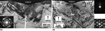
TEM images in Fig. 11 demonstrate that at room temperature, the transformed region in Ge comprises a BCC structure and the original diamond structure, whereas at 400 °C twinning in the diamond structure mainly drives the deformation. SAD analysis also reveals the presence of hexagonal structure at high temperatures,[ Reference Vandeperre, Giuliani, Lloyd and Clegg 58 ] both at the intersection of twins and in ribbons by the passage of a secondary twin,[ Reference Xiao and Pirouz 59 ] indicating that the pressure-induced phase transformation to the β-Sn structure occurs at 400 °C. This observation is in line with the fact that hardness (4 ± 1 GPa) is lower than the pressure required to induce the phase transformation (~7–10 GPa, depending on the presence of shear stresses.[ Reference Menoni, Hu and Spain 60 ])
TEM bright-field image demonstrating (a) Phase transformation in Ge, marked ‘t’, at room temperature, (b) Hexagonal crystal structure (‘cr’) and twinning (‘tw’) at 400 °C. Adopted with permission from Ref.[Reference Vandeperre, Giuliani, Lloyd and Clegg58] (Elsevier, 2007).

Analysis of the high-temperature nanoindentation of shape memory alloy (SMA) Ni-Ti at 110 °C confirms that the martensite phase is converted to austenite at high temperatures, which demonstrates the mechanical properties akin to the austenite at room temperature, underscoring the thermally-induced phase transformations of Ni-Ti. Besides, the Young's modulus and hardness of the martensite films are smaller than those of the austenite films.[ Reference Huang, Nohava, Zhang and Ramirez 61 ] Pseudoelasticity (also referred to as superelasticity) of SMAs is usually linked with the reversible austenite-martensite phase transformation characterized by diffusionless, shear-induced atomic rearrangement. The occurrence of pseudoelasticity of martensitic Ni-Ti films is possible at the nanoscale over a specific temperature range without the evolution of martensite-austenite transformation. At an intermediate temperature of 55 °C, the anomalous pseudoelastic behavior of martensitic Ni-Ti films driven by increased twinned structure mobility can be realized.[ Reference Ma and Komvopoulos 62 ] The deformation mechanisms and the energy dissipated in the martensitic Ni-Ti films which exhibit pseudoelasticity are usually interpreted in terms of the behavior of metastable pseudotwins in the stress-induced martensite.[ Reference Ma and Komvopoulos 62 , Reference Komvopoulos and Ma 63 ]
Mechanical properties
High-temperature nanoindentation can be used for measuring mechanical properties of materials, mainly hardness and elastic modulus, at elevated temperatures. For high-temperature nanoindentation and/or viscoelastic-plastic materials, e.g., polymeric materials, where the deformation is time-dependent and pile-up or sink-in is significant around the contact impression, the modified Oliver-Pharr method has to be adopted, where the true (elastic) contact stiffness, S e , is used:[ Reference Li, Fang, Lu, Yu, Hou and Feng 64 , Reference Feng and Ngan 65 ]
 $$\displaystyle{1 \over {S_e}} = \displaystyle{1 \over S} + \displaystyle{{{\dot h}_h^\alpha} \over {\left \vert {\dot P} \right \vert}} $$
 $$E_r = \displaystyle{{\sqrt \pi} \over {2\beta}} \displaystyle{{S_e} \over {\sqrt A}} $$
 $$\displaystyle{1 \over {E_r}} = \displaystyle{{1 - v^2} \over E} + \displaystyle{{1 - v_i^2} \over {E_i}}$$
 $$H = \displaystyle{P \over A}$$
where
 $\dot h_h$
is the indenter displacement rate at the onset of unloading,
 $\left \vert {\dot P} \right \vert$
is the unloading rate, α is a positive dimensionless constant exponent, β is the correction factor for the indenter shape (β = 1.034–1.09 for a Berkovich indenter), E
r
is the reduced modulus, A is the contact area, E, ν and E
i
, ν
i
stand for the elastic Young's modulus and Poisson's ratio of the sample and indenter, respectively. The hardness of the sample is calculated from Eq. 4.
Another recently-developed technique is to calculate a correction factor for the contact area calculated using the surface acoustic wave (SAW)[ Reference Rogers, Maznev, Banet and Nelson 66 ] measurement which allows a correct hardness value, accounting for the pileup, to be determined.[ Reference Beck, Hofmann, Eliason, Maznev, Nelson and Armstrong 67 ] This is a new and interesting approach for determining the true hardness and modulus which is expected to be pursued further in the coming years. An alternative method is the direct imaging of the residual impression[ Reference Fujisawa and Swain 68 ] to determine the projected area. Such direct imaging technique is suitable for the cases where the edges of the residual indent impression (phase transformed or plastically deformed zone) are clearly visible owing to changes in surface morphology. In other words, the measurement of the indentation hardness by direct imaging is only correct if the measurement of the projected area captures the full phase transformed or plastically deformed area during loading.[ Reference Haberl, Aji, Williams and Bradby 69 ]
Notice open questions regarding the oxide film/substrate system still remain, particularly for high-temperature nanoindentation experiments. Although a preparatory explanation for the effect of the oxide film on the mechanical properties of a substrate was proposed by Tsui and Pharr,[ Reference Tsui and Pharr 70 ] further experimental and theoretical work are required to pinpoint the impact of oxide film/substrate system on the measured modulus and to propose new schemes to eliminate it from the measurements.
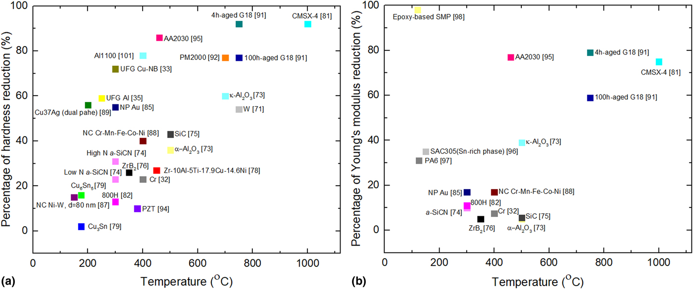
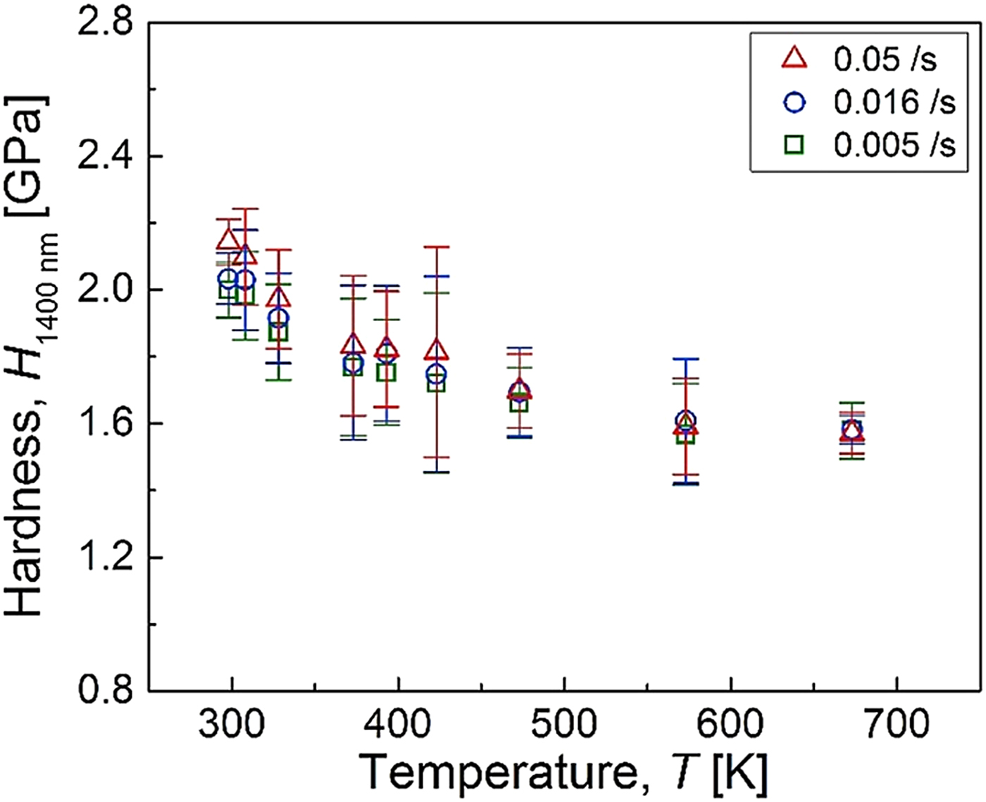
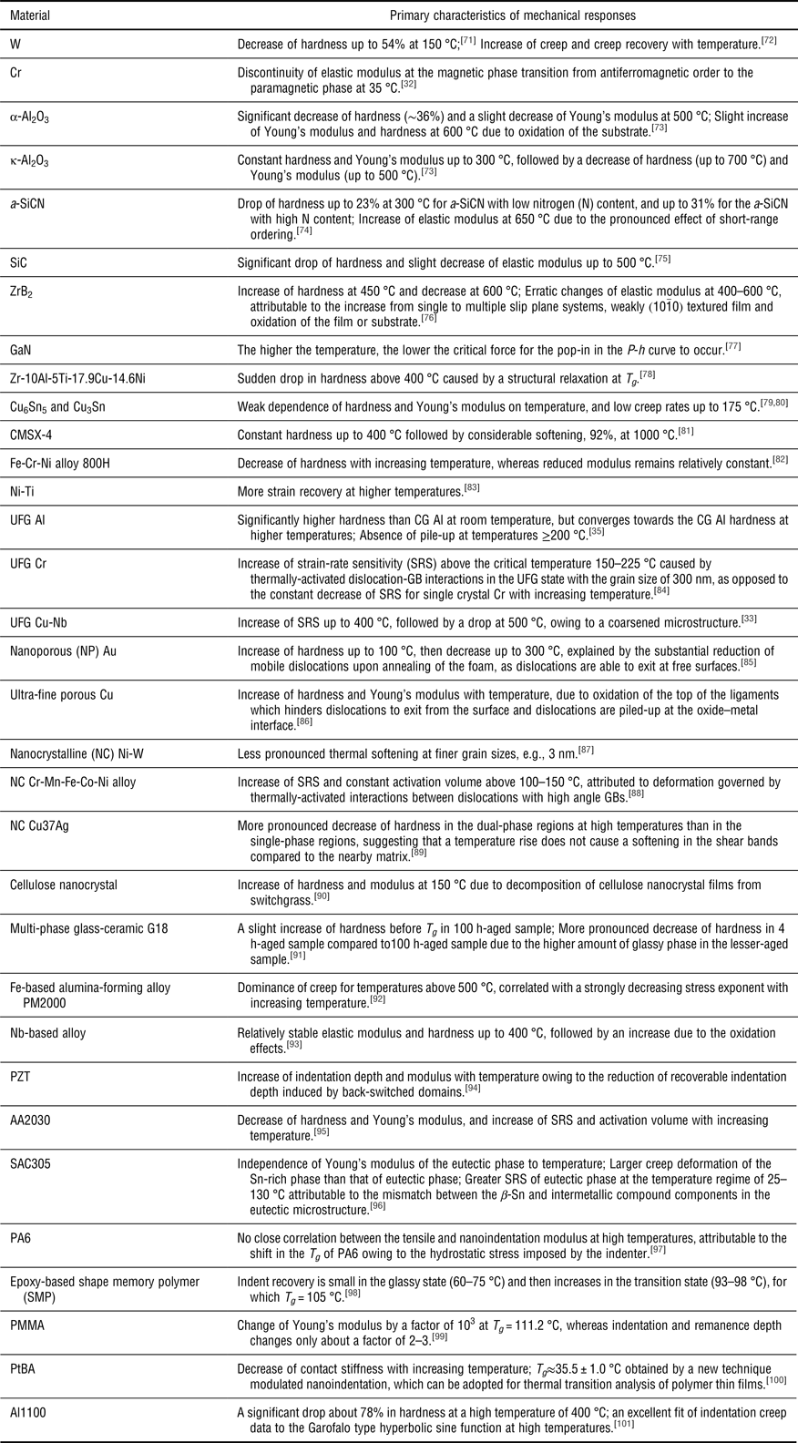
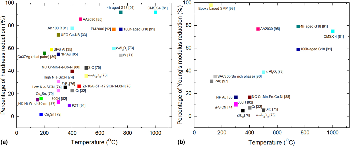
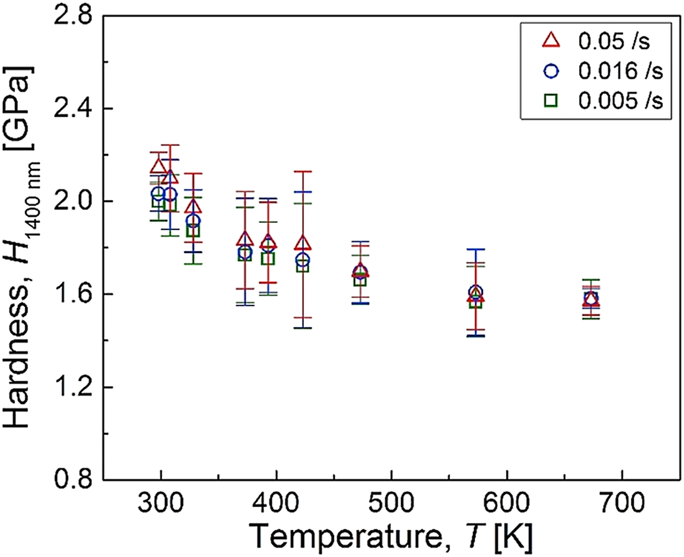
While the detailed literature on the determination of mechanical properties using high-temperature nanoindentation is extensive, most work identically reported the deterioration of mechanical properties with increasing temperature. Figure 12 illustrates the temperature versus percentage of hardness/Young's modulus reduction with respect to the room temperature values for different materials. Clearly, hardness is more affected by the temperature than Young's modulus. In support to Fig. 12, some interesting findings on the indentation response of materials at high temperatures are summarized in Table 1. It is instructive to note that the effect of nanoindentation speed (loading rate) on the resulting mechanical properties of materials is less pronounced at high temperatures. For example, as seen in Fig. 13, indentation hardness of high-purity Cr becomes strain-rate independent at a high temperature of 400 °C.[ Reference Choi, Brandl and Schwaiger 32 ] Less pronounced ISE at high temperatures has also been observed for Fe-Cr-Ni alloy 800H, which is attributed to the larger plastic zone size or the storage volume of geometrically necessary dislocations (GNDs).[ Reference Prasitthipayong, Vachhani, Tumey, Minor and Hosemann 82 ]
Percentage of (a) hardness (b) Young's modulus reduction as a function of temperature. The percentage values are calculated with respect to their values at room temperature. For further information, see Table 1.
Indentation hardness of high-purity Cr as a function of temperature and strain-rate. Adopted with permission from Ref.[Reference Choi, Brandl and Schwaiger32] (Elsevier, 2017).
Overview of nanoindentation mechanical responses of different materials at high temperatures.

As a final note, we remark that the location where the indenter is applied, e.g., GB or grain interior, can affect the nanoindentation response of the nano/polycrystalline materials. The same goes for the multi-phase materials, where various grains belonging to the same phase could have different grain size, elemental distribution, and grain orientation. For instance, room temperature indentation studies of a multi-phase quench and partitioning (Q&P) steel indicate that indentation hardness generally decreases with increasing distance from the GB in tempered martensite, which is attributed to the higher GNDs density near the GB, GB strengthening or carbon diffusion from martensite to retained austenite during the partitioning process.[ Reference Cheng, Choi, Hu and Sun 102 ] On the other hand, the grains of the ferrite phase in a dual phase steel are found to be harder in the vicinity of martensitic grains.[ Reference Kadkhodapour, Schmauder, Raabe, Ziaei-Rad, Weber and Calcagnotto 103 ] Higher values of indentation hardness of austenitic phase compared to ferritic in transformation-induced plasticity steels, and specific pop-in events resulting from the onset of strain-induced martensitic transformation has also been reported,[ Reference Ahn, Oh, Kim, Oh, Bei, George and Han 104 , Reference He, Huang, Liang, Ngan, Luo, Shi, Cao and Dong 105 ] which contradicts the hardness values obtained from the austenitic-ferritic duplex stainless steel, where the ferrite is the harder phase.[ Reference Gadelrab, Li, Chiesa and Souier 106 ] These room temperature studies point to the fact that one should be careful while measuring nanomechanical properties of multi-phase materials using nanoindentation instrument at low and high temperatures. It may also be noted that in spite of relatively detailed knowledge about the room temperature nanoindentation of multiphase steels, the temperature-dependent indentation behavior and high-temperature phase transformation of martensite, austenite, and ferrite in multiphase steels remains unexplored. This is an exciting area of further research which is encouraged for future work.
Remarks and perspective
Engineering materials exhibit temperature dependency in their physical and mechanical properties, arising from activities of phonons (crystalline insulators and some semi-conductors), electrons (metal and some semi-conductors), propagons, diffusons, and locons (amorphous non-metallic materials), as well as thermal activation and phase transformation processes. A fundamental understanding of the temperature effects on the nanomechanical behavior and corresponding underlying mechanisms of nanostructured materials in the temperature regime of interest is critical for designing and developing micro/nanoelectromechanical systems, where surface atoms in contact regions are subjected to certain forms of loading at service temperatures. High-temperature nanoindentation renders a novel approach to uncover the nanomechanical behavior at elevated temperatures as well as thermally-activated processes and incipient plasticity in materials. In particular, recent breakthrough in in-situ high-temperature nanoindentation measurements, e.g., in-situ SEM,[ Reference Wheeler and Michler 7 , Reference Wheeler, Raghavan and Michler 45 , Reference Wheeler, Niederberger, Tessarek, Christiansen and Michler 107 ] in-situ Raman, in-situ TEM techniques, allow the real-time study of the interplay between mechanical, thermal, and electrical effects at the nanoscale. In general, the ability to implement multiple measurements simultaneously and to combine information from multiple analyses and techniques is highly desirable for nanoscale material characterization at high temperatures. As a result of the great capability of the in-situ measurements, it is envisioned that this arena will be pursued further by researchers in the upcoming years. Such technical advances in in-situ high-temperature nanoindentation instrumentation and their capabilities can benefit other in-situ thermomechanical testing methods such as high-temperature microcompression, as identical equipment can be used for characterization of multi-functionality at the nanoscale.
In addition, knowledge of the true contact area is very important for the successful determination of indentation hardness and modulus. One paramount consideration when determining the mechanical properties of materials is that, although conventional methods such as the Oliver-Pharr[ Reference Oliver and Pharr 108 ] and Field-Swain[ Reference Field and Swain 109 ] approximations for estimating contact depth are robust and directly applicable to room temperature nanoindentation and elastic-plastic materials, measurements of the contact depth for high temperature nanoindentation and/or viscoelastic-plastic materials, where deformation is time-dependent and pile-up or sink-in is significant around the contact impression, ought to be conducted using modified schemes such as the modified Oliver-Pharr method[ Reference Feng and Ngan 65 ] to avoid any over-estimation of the reduced modulus and hardness. New methods and measurement techniques such as SAW[ Reference Beck, Hofmann, Eliason, Maznev, Nelson and Armstrong 67 ] and direct imaging of the residual impression[ Reference Fujisawa and Swain 68 ] can also be adopted to tackle this challenging problem. Such issues remain unsolved for most commercial nanoindentation instruments. It is therefore anticipated that determination of the true hardness and modulus will be advanced further in the near future.
Finally, we remark that with further advancements in computational modeling techniques, it will be feasible to gain clear insights into the temperature-dependent nanoindentation behavior and thermally-activated processes in functional materials. Particularly, a combination of the atomistic-based modeling and in-situ nanoindentation experiments provides a promising means to address the defect formation processes in crystalline and non-crystalline materials.
Acknowledgment
SZC would like to express his sincere gratitude for the financial support from the BIAM-Imperial Centre for Materials Characterization, Processing, and Modeling at Imperial College London. The work of SX was supported in part by the Elings Prize Fellowship in Science offered by the California NanoSystems Institute (CNSI) on the UC Santa Barbara campus.