I. INTRODUCTION
The carbon–nitrogen (C–N) compounds have long been attracting interest due to their versatile and unique properties. It is known that diamond is the hardest material in nature with measured Vickers hardness up to 120 GPa. Reference Brazhkin, Dubrovinskaia, Nicol, Novikov, Riedel, Solozhenko and Zhao1 Liu and Cohen Reference Liu and Cohen2 creatively predicted that β-C3N4 with the ultrahigh bulk modulus of ∼430 GPa is a superhard material even harder than diamond, which highlights the pivotal role of strongly covalent C–N bonds. Although β-C3N4 as a hypothetical material has not yet be synthesized, it stimulates intensive studies on the carbon nitrides with manifold stoichiometries, including sp 3-hybridized dense phases (CN, Reference Zhang, Wei, Yan, Zhao and Wang3,Reference Hart, Claeyssens, Allan and May4 C3N2, Reference Tian, Wang, He, Ma, Wang, Cui, Chen, Liu and Zou5 C3N, Reference Hart, Claeyssens, Allan and May4,Reference Hao, Liu, Lei, Tang, Lu, Liu and Li6 etc.) and sp 2-hybridized graphitic phases (CN, Reference Hart, Claeyssens, Allan and May4 C3N, Reference Hart, Claeyssens, Allan and May4,Reference Hao, Liu, Lei, Tang, Lu, Liu and Li6–Reference Hu, Wu, Wang, He and Zhang8 etc.), which are typically useful for superhard materials Reference Dong, Oganov, Zhu and Qian9 and (photo) catalyst, Reference Goettmann, Fischer, Antonietti and Thomas10,Reference Wang, Maeda, Thomas, Takanabe, Xin, Carlsson, Domen and Antonietti11 respectively.
In two-dimensional (2D) scenario, graphene, a single-layer of carbon atoms arranged in a honeycomb lattice, possesses superior physical and chemical properties and carries great promise for various device applications. Reference Pati, Enoki and Rao12 In particular, graphene is the strongest 2D material which exhibits ultra-high Young’s modulus and unsurpassed tensile strength. Reference Lee, Wei, Kysar and Hone13 Doping graphene with nitrogen atoms is widely considered an effective way to further tailor its electronic structure as well as other physical and chemical properties. Reference Deng, Pan, Yu, Cui, Jiang, Qi, Li, Fu, Ma, Xue, Sun and Bao14,Reference Zhao, He, Rim, Schiros, Kim, Zhou, Gutiérrez, Chockalingam, Arguello, Pálová, Nordlund, Hybertsen, Reichman, Heinz, Kim, Pinczuk, Flynn and Pasupathy15 Monolayer C3N, a kind of 2D nitrogen-graphene crystal, was first reported to be an indirect band-gap semiconductor by Mizuno et al. Reference Mizuno, Fujita and Nakao16 using early-stage electronic structure method. Recently, Hu et al. Reference Hu, Wu, Wang, He and Zhang8 suggested three possible planar structures of C3N and the most stable one in energy is the same as that proposed in Ref. Reference Mizuno, Fujita and Nakao16. By using the cluster-expansion and particle-swarm optimization algorithms, Xiang et al. Reference Xiang, Huang, Li, Wei, Yang and Gong17 studied in detail the C–N phase separation in nitrogen-doped graphene and two stable, ordered, and semiconducting nitrogen-graphene crystals, C3N and C12N, are revealed. Up to date, only monolayer C3N is synthesized in experiment via the direct pyrolysis of hexaaminobenzene trihydrochloride single crystals in the solid state. Reference Mahmood, Lee, Jung, Shin, Choi, Seo, Jung, Kim, Li, Lah, Park, Shin, Oh and Baek18 Very recently, Yang et al. Reference Yang, Li, Ye, Wang, Tian, Zhu, He, Ding, Xie, Liu, Lifshitz, Lee, Kang and Jiang19 fabricated large-scale C3N nanostructures from the polymerization of 2,3-diaminophenazine by a hydrothermal treatment, and further exhibited a ferromagnetic order at low temperatures when hydrogen atoms are doped. Although the electronic structure of monolayer C3N has been described several times in previous literature, Reference Hu, Wu, Wang, He and Zhang8,Reference Mizuno, Fujita and Nakao16–Reference Mahmood, Lee, Jung, Shin, Choi, Seo, Jung, Kim, Li, Lah, Park, Shin, Oh and Baek18 more detailed studies on its other physical properties, such as the optical and mechanical performances, are still lacking so far. Therefore, it is urgent to understand deeply this 2D C–N material thoroughly so as to bring about possible engineering applications in the future.
In this work, based on the first-principles density functional theory, we investigate the electronic, mechanical, and optical properties of monolayer C3N. We find that monolayer C3N is an indirect band-gap semiconductor with the gap of 1.042 eV and this value determined by accurate hybrid functional is much larger than previous results calculated by conventional exchange-correlation functionals (0.2–0.3 eV). Reference Hu, Wu, Wang, He and Zhang8,Reference Xiang, Huang, Li, Wei, Yang and Gong17,Reference Mahmood, Lee, Jung, Shin, Choi, Seo, Jung, Kim, Li, Lah, Park, Shin, Oh and Baek18 Monolayer C3N is weaker than graphene under ultimate tensile strains due to its smaller ideal strength, while interestingly, monolayer C3N presents larger in-plane stiffness than graphene. The nonlinear effect of elasticity is explored and it is more prominent in monolayer C3N rather than graphene. Moreover, we calculate the optical properties of monolayer C3N and find that the main and secondary absorption peaks are respectively located in visible and ultraviolet light regions and their ratio can be effectively mediated by strain.
II. COMPUTATIONAL DETAILS
Our first-principles calculations are performed based on the density functional theory as implemented in the Vienna ab initio simulation package (VASP). Reference Kresse and Furthmüller20,Reference Kresse and Furthmüller21 The interaction between ionic cores and valence electrons is described by the projected augmented wave method. Reference Blöchl22 The valence configurations of C and N atoms are 2s 22p 2 and 2s 22p 3 respectively. The exchange-correlation effect is treated with the Perdew, Burke, and Ernzerhof parameterized generalized-gradient approximation (PBE-GGA). Reference Perdew, Burke and Ernzerhof23 To obtain more accurate band structures and optical properties, the hybrid functional (HSE06) Reference Heyd, Scuseria and Ernzerhof24 is further used. For the slab model, a vacuum space with the thickness of 11 Å is used to avoid the interactions between adjacent monolayers. The energy cutoff of plane wave is 550 eV and the Monkhorst–Pack k-mesh Reference Monkhorst and Pack25 of 9 × 9 × 1 and 11 × 11 × 1 are used for lattice relaxations and static self-consistent field calculations respectively. The conjugate gradient algorithm is used to optimize the atomic positions until the forces on each atom are less than 0.005 eV/Å and the electronic ground states are convergent within an energy criterion of 10−6 eV. The strain is defined as ε = (l − l 0)/l 0 × 100%, where l and l 0 are strained and balanced lattice constants. For uniaxial strains, the transverse lattice beyond the strained direction together with the atomic positions is well relaxed. The stress and dielectric functions are scaled by a factor of z/d 0 to exclude the vacuum region, where z is the cell length normal to the atomic plane and d 0 = 3.7 Å the effective thickness of monolayer C3N estimated from its bulk form. Reference King, Matthews, Holgado, Jefferson, Lambert, Alavi and Wright26 The phonon spectrum is performed by the density functional perturbation theory (DFPT), which can accurately capture the phonon instability and ideal strength. Reference Baroni, de Gironcoli, Dal Corso and Giannozzi27,Reference Liu, Ming and Li28 The optical properties are calculated according to the Kubo–Greenwood formula within the linear response theory, Reference Kubo29,Reference Wang and Callaway30 implemented in the WANNIER90 package. Reference Mostofi, Yates, Lee, Souza, Vanderbilt and Marzari31
III. RESULTS AND DISCUSSION
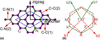
Structurally, monolayer C3N possesses a planar honeycomb lattice, shown in Fig. 1(a), which consists of six C atoms and two N atoms. It can be regarded as a 2 × 2 graphene supercell substituted by two N atoms, which cut carbon network to separated benzene rings. The optimized lattice constant of monolayer C3N is 4.862 Å, which agrees well with the experimental value of 4.75 Å. Reference Mahmood, Lee, Jung, Shin, Choi, Seo, Jung, Kim, Li, Lah, Park, Shin, Oh and Baek18 The C–C and C–N bond lengths are almost equivalent at strain-free case, i.e., 1.404 and 1.403 Å respectively, which are in good accordance with previous theoretical calculation. Reference Xiang, Huang, Li, Wei, Yang and Gong17 The atomic bond lengths of C3N are slightly smaller than that of graphene (1.42 Å). Under uniaxial strains along armchair or zigzag directions, both C–C and C–N bonds will develop to two nonequivalent ones [see Fig. 1(a)].
(a) Crystal structure of monolayer C3N. Blue dashed lines indicate the primitive cell which contains six C atoms and two N atoms. (b) Brillouin zones of monolayer C3N without strain (green solid lines) and under uniaxial strains (red dashed lines).

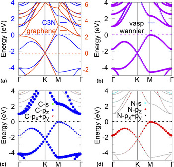
The band structures of monolayer C3N are shown in Fig. 2. One can see from Fig. 2(a) that graphene is a semimetal with a Dirac cone located at the K point while C3N is a semiconductor with the indirect band gap of 1.042 eV (HSE calculation). This is because the lowest conduction band of graphene is fully occupied by two electrons of substituted N atoms, such that the Dirac point in monolayer C3N is lowered by 2.25 eV below the Fermi energy. From the orbital-projected band structure shown in Figs. 2(c) and 2(d), one can further confirm that the highest valence band of monolayer C3N is dominated by p z orbitals of N atoms and the Dirac cone is still formed by p z orbitals of C atoms. The band gap of monolayer C3N has been measured by two recent experimental works. Reference Mahmood, Lee, Jung, Shin, Choi, Seo, Jung, Kim, Li, Lah, Park, Shin, Oh and Baek18,Reference Yang, Li, Ye, Wang, Tian, Zhu, He, Ding, Xie, Liu, Lifshitz, Lee, Kang and Jiang19 In the former work, Reference Mahmood, Lee, Jung, Shin, Choi, Seo, Jung, Kim, Li, Lah, Park, Shin, Oh and Baek18 the band gap is determined to be 2.67 eV by electrochemical method (i.e., the HOMO–LUMO gap). In the latter work, Reference Yang, Li, Ye, Wang, Tian, Zhu, He, Ding, Xie, Liu, Lifshitz, Lee, Kang and Jiang19 the band gap is determined to be 0.39 eV by the experimental measurement (UPS data and UV–vis data), and is confirmed by the first-principles calculation (on the GGA level). In our paper, the calculated band gap of monolayer C3N is 0.392 eV and 1.042 eV by the GGA and HSE potentials, respectively. Therefore, our GGA band gap is identical to the value in Ref. Reference Yang, Li, Ye, Wang, Tian, Zhu, He, Ding, Xie, Liu, Lifshitz, Lee, Kang and Jiang19, while our HSE band gap is in the middle of experimental results. Reference Mahmood, Lee, Jung, Shin, Choi, Seo, Jung, Kim, Li, Lah, Park, Shin, Oh and Baek18,Reference Yang, Li, Ye, Wang, Tian, Zhu, He, Ding, Xie, Liu, Lifshitz, Lee, Kang and Jiang19
(a) Band structures of monolayer C3N and 2 × 2 graphene. (b) Band structures of monolayer C3N by the first-principles calculation and the Wannier interpolation. (c, d) Band structures of monolayer C3N with orbital projections of C and N atoms. The Fermi energy is set to zero.

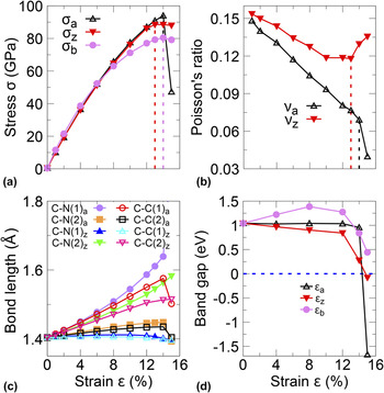
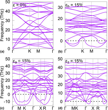
After briefly introducing the crystal and electronic structures of monolayer C3N, we give a detailed analysis on its mechanical properties with adequate comparisons to graphene. We first determine the ideal strength, the highest achievable mechanical strength of a defect-free crystal at zero temperature, Reference Roundy and Cohen32,Reference Luo, Roundy, Cohen and Morris33 by calculating the stress–strain curve which is presented in Fig. 3(a). The critical tensile strains before the material failure are 14%, 13%, and 14% in armchair, zigzag, and biaxial directions respectively, and the corresponding ideal strengths are 93.98, 88.52, and 80.46 GPa, indicating that monolayer C3N is weaker than graphene (110–121 GPa Reference Liu, Ming and Li28 and 125.37 GPa Reference Lee, Wei, Kysar and Hone13 ) due to relatively weaker C–N bonds. Since the peak stress at the critical strain is usually accompanied by phonon instability, we examine the phonon spectra on the strain paths using the DFPT method. Figure 4 shows that monolayer C3N at strain-free case is dynamically stable with positive phonon frequencies at all frequencies at all momenta, while different amounts of phonon softening indeed appear around the critical tensile strains (∼15%).
(a) Stress–strain curves of monolayer C3N. (b) Poisson’s ratios as a function of uniaxial strains. (c) Atomic bond length as a function of uniaxial strains. (d) Band gap as a function of biaxial and uniaxial strains. The subscripts a, z, and b mean the armchair, zigzag, and biaxial directions, respectively.

(a) Phonon spectrum of monolayer C3N without strain. (b)–(d) Phonon spectra of monolayer C3N at 15% tensile strains along biaxial (εb), armchair (εa), and zigzag (ε z ) directions. All phonon frequencies are positive below 15% tensile strains.

For uniaxial strain, the Poisson’s ratio ν = −εt/ε is carefully evaluated, where ε is the axial strain and εt is the transverse shrinkage perpendicular to the loading axis. Figure 3(b) shows the Poisson’s ratio as a function of uniaxial strain. For both armchair (a) and zigzag (z) directions, a value of νa(z)(ε = 0) ≈ 0.155 is obtained by extrapolating the stress–strain curve to the limit of zero strain, which reflects the isotropic nature at infinitesimal strains. The Poisson’s ratio of C3N is slightly smaller than that of graphene (0.16–0.18 Reference Liu, Ming and Li28,Reference Cheng, Zhu, Huang and Schwingenschlögl34–Reference Kudin, Scuseria and Yakobson36 ). Both νa(ε) and νz(ε) have a noticeable downward trend as the increasing of strain, indicating the gradual saturation of transverse contraction. Reference Greaves, Greer, Lakes and Rouxel37 Nevertheless, it obviously exists the yielding points around the critical strains, where monolayer C3N undergoes nonelastic deformations. Furthermore, it can be seen that νa(ε) is lower than νz(ε) in the whole range of strain. This can be understood from the different changes of atomic bond lengths under uniaxial strains. Figure 1(a) displays that the transverse shrinkages under uniaxial strains along both armchair and zigzag directions mainly depend on the changes of C–C(2) and C–N(2) bonds. In Fig. 3(c), at the same amount of loading, the increments of C–C(2) and C–N(2) bond lengths in armchair direction are significantly smaller than the ones in zigzag direction, giving rise to νa(ε) < νz(ε). The increased discrepancy between νa(ε) and νz(ε) reveals the enhanced anisotropy at large strains.
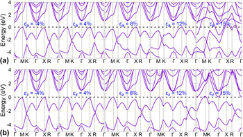
The band structures under the uniaxial strains (ε ≤ 15%) along armchair and zigzag directions are plotted in Fig. 5. From Fig. 5(a), one can see that monolayer C3N turns out to be metallic when uniaxial tensile strain along armchair direction is larger than 12%, because the conduction band at the Γ point shifts down to the Fermi level and at the same time the valence bands around the R point rises up to the Fermi level. Interestingly, the Dirac point (located at about −2.25 eV) will move away from the K point to the M point. On the other hand, for the uniaxial strain along zigzag direction, one can observe from Fig. 5(b) that monolayer C3N still transforms into a metallic phase if the amount of tensile strain is large enough (ε ≥ 15%), but it differs from the case of armchair uniaxial strain that the valence band at the M point will rise up to the Fermi level. Another difference from the uniaxial strain along armchair direction is that the Dirac point moves away from the R point to the Γ point. In fact, the R and the K points in uniaxial strained lattices originate from two inequivalent sublattices (usually called the K and K′ points) in unstrained lattice, both of which possess the linearly massless Dirac cones. When uniaxial strains (along either armchair or zigzag directions) are applied, the Dirac point only emerges along one path (either the K–M or the R–Γ lines) due to the reduction of crystal symmetry. This can also be seen from the compression strain along armchair direction [leftmost panel in Fig. 5(a)] and its effect is similar to the tensile strain along zigzag direction, and vice versa [leftmost panel in Fig. 5(b)].
(a, b) The band structures of monolayer C3N under uniaxial strains along armchair and zigzag directions, respectively. The Fermi level is set to valence band maximum.

Next, we turn our attention to the elastic responses of monolayer C3N, including linear and nonlinear parts. At very small deformations, the linear elastic response is determinative, given by the generalized Hooke’s law σ ij = c ijkl ε kl , where c is the second-order stiffness tensor, σ and ε are the Cauchy stress and strain tensors respectively. By considering the plane-stress condition, the Hooke’s law in 2D isotropic system takes the form,
 $$\left[ \matrix{ {\sigma _{xx}} \hfill \cr {\sigma _{yy}} \hfill \cr {\sigma _{xy}} \hfill \cr} \right] = \left[ {\matrix{ {{C_{11}}} {{C_{12}}} 0 \cr {{C_{12}}} {{C_{11}}} 0 \cr 0 0 {{{{C_{11}} - {C_{12}}} \over 2}} \cr} } \right] \left[ \matrix{ {\varepsilon _{xx}} \hfill \cr {\varepsilon _{yy}} \hfill \cr 2{\varepsilon _{xy}} \hfill \cr} \right]\quad ,$$
and the in-plane stiffness constants are defined as C ij = (1/S 0)(∂2 E s/∂ε i ∂ε j ), where S 0 is the equilibrium area and the strain energy E s is defined as the energy difference between the strained and unstrained systems. The other mechanical quantities, such as the Poisson’s ratio, Young’s and shear moduli can be obtained accordingly, Reference Wei and Peng42
 $$\nu = {{{C_{12}}} \over {{C_{11}}}},\quad E = {{C_{11}^2 - C_{12}^2} \over {{C_{11}}}},\quad G = {{{C_{11}} - {C_{12}}} \over 2}\quad .$$
Note that the Poisson’ ratio and Young’s modulus calculated from above equations should be the same as the values of ν(ε → 0) [Fig. 3(b)] and the slope of the stress–strain curve at small strain [Fig. 3(a)] respectively. We also calculate the bulk modulus of monolayer C3N using the formula K = S 0∂σ/∂S, where σ is the hydrostatic (biaxial) stress, S 0 and S are the equilibrium and strained areas. Thus, above four elastic moduli are not fully independent, and their relations are written as, Reference Jasiuk, Chen and Thorpe43
 $$K = {E \over {2(1 - \nu )}},\quad G = {E \over {2(1 + \nu )}}\quad .$$
Hence, the linear elastic properties of an isotropic system can be uniquely determined by any two moduli among them.
The nonlinear elasticity usually becomes important at large strain, such as in graphene, Reference Lee, Wei, Kysar and Hone13,Reference Cadelano, Palla, Giordano and Colombo39 which can be captured by a phenomenological nonlinear scalar relation,
 $$\sigma = E{\varepsilon _{\rm{L}}} + D\varepsilon _{\rm{L}}^2\quad ,$$
where εL is the Lagrangian strain, E and D are the linear (second-order) and nonlinear (third-order) elastic modulus respectively. By fitting the stress–strain curves in Fig. 3(a), the nonlinear elastic moduli along armchair, zigzag, and biaxial directions, i.e., D a, D z, and D b, can be derived separately. The values of D are typically negative in 2D materials, such that the weakening of stiffness turns up at large tensile strains. Reference Lee, Wei, Kysar and Hone13,Reference Cadelano, Palla, Giordano and Colombo39
The calculated linear and nonlinear elastic moduli of monolayer C3N and graphene are collected in Table I. Our calculated various elastic moduli of graphene are in good agreement with previous theoretical and experimental reports, which confirms the validity of computational methods used here. By comparing the results of graphene and monolayer C3N, it is interestingly found that monolayer C3N is a stiffer 2D material than graphene due to the larger linear elastic moduli (e.g., the Young’s modulus). Furthermore, the nonlinear effect of elasticity is more remarkable in monolayer C3N. The largest nonlinear elastic modulus appears in biaxial strain and slight anisotropy presents under uniaxial strains along armchair and zigzag directions, which can also be easily observed in Fig. 3(a).
The linear and nonlinear elastic moduli of monolayer C3N and graphene. Available theoretical and experimental data of graphene are listed for comparisons. The elastic moduli are in the units of N/m except for the dimensionless Poisson’s ratio.

a Ref. Reference Peng, Han, Lian, Wen, Liu, Chen, Koratkar and De35 (Theory).
b Ref. Reference Kalosakas, Lathiotakis, Galiotis and Papagelis38 (Theory).
c Ref. Reference Cadelano, Palla, Giordano and Colombo39 (Theory).
d Ref. Reference Zhou and Huang40 (Theory).
e Ref. Reference Kudin, Scuseria and Yakobson36 (Theory).
f Ref. Reference Zakharchenko, Katsnelson and Fasolino41 (Theory).
g Ref. Reference Lee, Wei, Kysar and Hone13 (Experiment).
Since monolayer C3N is a narrow band-gap semiconductor, it is urgent to know its optical manifestations. Here, we compute the optical properties of monolayer C3N by using the Wannier functions,
Reference Mostofi, Yates, Lee, Souza, Vanderbilt and Marzari31
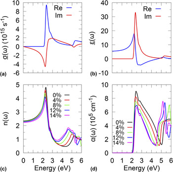
which are constructed from the Bloch functions converged by the HSE06 potential. The first-principles calculated and the Wannier-interpolated band structures are plotted together in Fig. 2(b), which shows the enough accuracy for post-processing optical calculations. The real (absorptive) and imaginary (dispersive) parts of optical conductivity of monolayer C3N are presented in Fig. 6(a), from which one can see that the peak absorption happens at the photon energy of ∼2.3 eV where the dispersive curve changes its sign because of the Kramers–Kronig relation. Both real and imaginary parts of optical conductivity reduce gradually to zero at the high energy region (>6 eV). In Fig. 6(b), we plot the dielectric function of monolayer C3N calculated by the formula
 $\underline{\varepsilon} (\omega ) = 1 + 4\pi {\rm{i}}\underline{\sigma} (\omega ){\rm{/}}\omega$
. The imaginary part of dielectric function
 $\left( {{\underline{\varepsilon} _2}} \right)$
has a peak located at ∼2.3 eV, which exactly corresponds to the real part of optical conductivity
 $\left( {{\underline{\sigma} _{\rm{1}}}} \right)$
. Similar to the
 $\underline{\sigma}$
, both real and imaginary parts of
 $\underline{\varepsilon}$
reduce gradually to zero as the increasing of photon energy.
(a, b) The optical conductivity and dielectric function of monolayer C3N. (c, d) The absorption coefficient and refractive index of monolayer C3N as a function of biaxial strains.

From the dielectric function, we can obtain the refractive index
 $n = {{{{\left[ {{{\left( \underline{{\varepsilon}} _{\rm{1}}^{\rm{2}} + \underline{\varepsilon} _{\rm{2}}^{\rm{2}}} \right)}^{{\rm{1/2}}}} + \underline{{\varepsilon}} _{\rm{1}}}} \right]}^{{\rm{1/2}}}}} \mathord{\left/ {\vphantom {{{{\left[ {{{\left( {\varepsilon _{\rm{1}}^{\rm{2}} + \varepsilon _{\rm{2}}^{\rm{2}}} \right)}^{{\rm{1/2}}}} + {\varepsilon _{\rm{1}}}} \right]}^{{\rm{1/2}}}}} {{{\rm{2}}^{{\rm{1/2}}}}}}} \right. \kern-\nulldelimiterspace} {{{\rm{2}}^{{\rm{1/2}}}}}}$
and the absorption coefficient α(ω) = ωε2/(cn), where c is the speed of light. Considering the superior flexibility of 2D materials, the applied strains can sustain to a relatively large scale and subsequently the electronic structure and optical response can be engineered effectively. Here, we present the strain effect on the refractive index and absorption coefficient of monolayer C3N, shown in Figs. 6(c) and 6(d) respectively. Inherited from the feature of the dielectric function, the refractive index has a spike peak around 2.3 eV and it slightly decreases as the increasing of strain. At high photon energy, the refractive index of monolayer C3N eventually tends to the unit one. For the absorption spectrum, the major peak appears in a broad energy range of 2.0–4.5 eV, which indicates the pronounced absorption of visible light in monolayer C3N. Interestingly, this major peak shrinks obviously at large strain, which may be ascribed to the reduction of band gap as the increasing of strain [see Fig. 3(d)]. Furthermore, the secondary absorption peak located in the ultraviolet region (>4.5 eV) exhibits significant enhancement and red shift as the increasing of strain. This demonstrates that strain can effectively mediate the ratio of absorptions between visible and ultraviolet regions in monolayer C3N.
IV. SUMMARY
In summary, based on the first-principles calculations, we investigated the electronic, mechanical, and optical properties of monolayer C3N, a newly synthesized 2D nitrogen-graphene crystal. Monolayer C3N is an indirect band-gap semiconductor rather than the semimetallic graphene due to the electron doping from two substituted N atoms in graphene lattice. It is slightly weaker than graphene due to the smaller ideal strength but is stiffer than graphene due to the larger linear elastic moduli. Monolayer C3N also presents prominent nonlinear effect of elasticity. Finally, large optical absorption can be achieved in a wide energy range including the visible and ultraviolet lights and strain can effectively mediate the ratio of them. Our results suggest monolayer C3N could be a potential 2D material for future electronic and optoelectronic device applications.
ACKNOWLEDGMENTS
This work was supported by the NSF of China (Grant Nos. 11374033 and 11574029), the MOST Project of China (Grant Nos. 2014CB920903 and 2016YFA0300600), and the Specialized Research Fund for the Doctoral Program of Higher Education of China (Grant No. 20131101120052).