

1 Introduction
Helicon plasma sources produce low temperature, high-density and low-pressure plasmas (Chen Reference Chen, d’Agostino, Favia, Ikegami, Kawai, Sato and Arefi-Khonsari2006). Nowadays, accessible and economical helicon plasma sources are attractive assets which are used as the particle source for accelerators, inertial electrostatic confinement fusion devices and plasma jets as well as for the electron source for pre-ionization in magnetic confinement devices (Hwang, Hong & Eom Reference Hwang, Hong and Eom1998; Chen Reference Chen2008).
Chen has studied the physical mechanism of antenna and the propagation of electromagnetic and electrostatic fields in helicon discharges (Chen Reference Chen1996). The theory of helicon plasma discharge, and the calculation of the antenna resistivity and plasma resistance are studied by Park and his colleagues (Park, Choi & Yoon Reference Park, Choi and Yoon1997). A comparative study of the several radio frequency antennae, which are common in helicon plasma sources, is theoretically performed by Melazzi (Melazzi & Lancellotti Reference Melazzi and Lancellotti2015). Caneses and his colleagues have investigated wave propagation and collisional absorption of the helicon waves in a high-pressure hydrogen helicon plasma source (Caneses & Blackwell Reference Caneses and Blackwell2016).
Several studies have been performed to improve the ionization efficiency of helicon plasma sources. Researchers have tried to design an optimal plasma source. Miljak and Chen have found that by using phased bifilar antennae, helicon waves are excited by applying fields which rotate either in space or in time, or both simultaneously. Since helicon waveforms are helices which rotate in both space and time, one can obtain a higher plasma density by improving the antenna coupling with the plasma by using either antennae that are themselves helices or those with fields that rotate in time (Miljak & Chen Reference Miljak and Chen1998). In another work, reported in 2005, an optimal configuration for the helicon antenna was proposed by Guittienne and Chevalier Towards (Guittienne, Chevalier & Hollenstein Reference Guittienne, Chevalier and Hollenstein2005). They proposed a birdcage form antenna for helicon wave excitation.
Nowadays, use of computational codes and standard software are interesting for the investigation and study of different aspects of plasma production in helicon plasma sources. In this regard, a direct numerical simulation model of a helicon plasma discharge with three-dimensional two-fluid equations has been employed by Yang and his colleagues to study the characteristics of the temporal evolution of the electron density and temperature. They used the finite element solver in COMSOL Multiphysics to solve all of the partial differential equations (Xiong et al. Reference Xiong, Cheng, Dawei, Moge and Xiaokang2017).
Using computational codes and the COMSOL Multiphysics software, Caneses, et al. have investigated antenna radiation patterns in the vicinity of a helicon antenna in a hydrogen plasma in the MAGPIE and the Proto MPEX linear plasma devices (Caneses, Blackwell & Piotrowicz Reference Caneses, Blackwell and Piotrowicz2017). One of the important aspects, which can affect the efficiency of helicon plasma sources, is the symmetry or asymmetry of the effective parameters. Symmetry in the configuration, patterns and distribution of the helicon plasma discharge components can increase the coupling of the helicon wave with the plasma. Therefore, studying the symmetry or asymmetry of the helicon plasma discharge parameters can help us to design and improve the parameters of a helicon plasma source.
In this way, Black and Chen have found that the Faraday shield can block the electrostatic field in the helicon discharge (Blackwell & Chen Reference Blackwell and Chen1997). They have seen that the plasma density profile has a symmetrical pattern in this situation. They could observe the effect of capacitive coupling, which is usually neglected in theory, by inserting a Faraday shield between the antenna and the glass chamber. It is shown that even in high-density regimes where the plasma has been referred to as ‘wave coupled’ (Ellingboe & Boswell Reference Ellingboe and Boswell1996), capacitive coupling can have a significant effect on the plasma properties. Another important parameter is the antenna geometry. We found that the influence of the current ports of the antenna was not taken into account in the previous works. Our simulation results show that the antenna current ports (in Nagoya III), can affect the symmetry of the electromagnetic field patterns in the helicon plasma discharge system. In this work, a new configuration for the antenna is proposed which protects the symmetry of the wave field patterns. Our simulation shows that if a Nagoya antenna (type III) with two sets of symmetrical ports is used in the helicon plasma source, the helicon wave field components represent symmetrical patterns. The influence of the electromagnetic wave pattern symmetry on the plasma density as well as power absorption in the helicon plasma source with a common Nagoya antenna is analysed by using the standard COMSOL Multiphysics 5.3 software.
The simulation results show that density of the plasma, which is produced by using our proposed antenna, increases by a factor of two in comparison to the common antenna. This result indicates that the symmetry of the field patterns can affect the plasma density and power absorption and plays a vital role in increasing of wave–particle coupling. This fact has not been reported in the previous literature. It should be noted that all parameters and interactions with cross-sections for energies of 0.001 eV to 1 MeV are included in the simulation.
Finally, the aim of this work can be represented in two items: first, proposing a new configuration for the antenna which increases the power absorption and the plasma density. Second, thanks to this new antenna, we can study and compare our simulation results with the experimental outcomes of the operational helicon plasma source devices.
The manuscript is organized as follows: the theory of the work is presented in § 2, § 3 describes the simulation results for a the common Nagoya antenna as well as our proposed antenna and deals with the plasma production by using these two antenna types. At the end, the paper is concluded in the § 4.
2 Theory
Helicon waves in the simplest form are derived from the three linearized Maxwell equations, momentum equation and Ohm’s law. Using a cylindrical coordinates, the Maxwell equations lead to the Bessel equations for the magnetic field components of the helicon wave. Subsequently, Lenz’s law leads to the electric field components of the helicon wave. This equation in cylindrical coordinates forms the Bessel equation for the magnetic field components of the helicon wave (Chen Reference Chen1991, Reference Chen2012; Ziemba et al. Reference Ziemba, Euripides, Slough, Winglee, Giersch, Carscadden, Schnackenberg and Isley2006).
The magnetic field components of the helicon wave are obtained as:
 $$\begin{eqnarray}\displaystyle & \displaystyle B_{r}=A[(\unicode[STIX]{x1D6FC}+k)\text{J}_{m-1}(Ta)+(\unicode[STIX]{x1D6FC}-k)\text{J}_{m+1}(Ta)], & \displaystyle\end{eqnarray}$$
 $$\begin{eqnarray}\displaystyle & \displaystyle B_{\unicode[STIX]{x1D703}}=A[(\unicode[STIX]{x1D6FC}+k)\text{J}_{m-1}(Ta)-(\unicode[STIX]{x1D6FC}-k)\text{J}_{m+1}(Ta)], & \displaystyle\end{eqnarray}$$
 $$\begin{eqnarray}\displaystyle & \displaystyle B_{z}=-2\text{i}TA\text{J}_{m}(Ta), & \displaystyle\end{eqnarray}$$
where
 $a$
is equal to the chamber radius
 $r_{p},\text{J}_{m-1},\text{J}_{m+1}$
and
 $\text{J}_{m}$
are the Bessel functions of order
 $m-1,m+1,m$
respectively, and in the above relations,
 $A$
is a constant parameter which is equal to
 $\sqrt{2}/2$
. In the above equations
 $\unicode[STIX]{x1D6FC}=\unicode[STIX]{x1D714}\unicode[STIX]{x1D714}_{p}^{2}/k_{\Vert }\unicode[STIX]{x1D714}_{c}c^{2}$
,
 $\unicode[STIX]{x1D714}_{c}=eB_{0}/me$
,
 $\unicode[STIX]{x1D714}_{p}^{2}=4\unicode[STIX]{x03C0}n_{0}e^{2}/m$
,
 $c$
is speed of light,
 $k$
is the helicon wave vector,
 $\unicode[STIX]{x1D714}$
is the frequency of the helicon wave,
 $k_{\Vert }$
is the axial component of the wave vector and
 $T$
is the transverse component of the wave vector. Using the Lenz’s law and components of the magnetic field, the electric field components of the helicon wave can be obtained as;
 $$\begin{eqnarray}\displaystyle & \displaystyle E_{r}=\text{i}(\unicode[STIX]{x1D714}/k)A[(\unicode[STIX]{x1D6FC}+k)\text{J}_{m-1}-(\unicode[STIX]{x1D6FC}-k)\text{J}_{m+1}] & \displaystyle\end{eqnarray}$$
 $$\begin{eqnarray}\displaystyle & \displaystyle E_{\unicode[STIX]{x1D703}}=-(\unicode[STIX]{x1D714}/k)A[(\unicode[STIX]{x1D6FC}+k)\text{J}_{m-1}+(\unicode[STIX]{x1D6FC}-k)\text{J}_{m+1}] & \displaystyle\end{eqnarray}$$
 $$\begin{eqnarray}\displaystyle & \displaystyle E_{z}=0. & \displaystyle\end{eqnarray}$$
It is clear that the helicon wave has TE (Transverse Electric) mode characteristics. The patterns of the electric and magnetic fields of the helicon wave are plotted for
 $m=+1$
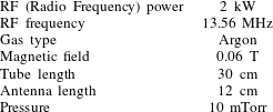
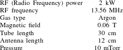
mode in figure 1. This figure shows the field components of the helicon device with the parameters as listed in table 1. A symmetrical pattern for the magnetic and electric fields appears in figure 1.
Pattern of magnetic (solid) and electric (dashed) field lines for
 $m=+1$
of helicon waves in a plane perpendicular to the DC magnetic field.

These results are derived based on the theoretical model, where the current ports of the antenna and their effects are ignored in this analysis. The influence of the current ports cannot be investigated using analytical methods and is analysed by using the COMSOL Multiphysics 5.3 software in the next section.
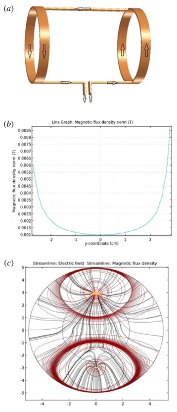
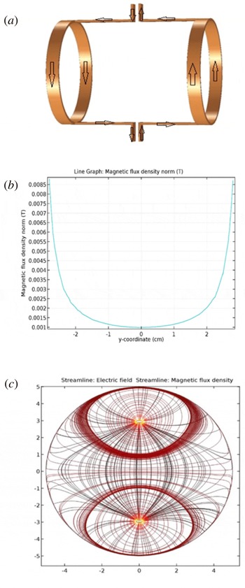
(a) The common Nagoya antenna, (b) the magnitude of the magnetic field of the helicon wave, (c) the symmetry of the electric and magnetic fields of the helicon wave pattern.
3 Design and simulation
The magnetic and electric field patterns of the electromagnetic wave produced by the two types of antennae, the common Nagoya antenna with one set of current ports and our proposed antenna with two sets of symmetrical ports, are simulated. The simulation experiments are conducted under the same theoretical model and parameters of the system, which are listed in table 1.
Parameters of the helicon plasma source.
The quintessence of our original idea is a new configuration for the antenna of helicon plasma sources designed to modify the performance of the antenna and to increase the plasma density. Because of the current ports effects in the common Nagoya antenna, the symmetries of the magnetic and electric field patterns in the helicon sources are broken. In figure 2(a), a schematic view of the common Nagoya antenna with one current port set is represented. The magnitude of the magnetic field of the helicon wave with respect to the
 $y$
axis, in the (
 $x$
–
 $y$
) plane which passes from the central point of the antenna axis is plotted in figure 2(b). Additionally, the helicon wave pattern of this common Nagoya antenna is simulated for mode
 $m=+1$
in figure 2(c). Figure 2(b,c) indicates that the symmetries of the electric and magnetic fields of the helicon wave pattern have disappeared.
On the other hand, in figure 3(a) a schema of our modified antenna with two sets of current ports is represented. The magnitudes of the magnetic fields of the helicon wave and the electric and magnetic field pattern
 $s$
of the helicon wave pattern for our proposed antenna for mode
 $m=+1$
, for the same condition as figure 2, are plotted in figure 3(b,c) respectively.
(a) The proposed antenna (two set of current ports), (b) the magnitude of the magnetic field of the helicon wave (proposed antenna), (c) the symmetry of the electric and magnetic fields of the helicon wave pattern (proposed antenna).
It is worthwhile to mention that in all of the above plots the coordinate system is chosen such that the
 $z$
axis is coincident with the axis of the antenna and the chamber. The simulation results show that the helicon wave pattern which is generated by the new modified antenna is symmetric, as expected. In other words, the use of an extra two current ports, located just opposite the first current ports, can eliminate the distortion effects of the first current ports in the helicon wave pattern.
Figures 4 and 5 represent the electromagnetic field pattern of the helicon wave in two different cross-sections for the common antenna with one port set (4
a,b) and our modified antenna (panels 5
a,b). Figures 4(a) and 5(a) are plotted in a plane which crosses the central point of the antenna axis
 $z=L/2$
(
 $L$
is the antenna length). The panels 2(a,b) are plotted in a plane which passes the antenna axis at the end point
 $z=L$
. The symmetry of the electromagnetic field patterns of our proposed antenna and the asymmetry of the electromagnetic field patterns of the common antenna (with one set of current ports) are evident in all of the different cross-sections of figures 4 and 5.
(a) Electromagnetic field patterns of common antenna (
 $z=L/2$
(
 $L$
is antenna length)), (b) electromagnetic field patterns of common antenna (
 $z=L$
(
 $L$
is antenna length)).

(a) The electromagnetic field patterns of our proposed antenna (
 $z=L/2$
(
 $L$
is antenna length)), (b) the electromagnetic field patterns of our proposed antenna (
 $z=L$
(
 $L$
is antenna length)).

The symmetry of the electric and magnetic fields of the helicon wave causes an increase of the absorption power and the plasma density. The power absorption density, plasma density and saturation time of the system for the common Nagoya antenna and our modified antenna are plotted in figures 6(a–c) and (7 a–c) respectively.
(a) Power absorption density (common Nagoya antenna), (b) plasma density (common Nagoya antenna), (c) saturation time of the system for common Nagoya antenna.

(a) Power absorption density (proposed antenna), (b) plasma density (proposed antenna), (c) saturation time of the system for our modified antenna (proposed antenna).

According to figure 6(a,b), the power absorption density and plasma density of our modified antenna with two sets of current ports is twice that of the common Nagoya antenna with one set of current ports.
In the presence of an axial magnetic field, charged particle trajectories are symmetrical helices. On the other hand, for strong coupling between the particles and wave, helicon waveforms must be helices (Miljak & Chen Reference Miljak and Chen1998). This wave is induced by a Nagoya antenna in our work. The magnetic and electric field component patterns of the helicon wave (in the absence of the current port effect) display dipole symmetry. The electric field which is produced by the antenna at fixed
 $z$
can be made to rotate in time. As indicated in figures 2, 4 and 6, the presence of one set of current ports on one side of the antenna can destroy the dipole symmetry of wave field patterns. Asymmetry of the wave field components causes acceleration or deceleration of a charged particle in the wrong direction and time. Therefore, particle trajectories deviate from the form of symmetrical helices, the same as particles rotating off-phase in respect to the helicon wave. As a result, coupling of the helicon wave and charged particles can be weakened and wave–particle energy exchange will decrease. On the other hand, our simulation results in figures 3, 5 and 7 indicate that asymmetry of the helicon wave field components is significantly improved by using two symmetrical sets of current ports. Therefore, it is expected that particles are accelerated/decelerated in the proper direction, time and space by the helicon wave field components. As a result, the helicon wave and charged particles are coupled strongly and wave–particle energy exchange will be increased.
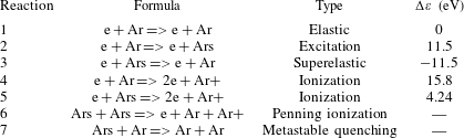
The model which is employed by the COMSOL software studies argon plasma chemistry with the following set of collisions types; elastic, excitation, direct ionization and stepwise ionization. Penning ionization and metastable quenching are also involved in the model.Footnote 1 These collisions and reactions are listed in table 2.
Table of collisions and reactions modelled (see footnote 1).

As mentioned in the help of the COMSOL software (see footnote 1), stepwise ionization (reaction 5) can play a significant role in sustaining low-pressure argon discharges. Excited argon atoms are consumed via superelastic collisions with electrons, quenching with neutral argon atoms, ionization or Penning ionization where two metastable argon atoms react to form a neutral argon atom, an argon ion and an electron. Reaction number 7 is responsible for heating of the gas. The 11.5 eV of energy which is spent in creating the electronically excited argon atom is returned to the gas as thermal energy when the excited metastable quenches. In addition to volumetric reactions, the following surface reactions are implemented as shown in table 3:
Table of surface reactions (see footnote 1).

When a metastable argon atom makes contact with the wall, it reverts to a ground state argon atom with some probability (the sticking coefficient) (see footnote 1).
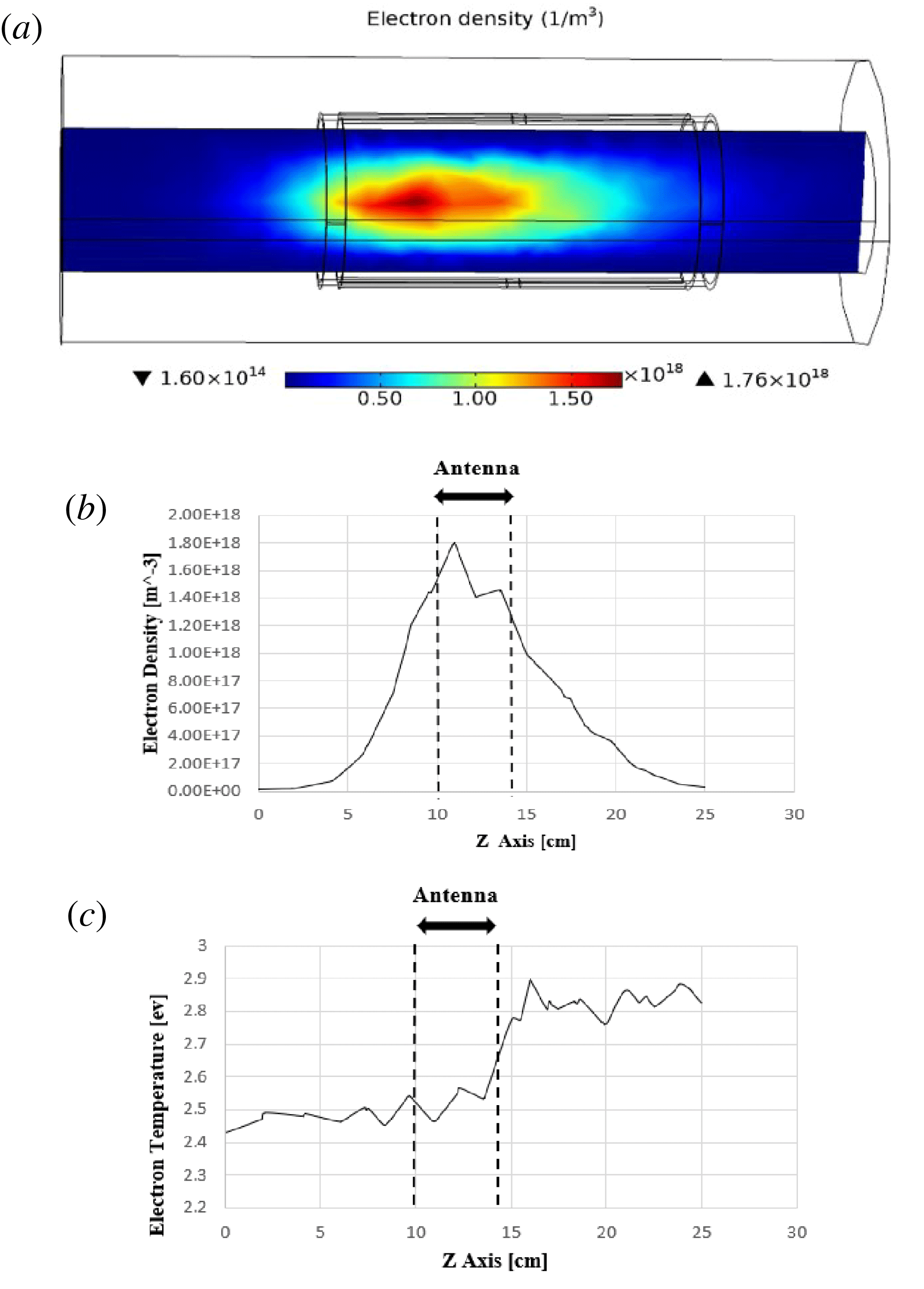
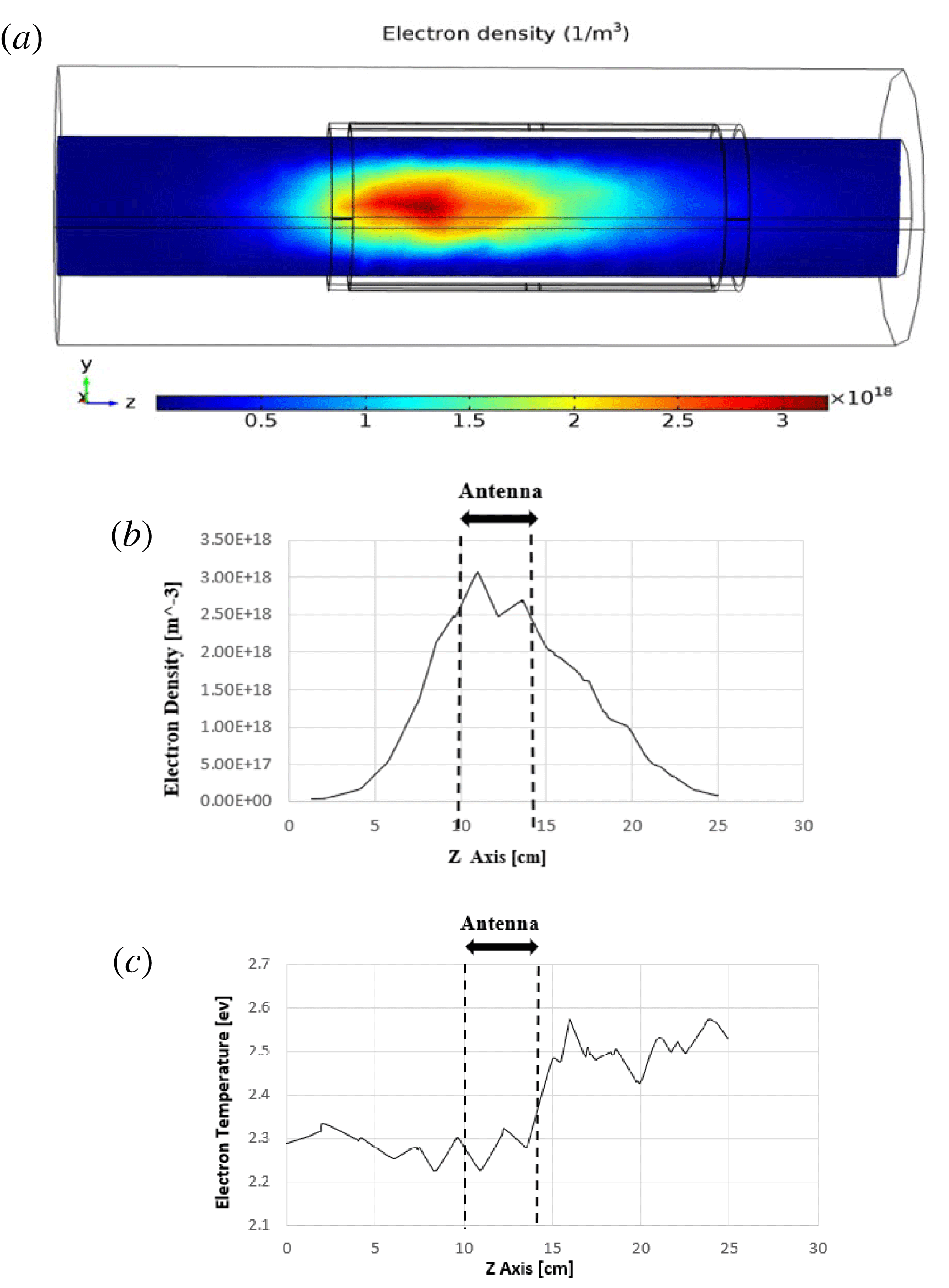
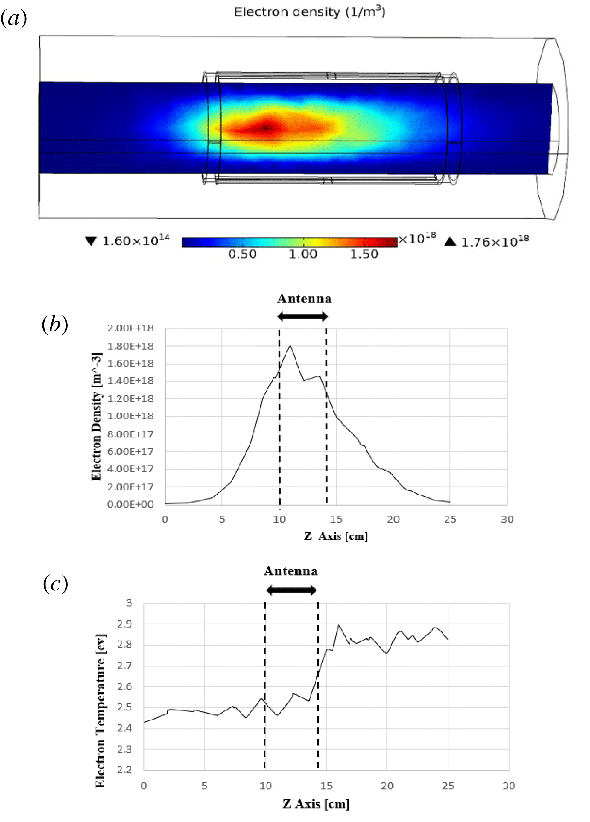
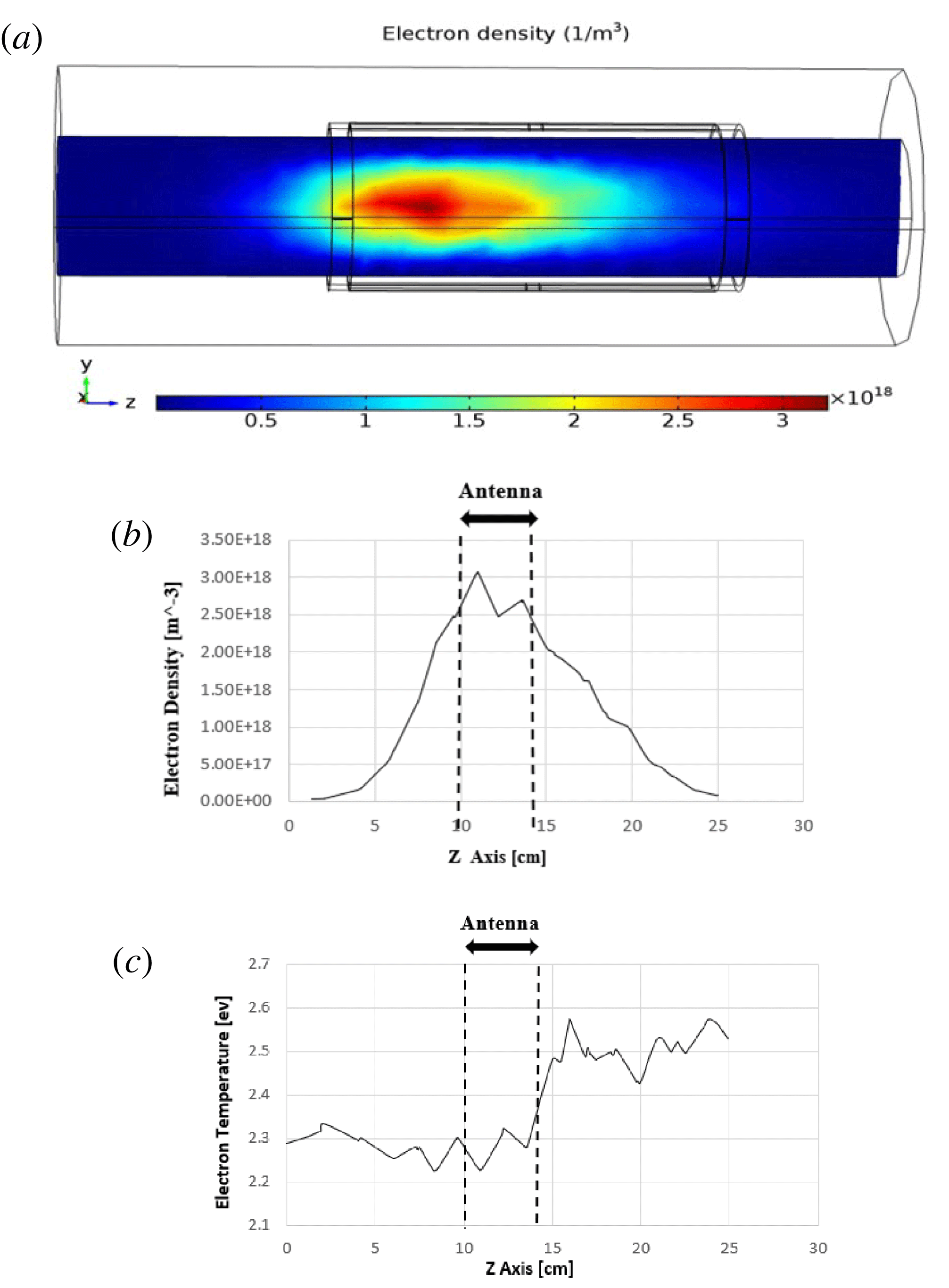
However, the helicon plasma discharge process is simulated by using a common Nagoya antenna and our proposed antenna. Variation of the electron density (plasma density), in a three-dimensional representation, is shown for the common Nagoya antenna and our proposed antenna in figures 8(a) and 9(a), respectively. The simulation results (figures 8
a and 9
a) estimate the maximum electron density of the helicon plasma discharge as approximately
 $1.7\times 10^{18}~\text{m}^{-3}$
for the common Nagoya antenna and
 $3\times 10^{18}~\text{m}^{-3}$
for our proposed antenna. Moreover, variation of the electron density is represented along the axis of symmetry (antenna axis) for two cases in figures 8(b) and 9(b). These figures represent spatial electron density distributions of two cases, along the antenna axis. Comparison of these results indicates that the form of the spatial electron density distributions is not different for the two cases and is similar to a Gaussian function. However, it is clear that the maximum electron density is increased by approximately one hundred per cent using our proposed antenna. The variation of the electron temperature along the axis of symmetry (antenna axis) is plotted, using the common Nagoya antenna figure 8(c) and our proposed antenna figure 9(c). These figures show that the electrons can reach energies of approximately 2.9 and 2.5 eV in the cases of the common Nagoya antenna and our proposed antenna, respectively. These simulation results are in good agreement with previous reports in the literature (Chen Reference Chen1996; Sudit & Chen Reference Sudit and Chen1996; Chen & Boswell Reference Chen and Boswell1997; Braginskii, Vasil’eva & Kovalev Reference Braginskii, Vasil’eva and Kovalev2001; Navarro-Cavallé et al.
Reference Navarro-Cavallé, Wijnen, Fajardo and Ahedo2018; Lee et al.
Reference Lee, Chen, Arefiev, Bengtson and Breizman2011).
The variation of the electron density in three dimensions (a), in one dimension (b) and the electron temperature (c) plotted along the antenna axis (common Nagoya antenna).
The variation of the electron density in three dimensions (a), in one dimension (b) and electron temperature (c) plotted along the antenna axis (proposed antenna).
In a number of experimental works (Light & Chen Reference Light and Chen1995; Sudit & Chen Reference Sudit and Chen1996; Miljak & Chen Reference Miljak and Chen1998) a downstream peak in the plasma density appeared along the axis of the antenna in helicon sources (in the presence of a uniform static magnetic field). This downstream density peak was explained in terms of pressure balance in Sudit & Chen (Reference Sudit and Chen1996). In this reference, the
 $z$
component of the electron equation of motion was represented as;
 $$\begin{eqnarray}\displaystyle -enE_{z}-\frac{\unicode[STIX]{x2202}}{\unicode[STIX]{x2202}z}(nKT_{e})+nmu_{z}\unicode[STIX]{x1D717}_{m}=0, & & \displaystyle\end{eqnarray}$$
where
 $n$
,
 $E_{z}$
,
 $K$
,
 $T_{e}$
,
 $u_{z}$
,
 $\unicode[STIX]{x1D717}_{m}$
and
 $m$
are plasma density,
 $z$
component of the electric field, Boltzmann constant, the electron temperature, the electron fluid velocity, the electron collision frequency for momentum transfer and the electron mass, respectively. As mentioned in this reference, in practice the collision term is negligibly small. Therefore this equation shows the downstream density peak required by pressure balance, given
 $T_{e}(z)$
and
 $E_{z}(z)$
profiles (Sudit & Chen Reference Sudit and Chen1996).
But we believe that the static magnetic field cannot be exactly uniform in practice. This downstream peak of plasma density should have been explained in terms of a pressure balance in the presence of a radial component of the static magnetic field. In fact, the axial component of the Lorentz force, which is due to the cross-product of the azimuthal component of the plasma current (
 $J_{\unicode[STIX]{x1D703}}$
) and the radial component of the static magnetic field, can displace the location of the pressure balance along the discharge tube and displace the peak of the plasma density along axis of the antenna. In our work, to reduce the simulation run time, the system is simulated in the presence of an exact uniform static magnetic field (along the axis of symmetry of the system). As a result, this term of the axial component of the Lorentz force vanishes and the peak of plasma density appears in the antenna region, which is shown in figures 8 and 9. This idea may be in agreement with the reported experimental data of the ICP system. The peak of density appeared in the antenna region in the ICP (Inductively Coupled Plasma) system (Sudit & Chen Reference Sudit and Chen1996).
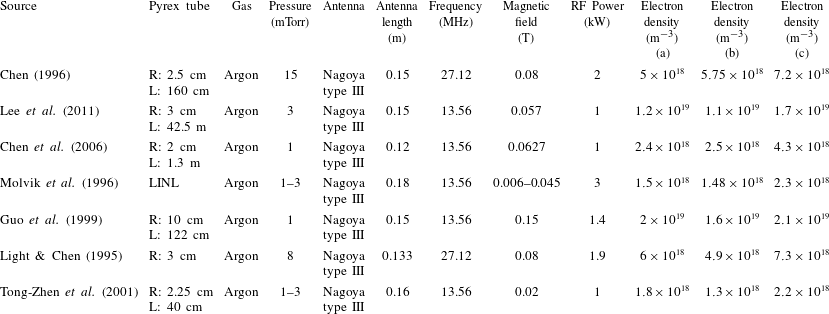
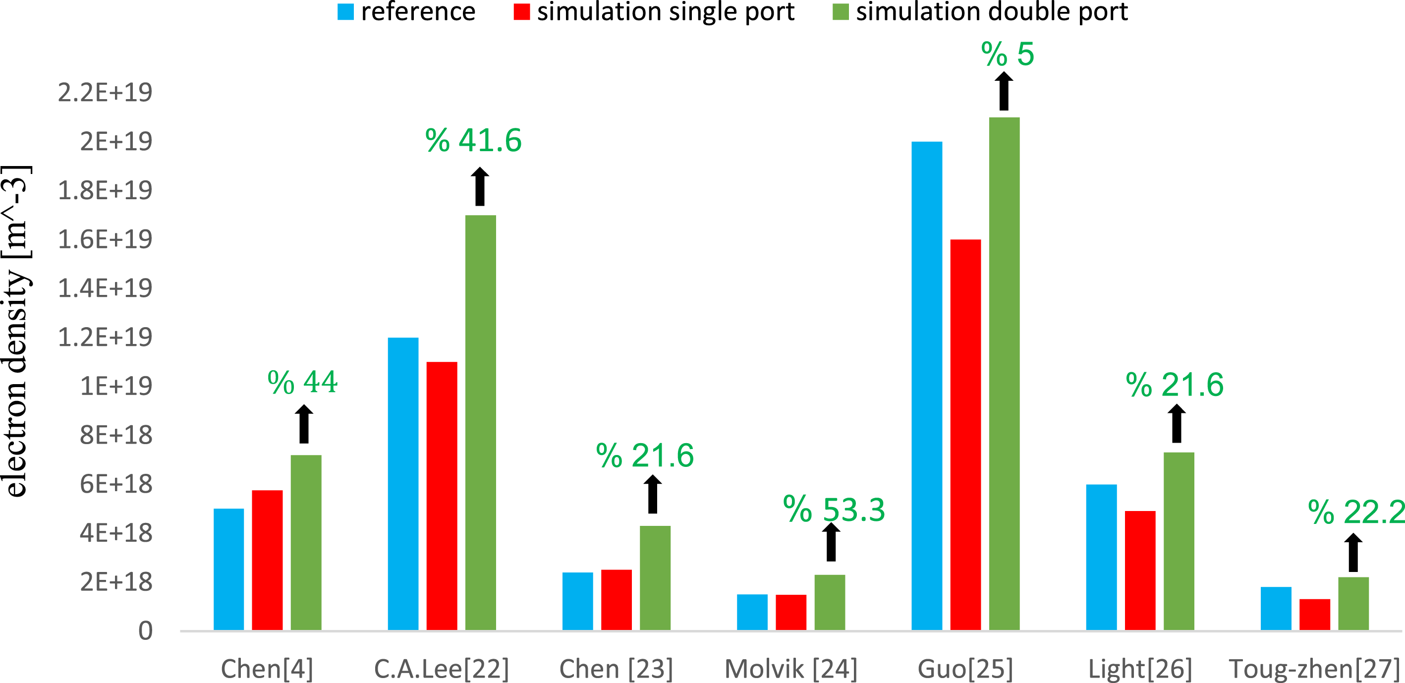
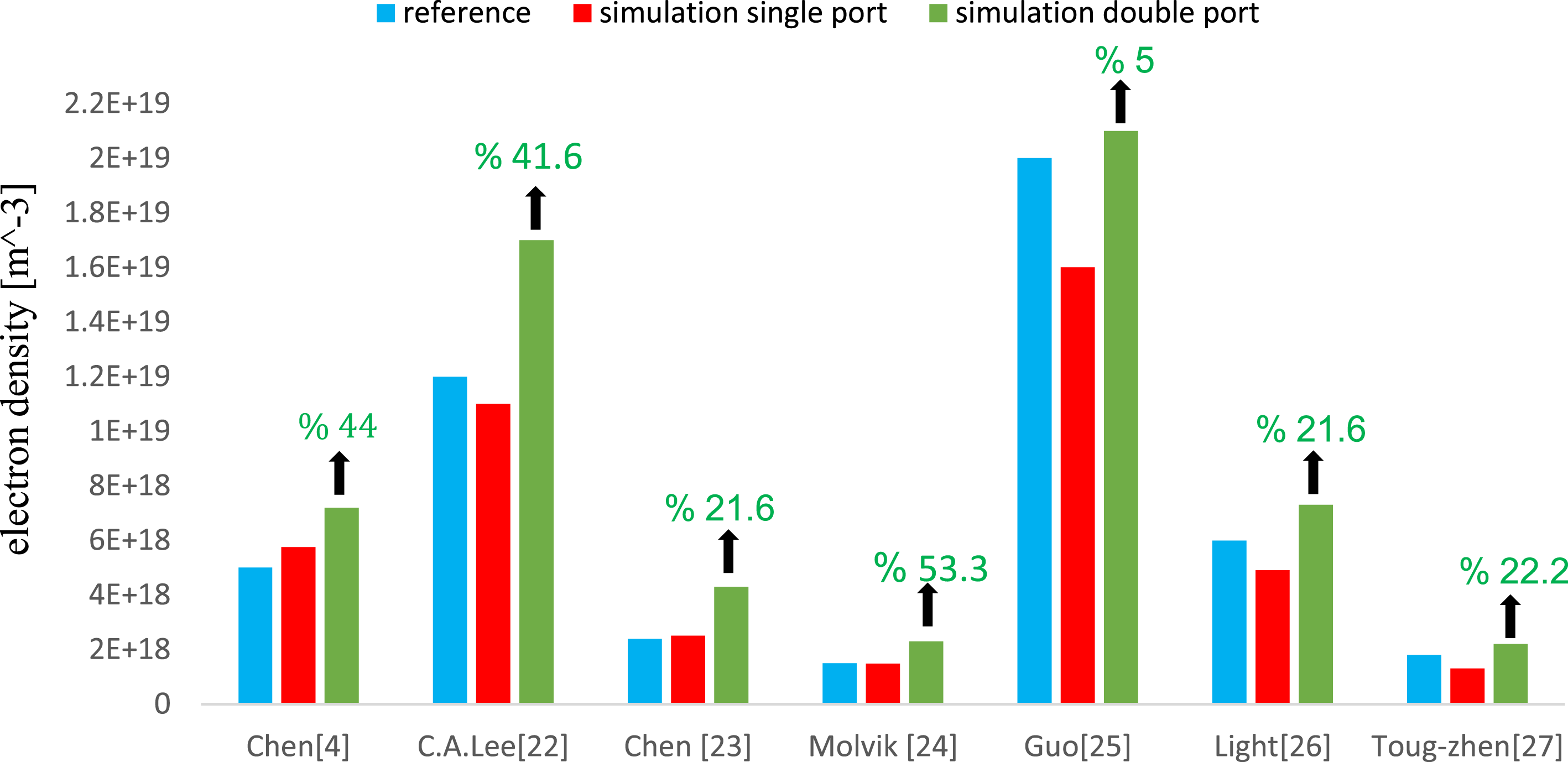
As mentioned above, the symmetry of our proposed modified antenna provides a helicon wave with a symmetric pattern of the electric and magnetic fields. In this regard, the results and data of the seven helicon plasma source devices, which are reported in references Light & Chen (Reference Light and Chen1995), Chen (Reference Chen1996), Molvik et al. (Reference Molvik, Rognlien, Byers, Cohen, Ellingboe, Hooper, McLean, Stallard and Vitello1996), Guo et al. (Reference Guo, Scharer, Mouzouris and Louis1999), Tong-Zhen et al. (Reference Tong-Zhen, Long, Di-Ming and Hou-Xian2001), Chen et al. (Reference Chen, Arefiev, Bengtson, Breizman, Lee and Raja2006), Lee et al. (Reference Lee, Chen, Arefiev, Bengtson and Breizman2011), are studied. According to the parameters of these devices, these seven devices are simulated and analysed by using the common Nagoya antenna with one set of current ports and our modified antenna with two sets of current ports individually. For validation of our simulation results, the experimental reported results of these devices are compared with our results which are obtained from simulation of these devices. This comparison shows that the plasma electron density of these devices which are reported from experiment results and the plasma density which are estimated by simulation experiments are different by approximately fifteen per cent on average. Therefore, this comparison indicates that our simulation results are reliable and a good approximation. Table 4 lists the parameters of these devices, the reported experimental data of the produced electron density and the results of our simulations. In this table, the electron plasma density which is reported in the literature from the experiment results (column a), the electron plasma density which is obtained by our simulation of the devices using the common antenna with one set of current ports (column b) and using our modified proposed antenna with two sets of current ports (column c), are represented.
The parameters and electron plasma density of the seven devices: reported experimental results (a), our simulation results using a common antenna with one set of current ports (b), our simulation results using our modified proposed antenna with two sets of current ports (c).
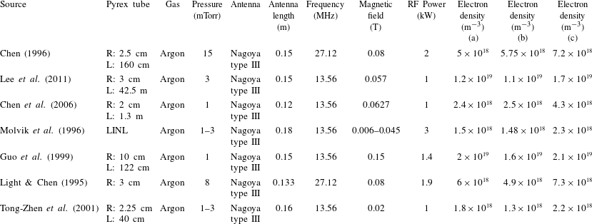
As denoted in table 4, the simulation results show that the reported experimental results confirm our simulation results for the common antenna with one set of current ports. In addition, the outcomes of the simulations indicate that using our proposed antenna, with the two sets of current ports, increases the plasma density of helicon sources in all cases, by approximately 40 % on average, in comparison to using the common antennae. The plasma density of these seven devices for the experimental results (in blue), our simulation results by using the common antenna (Nagoya) (in red) and simulation results by using our modified antenna (in green) are plotted in figure 10. The black arrows on the green columns represent the plasma density increment, as a percentage, using our proposed antenna in respect to the reported experimental data of these seven devices.
The plasma density of these seven devices for experimental results (in blue), our simulation results by using common antenna (Nagoya) (in red) and simulation results by using our modified antenna (in green).
4 Conclusion
In this paper, a helicon plasma source is simulated and analysed using a standard COMSOL Multiphysics 5.3 software. In addition, all of the parameters and interactions with cross-sections for energies of 0.001 eV to 1 MeV are included in the simulation. The simulation results show that the common Nagoya antenna with one set of current ports generates a helicon wave with an asymmetric pattern of the electric and magnetic fields. A novel modified antenna with two set of current ports is proposed to alleviate the disturbance effects of the current port on the wave pattern. It is found that the asymmetry of the helicon wave field components is significantly improved by using two symmetrical sets of current ports for the common Nagoya antenna. Therefore, it is expected that particles are accelerated/decelerated in the proper direction, time and space by the helicon wave field components. As a result, the helicon wave and charged particles are coupled strongly and wave–particle energy exchange will be increased. The analysis shows that the plasma density and the power absorption increase by approximately 40 % on average, by using our modified antenna in comparison to the reported experimental results and in comparison to the common antenna simulation results (Nagoya) with one set of current ports. This fact indicates that the symmetry of the electromagnetic wave pattern plays a vital role in increasing the power absorption rate as well as the plasma density.