Introduction
The piezotronic effect can change the electrical response of a system toward various influencing physical factors.Reference Wen, Wu, Pan, Hu, Yang and Wang1,Reference Yu, Niu, Pan and Wang2 This allows for the development of highly sensitive sensors for applications, especially in micro- and nanoelectromechanical systems (MEMS/NEMS) for robotics, photoelectric sensors, and environmental and health monitoring.Reference Zhou, Gu, Fei, Mai, Gao, Yang, Bao and Wang3–Reference Han, Chen, Pan and Wang5 Piezotronics is defined as a mechanically induced change in the potential barrier height, hence the most obvious application is stress or strain sensing. A fast (within the realm of a few microseconds) and high electrical signal resulting from the mechanical excitation is also important for piezotronic sensors. This results in short response times and high sensitivity, respectively.
Piezotronics is discussed here for a wide range of applications, including adaptive tactile sensing for electronic skins.Reference Zhou, Gu, Fei, Mai, Gao, Yang, Bao and Wang3,Reference Wu, Wen and Wang6,Reference Zhang, Zhu, Nguyen and Yang7 Piezotronic stress measurements can also be used to indirectly quantify other physical quantities such as magnetic fields.Reference Gröttrup, Kaps, Carstensen, Smazna, Mishra, Piorra, Kirchhof, Quandt and Adelung8 Due to the deformation of a magnetostrictive material, the resulting stress can be sensitively determined when coupled with a piezotronic system. For chemical and optical sensor applications, it is not necessarily the piezotronic effect itself that is the mechanism behind the working principle, rather, a large enhancement in sensing properties can be achieved when the piezotronic or piezo-phototronic effect is used.Reference Zhao, Zhou, Hua, Dong, Yu and Pan4,Reference Han, Chen, Pan and Wang5,Reference Hatch, Briscoe and Dunn9,Reference Han, Gao, Zhu, Chen, Jiang, Li, Willander, Cao and Wang10 In the case of p–n junctions and Schottky contact-based light sensors, modulation of the barrier height allows for control of charge-carrier separation, transport, and recombination (piezo-phototronic effect). This leads to tunability of the photoelectric response and hence increases the sensitivity of optical sensors. Similarly, the sensitivity of Schottky contact-based chemical sensors can be optimized by piezotronics.Reference Zhao, Zhou, Hua, Dong, Yu and Pan4,Reference Pan, Yu, Niu, Zhu and Wang11
Stress and strain sensors
Compared to commercially available technologies for stress and strain sensors, piezotronics exhibits huge advantages with respect to response time and sensitivity of stress and strain. The response time of a piezotronic nanodevice can be <5 ms.Reference Minjeong, Seongdong, Jonghwa, Doo-Seung, Youngoh and Hyunhyub12 In comparison, human tactile sensing capabilities are in the range of 30 ms.Reference Wu, Wen and Wang6 Thus, application as electronic skins for optimization of prosthetics could be highly beneficial.
A further advantage is that the piezotronic response can be used to determine both dynamic and static mechanical impact.Reference Zhang, Liao, Yan, Wang, Wang, Sun, Lin, Huang and Zhang13 The dynamic response of a system can even be obtained without an external energy supply. For quantification of the sensitivity of mechanical sensors, the gauge factor (GF) is often used to compare different technologies.Reference Liu14 The GF is defined as the relative change in resistance R normalized by the induced strain S:
 $$GF = {{\Delta R/R_0 } \over {\rm{S}}} ,$$
where R 0 is the resistance without applied mechanical stress. In recent literature, variations of this figure of merit have been discussed based on different types of applications.
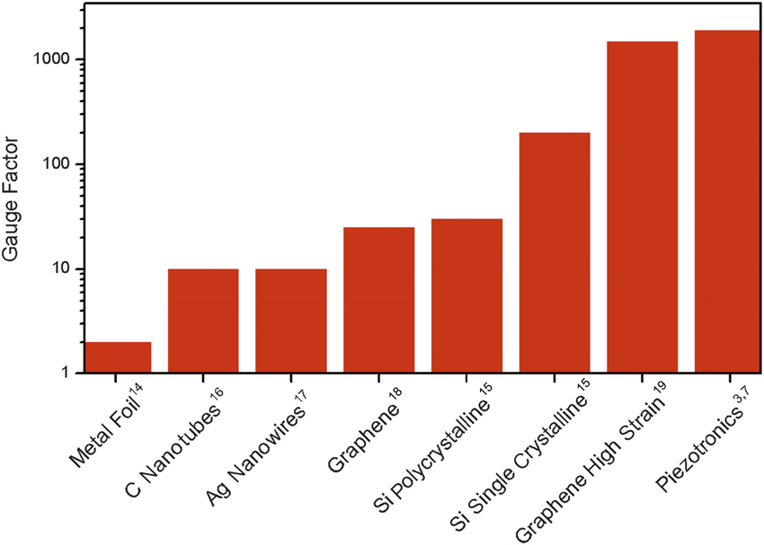
Piezotronics can be applied for both stress and strain sensors. Either a rigid array of nanowires is used to measure stress or the nanowires are deposited on flexible substrates to determine the strain response. Therefore, it might be beneficial to use the actual quantity of interest for the calculation of GF. It has been demonstrated that piezotronic sensors have a high GF (∼1000–1900) and sensitivity both in dynamic and static modes.Reference Zhou, Gu, Fei, Mai, Gao, Yang, Bao and Wang3,Reference Zhang, Zhu, Nguyen and Yang7 These values are almost an order of magnitude higher than those of the best available commercial sensors based on doped silicon (<200).Reference Liu14,Reference Barlian, Park, Mallon, Rastegar and Pruitt15
Compared to other emerging technologies, piezotronic systems are also extremely competitive (see Figure 1). In strain sensors that use composites of carbon nanotubes, graphene, and Ag nanowire, GF usually does not exceed 25.Reference Suzuki, Yataka, Okumiya, Sakakibara, Sako, Mimura and Inoue16–Reference Chen, Jiang, Lou, Chen and Shen18 For these, stretchability is the key criterion. So far, only tribotronics-based sensors (using charge generation through triboelectricity) or highly strained graphene achieve sensitivities and response times comparable to piezotronic sensors.Reference Lin, Xie, Wang, Wu, Niu, Wen and Wang19,Reference Li, Zhang, Yu, Wang, Wei, Wu, Cao, Li, Cheng, Zheng, Ruoff and Zhu20
Comparison of different materials and structures with respect to the achievable gauge factor for strain-sensing applications.

One disadvantage of piezotronics is the complex synthesis of the nanowire arrays needed for efficient sensing. Competing strategies such as the use of tribotronic systems are less challenging in this regard.Reference Lin, Xie, Wang, Wu, Niu, Wen and Wang19 However, significant progress has been made in simplifying the nanowire array synthesis and making it more efficient by facilitating cost-effective solution-based growth methods.Reference Zhang, Zhu, Nguyen and Yang7,Reference Qin, Yang and Wang21
With respect to the measurement of mechanical stress or strain, there have been endeavors to optimize the impact of the piezotronic effect. For example, graphene–ZnO interface-based structures allow for the development of highly flexible sensors with superior charge scavenging performance, leading to high current generation under mechanical stress.Reference Dukhyun, Min-Yeol, Mook, Hyeon-Jin, Hyun-Kyu, Ju-Seok, Jongbong, Seon-Mi, Jin, Hee, Sang-Woo, Jae-Young, Yoon and Min22 ZnO–ZnO interfaces with high potential barriers due to interface trap states have also been investigated.Reference Keil, Trapp, Novak, Frömling, Kleebe and Rödel23 Thus, quite different physical properties for the potential barrier have been obtained as compared to Schottky barriers and p–n junctions. For doped ZnO–ZnO interfaces, the induced piezoelectric charge can eliminate the barrier height almost entirely, resulting in an extreme stress response of the system. Two-dimensional nanomaterials that feature a high piezotronic response by employing layers as thin as three atomic layers have also been reported.Reference Wang, Liu, Gao, Pang, Yin, Feng, Zhu, Bai, Chen, Xiao, Wang, Qin and Wang24,Reference Wu, Wang, Li, Zhang, Lin, Niu, Chenet, Zhang, Hao, Heinz, Hone and Wang25
Optical and magnetic sensors
While previous categories of optoelectronic devices (especially in the field of infrared sensors) included linear sensing arrays (first generation) and 2D arrays (second generation), the impending third generation is expected to feature sensors with higher sensitivity, larger number of pixels, multicolor sensing, and fast response times.Reference Rogalski, Antoszewski and Faraone26 For a high pixel density, nanowires and quantum dots are the focus of much of the research in this area.Reference Han, Chen, Pan and Wang5,Reference Konstantatos and Sargent27 Considering multicolor sensing, the currently employed complementary metal-oxide-semiconductor-based sensors allow only weak absorption over the entire spectrum; in particular, the infrared and the ultraviolet (UV) ranges are barely resolved.
Especially for the UV range, there has been increasing demand for these sensors for chemical analysis, flame detection, and optical communication.Reference Han, Du, Yu, Pan and Wang28 Wide-bandgap materials such as ZnO are promising candidates in this regard. Sensing devices employing ohmic contacts are usually discussed. However, piezo-phototronically enhanced ZnO nanowire array sensors are showing much higher sensitivity and faster response than their counterparts with ohmic contacts. The photoresponsivity (gain of a detector) could be increased by 700% and the sensitivity by 600% (threshold level above noise). Furthermore, the reset time could be reduced to 20 ms compared to approximately 400 s for ohmic contacts.Reference Han, Du, Yu, Pan and Wang28,Reference Zhou, Gu, Hu, Mai, Yeh, Bao, Sood, Polla and Wang29 Hence, high sensitivity, high pixel density, and fast response requirements can be fulfilled. A similar enhancement of visible light detection could be achieved in CdSe nanowires.Reference Han, Chen, Pan and Wang5
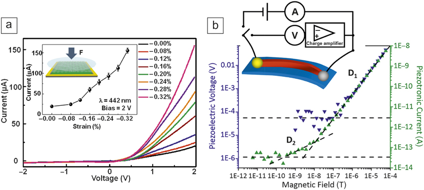
Piezo-phototronics can also improve properties of other semiconductor-based sensors by the formation of heterojunctions. For example, a sensor using a Si p–n junction with ZnO could be enhanced significantly by stress-induced changes in the junction properties (Figure 2a).Reference Wang, Yu, Wen, Liu, Pan, Wu and Wang30 The photoresponsivity could be increased by 177% and the response time shortened by 87%. Other examples include ZnO–CdS and ZnO–ZnS core–shell structure hybrids. These allow for high photoresponsivity in the visible and UV light ranges, where photoresponsivity can be increased further by an order of magnitude through piezo-phototronic modulation.Reference Zhang, Ding, Zhang, Zhang and Wang31,Reference Rai, Wang, Ding, Marmon, Bhatt, Zhang, Zhou and Wang32 For the CdS/poly(3-hexylthiophene) system even a broadband detection from UV down to near infrared could be realized.Reference Yu, Yin, Li, Zhang, Zhao, Li and Zhu33 Thus, the enhanced multicolor sensing requirement of third-generation optical sensors can also be achieved via piezo-phototronic enhancement.
(a) Current–voltage characteristics of a p-Si n-ZnO junction under different strain conditions without illumination. The inset shows the current changes with the external strains and illumination at a specific wavelength λ = 442 nm when a 2 V bias is applied to the schematically depicted p-Si/ZnO nanowire hybridized photodetector, illustrating the current gain with mechanical stress (F = applied force).Reference Wang, Yu, Wen, Liu, Pan, Wu and Wang30 (b) Sensitivity curves of a magnetoelectric sensor with standard piezoelectric readout (blue triangles, voltage mode in inset) and superior piezotronic readout (green triangles, current mode in inset). The piezotronic data feature two different slopes; D1 is the ideal Schottky contact and D2 corresponds to anonideal depletion region of the Schottky contact. The magnetoelectric sensor sketched in the inset consists of a ZnO needle (red) mounted on a magnetostrictive foil (blue) with one Schottky and one ohmic contact and an external circuit for current (A) and voltage (V) measurement.Reference Gröttrup, Kaps, Carstensen, Smazna, Mishra, Piorra, Kirchhof, Quandt and Adelung8

Another crucial advantage of piezotronics as opposed to piezoelectrics is the low noise, which allows for a low limit of detection (LOD).Reference Gröttrup, Kaps, Carstensen, Smazna, Mishra, Piorra, Kirchhof, Quandt and Adelung8 Magnetic field sensors based on magnetostrictive and piezoelectric composites are well suited to highlight this effect, as they can be read out both piezoelectrically and piezotronically. In one study, the device setup, illustrated in the inset in Figure 2b, resembles a strain sensor, but with the strain induced by a magnetostrictive material expanding in a magnetic field.Reference Gröttrup, Kaps, Carstensen, Smazna, Mishra, Piorra, Kirchhof, Quandt and Adelung8 A coupled ZnO needle is equipped with a Schottky contact on one side and an ohmic contact on the other. For piezoelectric measurements, the potential difference between the two contacts is obtained, while for piezotronic measurements, a bias voltage is added and the current flow through the needle is determined. In effect, the piezotronic readout yields a much lower LOD than a standard piezoelectric readout. The piezotronic change in charge-carrier transport acts as a signal amplifier within the material. This is preferable to piezoelectric signal amplification, which takes place outside the needle (e.g., in an external charge amplifier), thus including more noise. Furthermore, in the preferable piezotronic setup, the density of charge carriers in the depletion zone of the Schottky contact is so low that thermally activated electrons do not contribute extensively to noise. This effect can be garnered from the smaller slope in the sensitivity curve for the piezotronic readout (Figure 2b),Reference Gröttrup, Kaps, Carstensen, Smazna, Mishra, Piorra, Kirchhof, Quandt and Adelung8 as known from the two-diode model of solar cells.Reference Humada, Hojabri, Mekhilef and Hamada34 According to this model, a real Schottky contact is described by two diodes in parallel, where one diode represents an ideal Schottky contact (D1) and the other diode encapsulates the influence of a second space charge region (D2), accounting for further current paths and hence nonideality. While the signal from the space-charge region is smaller in amplitude, it is also less affected by noise, leading to a lower LOD.Reference Gröttrup, Kaps, Carstensen, Smazna, Mishra, Piorra, Kirchhof, Quandt and Adelung8
Chemical sensors
Modification of the properties of semiconducting materials caused by changes in the chemical environment has been researched and established since the 1970s.Reference Bergveld35 For example, variation in the surface potential at gate oxides in field-effect transistors (FETs) due to absorption of analytes can be used to reliably detect gases and solutes in liquids. With advancements in nanotechnology, nanostructures can be implemented for this purpose, and their high surface-to-volume ratios and short electronic charge-carrier transport paths can be facilitated.Reference Zhang and Lieber36 Even though this has led to significant enhancements of sensing systems, further optimization of sensitivity of complex nanostructured devices is complicated. The investigated ohmic contact-based devices (e.g., FET-based structures) are also quite costly.Reference Yu, Niu, Pan and Wang2 It has, however, been shown that Schottky contact-based nanowire sensors that can be piezotronically enhanced exhibit superior properties with a low-cost synthesis, compared to ohmic contact-based structures.Reference Yu, Niu, Pan and Wang2
For O2 gas-sensing, ZnO with ohmic contacts exhibited a sensitivity of 4.8% (represented as relative current change ∆I/I 0 with I 0 as the current without the analyte). Under the same conditions, a Schottky contact-based ZnO nanowire showed a sensitivity of 3235%, which translates to a 1085-fold increase in sensitivity.Reference Yu, Niu, Pan and Wang2 Applying 0.2% tensile strain further led to a significant increase in sensitivity for these structures, allowing for optimization of the system response according to the analyte concentration (similar to FET devices in which the gate voltage can be modulated externally).
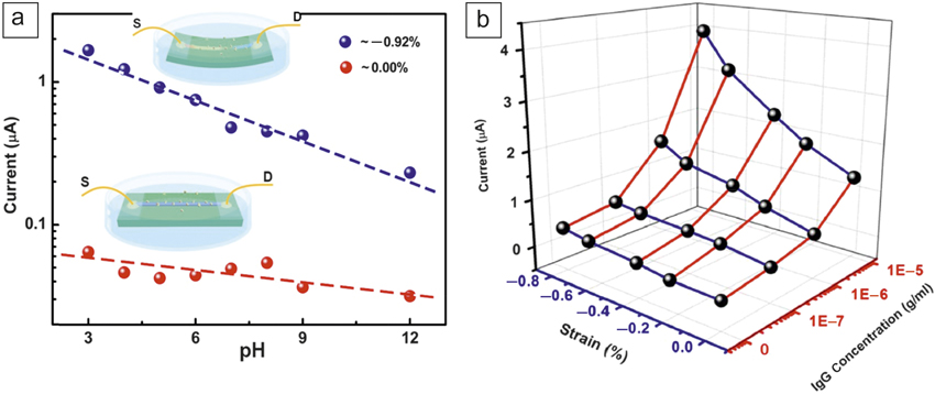
In one study, piezotronic pH sensors were fabricated by transferring a long ZnO nanowire onto a poly(ethylene terephthalate) substrate (schematically depicted in Figure 3a).Reference Pan, Yu, Niu, Zhu and Wang11 The signal level of the pH sensor is increased, and the sensitivity of the device is enhanced by the piezotronic effect. The signal level of a strain-free pH sensor of 1.2 nA (red plot in Figure 3a) is enhanced by three orders of magnitude to 1.75 μA by a compressive strain of S = –0.92% (blue plot in Figure 3a). In biomolecular sensor applications, interfacing ZnO nanowires with antibodies can lead to specific and highly sensitive sensing of proteins.Reference Yu, Niu, Pan and Wang2,Reference Yu, Pan and Wang37 Anti-Immunoglobulin G conjugates with gold particles can be attached to ZnO. Binding of the respective Immunoglobulin G (IgG) led to a change in the surface properties. Also in this case, the change from ohmic contacts to Schottky contacts resulted in enhanced sensitivity that could be further optimized via piezotronics. By applying a strain of up to –0.82%, the LOD could be enhanced so that a two orders of magnitude lower concentration of IgG could be detected compared to the system without strain (Figure 3b).
(a) The response of the sensor to pH varying from 3 to 12. Enhanced current from unstrained (red) to strained (blue) shows increased sensitivity (inset schematics depict different mechanical strain conditions for the device with S = source and D = drain).Reference Pan, Yu, Niu, Zhu and Wang11 (b) Depiction of the current response of ZnO nanowire protein sensor under different strains and Immunoglobulin G (IgG) concentrations, illustrating the increase in sensitivity with mechanical strain.Reference Yu, Pan and Wang37

These examples illustrate that the piezotronic effect can become a dominant mechanism for the development of various types of environmental sensors (e.g., radiation exposure monitoring) and will especially boost efforts toward human interfacing and medical applications such as sensors for artificial skin and blood composition control. In the future, however, more reliable methods for industrial upscaling of the devices will be important.
Acknowledgment
This work was supported by the Deutsche Forschungsgemeinschaft (DFG) under Project No. R0954/28–1 and within the CRC 1261, Project A5.

Till Frömling has been a group leader at the Technische Universität Darmstadt, Germany, since 2013. He received his BS degree in chemistry from the Philipps-Universität Marburg, Germany, and his PhD degree at the Technische Universität Wien, Austria. In 2011, he joined SB Limotive/Bosch Battery Systems working on the development of energy-storage systems. His research focuses on the defect chemistry of lead-free ferroelectrics, high-temperature capacitors, and mechanical modification of ionic and electronic conductivity of oxides. Frömling can be reached by email at froemling@ceramics.tu-darmstadt.de.

Ruomeng Yu is the Sensor Technical Lead at Amazon Lab126, which focuses on sensor systems in consumer electronics. He received his PhD degree in materials science and engineering in 2016 from the Georgia Institute of Technology. His research interests include the piezotronic effect, the piezo-phototronic effect and applications in sensors, logic circuits, and flexible electronics. He has published more than 40 papers. Yu can be reached by email at ruomengyu@gmail.com.

Mona Mintken is a doctoral candidate at Kiel University, Germany, in the Collaborative Research Center 1261 (Magnetoelectric Sensors: From Composite Materials to Biomagnetic Diagnostics). She obtained her bachelor’s and master’s degrees in materials science and engineering from Kiel University. Her research focuses on applying the piezotronic effect to magnetoelectric sensors. Mintken can be reached by email at momi@tf.uni-kiel.de.

Rainer Adelung is a professor in materials science at Kiel University, Germany. He studied physics at Kiel University, and after obtaining his doctoral degree in 2000, he changed to materials science in 2001 at Case Western Reserve University. After his Habilitation degree in 2007, he received a Heisenberg Professorship at Kiel University. Since 2010, he has been the chair for functional nanomaterials. His research focuses on porous materials and piezotronics. Since 2013, he has been a spokesperson for KiNSIS, one of the priority research areas of Kiel University. Adelung can be reached by email at ra@tf.uni-kiel.de.

Jürgen Rödel is a professor in materials science at Technische Universität Darmstadt, Germany. He obtained his diploma in materials science from the Friedrich-Alexander-Universität Erlangen-Nürnberg, Germany, and his PhD degree from the University of California, Berkeley. His research current interests include the development of lead-free piezoceramics and the concept of mechanically tuned conductivity. He has (co-)authored approximately 300 publications. He has received both the DFG research award for young scientists (Heinz-Maier-Leibnitz Prize) and for senior scientists (Gottfried Wilhelm Leibniz Prize), and he is a member of the German National Academy of Science and Engineering. Rödel can be reached by email at roedel@ceramics.tu-darmstadt.de.